

Abstract
To realize high-capacity Ge anodes for next-generation Li+-ion batteries, a multilayer anode with a C(top)/Ge(middle)/C(bottom) structure was developed, where nanostructured amorphous Ge (a-Ge) and amorphous-like carbon films with a grain size of 10–20 nm were deposited sequentially by high-pressure Ar sputtering at 500 mTorr. Compared with the a-Ge anode, the C(top)/a-Ge(middle)/C(bottom) multistacking layer anode showed improved capacity degradation for repeated lithiation/delithiation reactions and achieved a high capacity of 910 mAh g−1 with no capacity fading after 90 cycles at a C-rate of 0.1.
Export citation and abstract BibTeX RIS

Content from this work may be used under the terms of the Creative Commons Attribution 4.0 license. Any further distribution of this work must maintain attribution to the author(s) and the title of the work, journal citation and DOI.
Most commercial Li+-ion batteries (LIBs) use graphite-based carbon as an anode material; the graphite-based carbon not only exhibits a stable cycling performance but also provides a cost advantage. The theoretical Li-storage capacity of a graphite anode, however, is limited to 372 mAh g−1, and the development of higher-capacity anode materials to enable further downsizing and higher energy efficiency of LIBs is an active research area. 1,2) Si 3–6) and Ge 7–10) are promising candidates for next-generation anode materials because they have theoretical Li-storage capacities of 4200 and 1624 mAh g−1, respectively. 11,12) However, Si and Ge form alloys with Li during the charging process, resulting in a ∼400% volume expansion. 12,13) The large volume change during charge–discharge induces pulverization of the anode material and subsequent separation from the Cu current collector, which leads to rapid capacity degradation.
We have focused on Ge, which has advantages over Si for use in LIBs, including 400 times higher Li+-ion diffusivity 9) and 104 times higher electrical conductivity. 10,14) A promising approach for realizing high-capacity Ge anodes is fabricating a Ge nanostructure on a Cu current collector using nanoparticles, 7,15) where the nanomaterial can uniformly expand during Li alloying because of the large surface-to-volume ratio, reducing physical stress and suppressing material pulverization. Here, we developed a nanostructured anode by combining Ge with C materials in a low-temperature plasma process. Several authors have reported Ge–C composite anodes with various morphologies such as nanoparticles, 16,17) nanowires, 14,18) and nanoporous structures. 19,20) However, the previously reported Ge–C composite anodes were fabricated using a slurry coating process that involves mixing active Ge–C nanomaterials, polymer binders, and carbon black particles. By contrast, we used a plasma bottom-up process and fabricated a binder-free nanostructured C/Ge/C multilayer anode that exhibits both high capacity and high capacity retention.
Three types of anode films—a Ge or C monolayer film, a C(top)/Ge(middle)/C(bottom) multilayer film, and a GeC mixed film—were fabricated on a Cu anode substrate using a 13.56 MHz RF magnetron co-sputtering system [Fig. 1(a)]. 21) The Cu substrate was 15 mm in diameter and 80 μm thick and was placed in the center of the substrate holder, which was rotated at a constant speed of 3 rpm during deposition to make the film thickness and the composition uniform in the plane of the Cu substrate during sputtering at an oblique direction to the substrate. The sputtering targets were a polycrystalline Ge disk (1-inch diameter) on the left side and a graphite-structured C disk (1-inch diameter) on the right side. Discharge plasma was produced by supplying 60 W (11.8 W cm−2) RF power to both sputtering cathodes. Figures 1(b)–1(d) show photographs of the sputtering process for the Ge film, C film, and the GeC mixed film, respectively. The Ar gas pressure was as high as 500 mTorr, and the Ar gas flow rate was 100 sccm. The distances ZGe and ZC between the Ge and C targets and the center of the substrate were fixed at 40 and 30 mm, respectively. The substrate holder was not heated or cooled during deposition. The fabricated Ge monolayer film, C/Ge/C multilayer film, and GeC mixed film were assembled as anodes in LIB cells, which were sealed test cells that simulated CR2032 coin cells. A Li-metal disc with a diameter and thickness of 16 mm and 250 μm, respectively, was used as the counter electrode. A polypropylene separator with a diameter and thickness of 24 mm and 24 μm, respectively, was placed between the Ge anode and the Li cathode. The electrolyte was 1 mol l−1 LiPF6 dissolved in an ethylene carbonate (EC)–diethyl carbonate (DEC) mixture (EC:DEC = 1:1 vol%). Battery performance was analyzed at RT for all charge–discharge cycles using a battery test apparatus; the batteries were cycled at a constant current of 0.02 C-rate (32 mA g−1) for 1–2 cycles and 0.1 C-rate (160 mA g−1) for 3–90 cycles. The films were deposited onto an n-type Si wafer under the same sputtering conditions as the battery anode film. The crystal structure was evaluated by Raman spectroscopy and scanning electron microscopy (SEM).
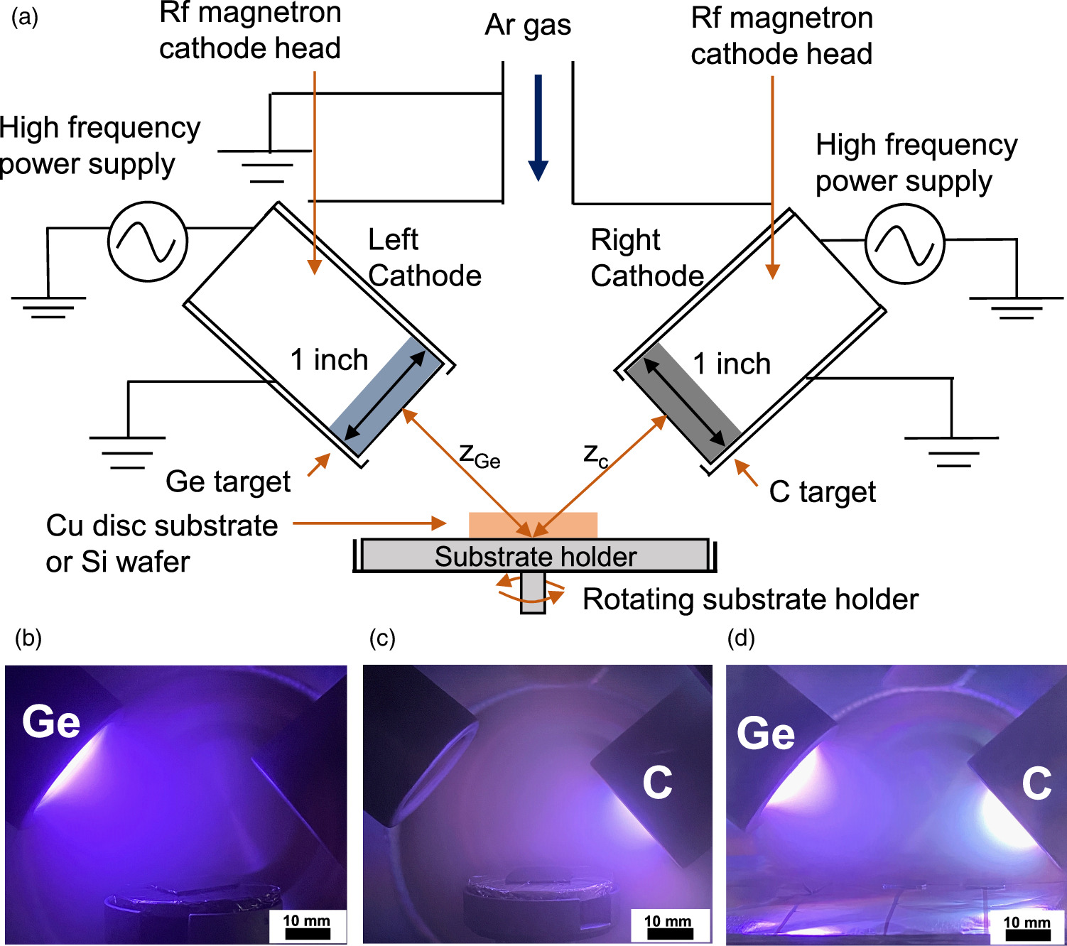
Fig. 1. (a) Experimental setup for RF magnetron plasma sputtering. Photographs of sputtering plasma for fabricating (b) Ge films, (c) C films, and (d) Ge/C mixed films.
Download figure:
Standard image High-resolution imageFigures 2(a) and 2(b) show surface SEM images of Ge and C monolayer films, respectively. Nanostructures on Ge and C were clearly observed for both films under a high-Ar-pressure sputtering condition at 500 mTorr. The average diameters of the nanograins were 20.4 and 13.9 nm for the Ge and C films, respectively. Figures 2(c) and 2(d) show Raman spectra of the nanostructured Ge and C films, respectively. In the spectrum of the Ge film, a broad peak is observed at ∼270 cm−1; this peak was assigned to Ge–Ge bonds in the amorphous Ge (a-Ge) structure. In general, the amorphous structure has an advantage for the lithiation of Ge because Li+ ions can isotropically diffuse into a-Ge nanograins without any crystalline-face dependence. 22,23) Figure 2(d) shows Raman spectra of the nanostructured C films. Two broad peaks are observed at 1591 and 1342 cm−1; the signal at 1591 cm−1 is assigned to a G band attributed to HF E2g first-order graphite crystals (sp2 bonds), and the signal at 1342 cm−1 is attributed to a D band related to structural disorder and defects. The observed peak-intensity ratio between the D and G bands was 0.77, and the full-width at half-maximum of the G band was 64 cm−1, which is relatively broad. The features of the Raman spectrum are similar to those of the spectrum of common carbon black particles, which are added during the anode slurry coating process to enhance electrical conductivity. 24,25) The sputtered carbon nanograins are identified to have a structure similar to that of amorphous carbon. 5,24) We also measured the mass density of deposited Ge films and calculated their porosity, which were 4.28 g cm−3 and 19.4%, respectively, indicating a porous film structure. At a high pressure of 500 mTorr, nanoparticles could be synthesized in a gas-phase plasma and stacked on the substrate because a higher-density plasma is produced locally in front of the cathode sputtering target, resulting in a large amount of highly reactive excited Ge atoms and subsequent nucleation and growth of nanoparticles in the gas phase.
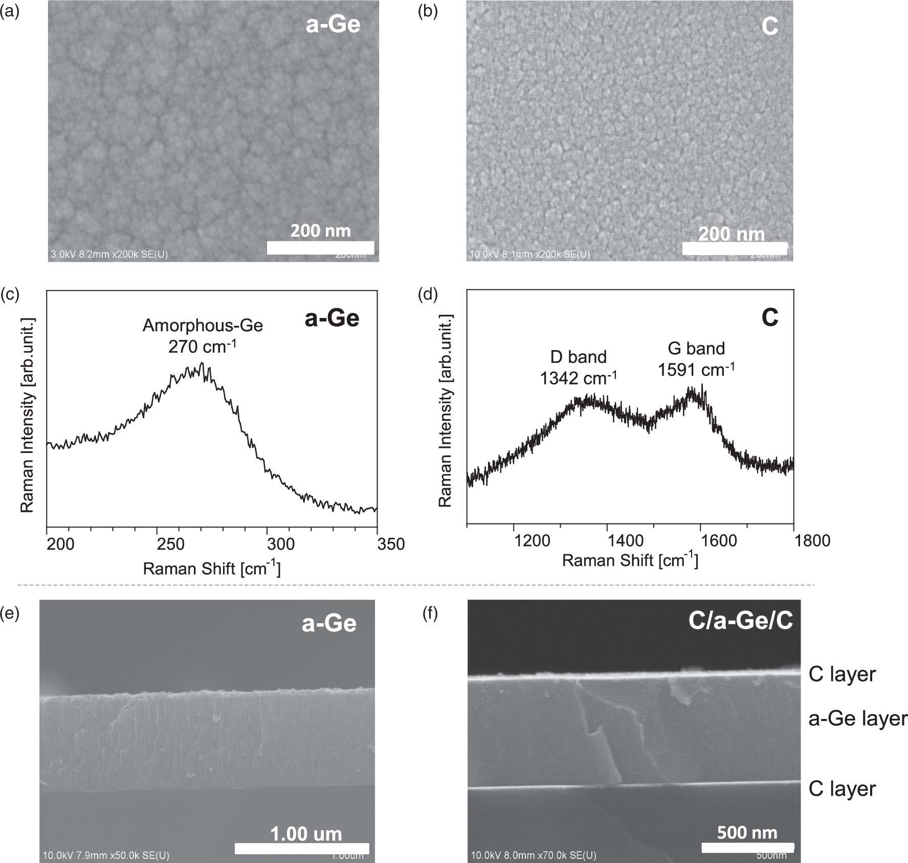
Fig. 2. SEM surface images of (a) Ge film and (b) C film. Raman spectra of (c) Ge film and (d) C film. SEM cross-sectional images of (e) Ge film and (f) C/Ge/C multilayer film.
Download figure:
Standard image High-resolution imageFigures 2(e) and 2(f) show cross-sectional SEM images of the a-Ge film and the C(top)/a-Ge(middle)/C(bottom) stacked multilayer film, respectively. The a-Ge layer has a dense structure and a thickness of 500 nm. In the C(top)/a-Ge(middle)/C(bottom) sandwich structure [Fig. 2(f)], thin amorphous-like C layers with thicknesses of 15 and 25 nm were deposited at the bottom and top of the nanostructured a-Ge film, respectively, by repeating the deposition process shown in Figs. 1(b) and 1(c).
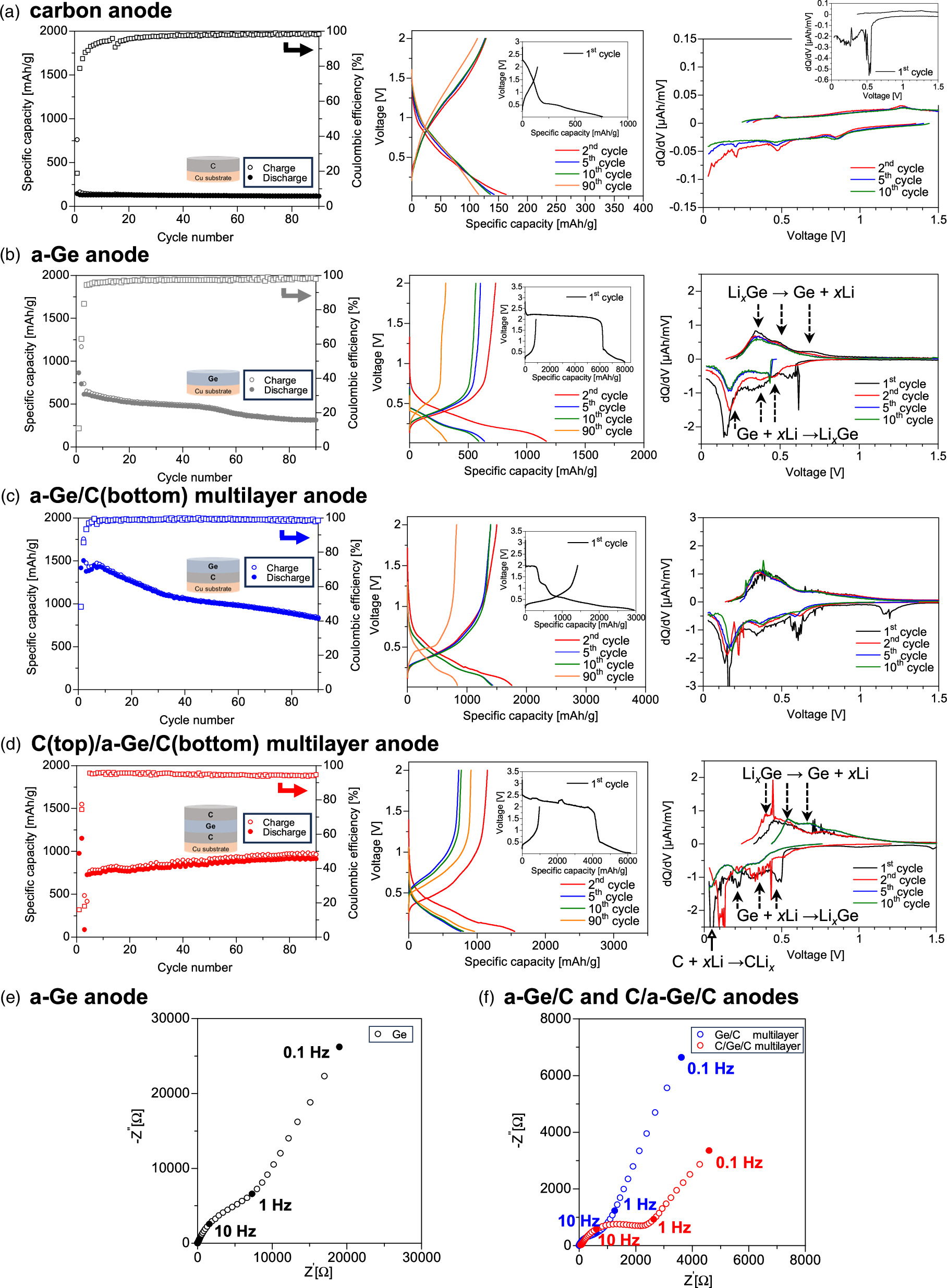
Figures 3(a)–3(d) show the gravimetric capacity of the sputtered carbon anode, a-Ge anode, a-Ge/C(bottom) multilayer anode, and C(top)/a-Ge(middle)/C(bottom) multilayer anode, respectively, as a function of the number charge–discharge cycles. A Coulomb efficiency greater than 90% was achieved within the first 10 cycles for all of the cells, as shown in the corresponding voltage profiles (middle graph).

Fig. 3. Charge–discharge capacity, charge–discharge voltage curves, and corresponding dQ/dV curves for LIBs with (a) C anode, (b) a-Ge anode, (c) a-Ge/C multilayer anode, and (d) C/a-Ge/C multilayer anode. Nyquist plots for (e) a-Ge anode, (f) C/a-Ge multilayer anode, and C/a-Ge/C multilayer anode, as obtained by electrochemical impedance spectroscopy, before charge–discharge process.
Download figure:
Standard image High-resolution imageThe differential capacity (dQ/dV) curve for an a-Ge anode [Fig. 3(b), right] shows three distinct peaks at 0.43–0.46, 0.38, and 0.18 V in the charging cycle (negative value); these peaks are attributed to the Li-alloying reaction in which a-Ge is transformed into Lix Ge. 8,19,26) In the discharging cycle (positive value), three peaks are observed at 0.36, 0.52, and 0.70 V, which indicates delithiation of Lix Ge to a-Ge. 7,19,27) Here, a noisy signal in the dQ/dV curve and a plateau region at ∼2.5 V in the voltage profile were observed in the first charging process; these observations are related to the formation of a solid-electrolyte-interface (SEI) layer by reaction between the a-Ge surface and the organic electrolyte. 19) For the C(top)/a-Ge(middle)/C(bottom) multilayer anode shown in the right graph of Fig. 3(d), we observed an interesting difference between the dQ/dV curves and those for the a-Ge single-layer anode: a new peak at a low voltage of 0.05 V was clearly observed in 5 and 10 cycles in the charging period (negative value). This new peak is caused by the intercalation reaction of Li+ ions into carbon, 28,29) indicating that the thin top or bottom C layers also slightly contribute to Li storage in the battery.
In the charge–discharge cycle characteristics of the LIBs, the cell with a sputtered amorphous-like C anode showed a low gravimetric capacity of 114 mAh g−1 after 90 cycles; however, a high capacity retention of 90% for 6–90 cycles is observed in Fig. 3(a), where the capacity retention was calculated for cycles with a Coulomb efficiency greater than 90%. By contrast, the three cells with the a-Ge, a-Ge/C(bottom), and C(top)/a-Ge(middle)/C(bottom) anodes showed much higher initial capacities of 864, 1417, and 976 mAh g−1, respectively, compared with 143 mAh g−1 for the C-anode cell. We observed a distinct difference in capacity degradation among the three types of a-Ge anodes: the C(top)/a-Ge(middle)/C(bottom) anode showed no capacity fading even after 90 cycles [Fig. 3(d)], whereas the capacity retention of the a-Ge and a-Ge/C(bottom) anodes was 50% for 4–90 cycles [Fig. 3(b)] and 60% for 3–90 cycles [Fig. 3(c)], respectively. As a result, the a-Ge, a-Ge/C, and C/a-Ge/C anodes achieved capacities of 309, 825, and 910 mAh g−1 after 90 cycles, respectively, and the C/a-Ge/C sandwiched structure achieved both a high capacity and high capacity retention.
The capacity retention markedly increased when the nanostructured carbon film was placed on the top side of the Ge material [Fig. 3(d)]. This result is attributed to stable SEI layers forming in the C/a-Ge/C anode. In general, SEI formation on a Ge active material is a dynamic process of bond breaking and reforming because of the volume changes during charge–discharge cycles. 5,30) Here, the inner layer of SEI on the Ge surface consists of compounds such as Lix GeOy , Lix Ge, Li2O, and LiF. 31) The breaking and reforming process leads to an increase in the size of the SEI region on the Ge surface, resulting in a huge irreversible capacity as well as high active Li loss and a continuous increase in interfacial resistance upon charge–discharge, which causes rapid capacity fading 5,30) in an a-Ge cell [Fig. 3(b)]. However, surface capping of the Ge active material with carbon nanograins would prevent the formation of an unstable and thick SEI layer on the Ge. 5,32,33) Here, SEI layers in C/a-Ge/C anode would be formed mainly on the top carbon surface and at interfaces between C and Ge layers. The middle Ge layer is mechanically fixed in-plane by the top carbon layer, and the stability of the SEI layer on Ge is markedly improved. The SEI layer on the carbon surface, by contrast, is quite stable during repeated charge–discharge cycles because the top carbon layer exhibits little volume expansion by lithiation. The inner layer of the SEI on the carbon surface is composed of compounds such as Li2CO3, Li2O, and LiF, 30,31) and appropriate carbon oxidation could contribute to stable cycle performance. 34) The mechanical and chemical effects of the top carbon layer lead to high capacity retention in the C/Ge/C structure [Fig. 3(d)].
The C/a-Ge/C anode has two interfaces between the C and Ge layers, leading to a higher internal resistance than in Ge and Ge/C anodes. This might be responsible for the decrease in Coulomb efficiency to 18% and the increase in the overpotential to 0.5 V when the C-rate was increased from 0.02 to 0.1 at the 3rd cycle [Fig. 3(d)]. In the Ge and a-Ge/C cells, the internal resistance gradually increases during repeated cycling because of the unstable SEI layer on the Ge anode surface, which results in a decrease in capacity and an increase in the overpotential after 90 cycles [Figs. 3(b) and 3(c)].
Oxidation would proceed mainly on the surface of the anode film. The top carbon layer in the C/a-Ge/C cell plays an important role as a passivation layer for preventing oxidation of the active Ge material, which results in a capacity loss because the theoretical reversible capacities of GeO and GeO2 are 1356 and 1100 mAh g−1, respectively. 14) The penetration of the electrolyte into the film is also important for promoting deep diffusion of Li+ ions into the Ge anode. The electrolyte gradually soaks into the entire Ge film with 19.4% porosity; 35) we therefore started the measurement of the cycle performance 24 h after fabricating the cell.
Nyquist plots for a-Ge monolayer and a-Ge/C(bottom) and C(top)/a-Ge(middle)/C(bottom) multilayer anodes [Figs. 3(e) and 3(f)], as obtained by electrochemical impedance spectroscopy (0.1 Hz to 100 kHz) before charge–discharge cycling, show semicircles in the HF region and straight lines in the low-frequency region. Here, the measurements were performed at the open-circuit voltage (2.9, 3.2, and 1.7 V for the Ge, Ge/C, and C/Ge/C cells, respectively). The voltage was higher than the lithiation/delithiation voltage for Ge; the semicircle in the HF region therefore corresponds mainly to electronic resistance. The electronic resistance for the developed multilayer anodes was substantially lower than that for the a-Ge monolayer anode. The insertion of the bottom carbon layer strengthens adhesion and attachment between the Cu electrode and a-Ge active material and improves electron transfer from the Cu current collector to the Ge material. 6,36) The lower electronic resistance also results in a higher discharge capacity for the multilayer anode [Figs. 3(c) and 3(d)].
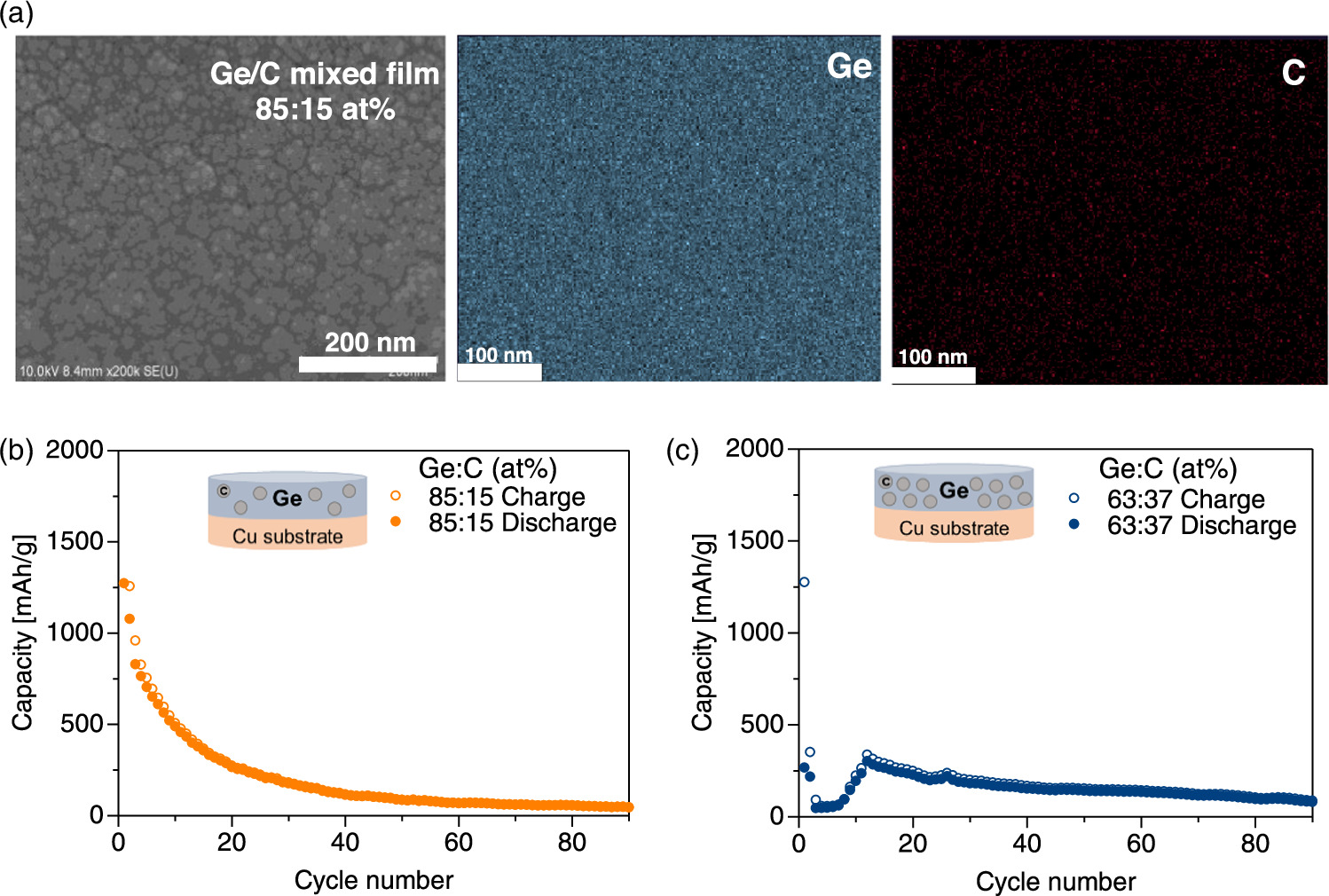
We also fabricated GeC mixed films using co-sputtering of Ge and C targets, as shown in Fig. 1(d), where sputtering process parameters such as the RF power and gas pressure were approximately the same for the monolayer and multilayer films (Fig. 2). As shown in the SEM surface image in Fig. 4(a), a nanostructured GeC film with an average grain size of 19.0 nm was fabricated, and analysis by energy-dispersive X-ray spectroscopy (EDX) indicated a carbon content of 15 at% in the Ge film. The right side of Fig. 4(a) shows EDX mappings of Ge and C atoms with respect to the SEM-image area. The chemical composition is homogeneous, and carbon is uniformly distributed without segregation in the a-Ge film.
Fig. 4. (a) SEM surface image of the GeC mixed film and SEM–EDX mappings of Ge and C with respect to SEM area. Cycle performance of GeC mixed anodes with C content of (b) 15 at% and (c) 37 at%.
Download figure:
Standard image High-resolution image
Figure 4(b) shows the cycle performance of LIBs with the GeC mixed anode. The GeC mixed anode showed a maximum discharge capacity of 1118 mAh g−1 at the 6th cycle. However, the capacity rapidly decreased for 10–20 cycles, resulting in a low discharge capacity of 56 mAh g−1 after 90 cycles. We also fabricated films with higher carbon contents, where the carbon content was increased from 15 at% to 37 at%.
When the C-rate was increased from 0.02 to 0.1 at the 3rd cycle, the capacity of the high-carbon-content cell suddenly decreased [Fig. 4(c)]. A high carbon content leads to abundant Ge/C interfaces in the anode, resulting in higher internal resistance and a subsequent decrease in capacity. However, after 90 cycles, no substantial difference in capacity was observed between the anodes with high and low carbon contents. The connection between C and Ge atoms is insufficient in our binder-free process, and strong physical and chemical Ge–C bonding is required in the GeC mixed films.
In conclusion, various nanostructured Ge–C composite anodes with 10–20 nm nanograins were fabricated using a binder-free process involving plasma sputtering at a high Ar pressure of 500 mTorr. By comparison with the Ge and C mixed anode, the C/a-Ge/C multilayer anode showed much better performance and achieved a high discharge capacity of 910 mAh g−1 with no capacity fading after 90 cycles. A carbon stacking structure of Ge active material, which exhibits a large volume expansion, is effective for realizing high cycle stability in next-generation LIBs.