
Abstract
A well-ordered molecular arrangement is a necessary condition for "band transport" in molecular semiconductor materials, and thus it is important for donor–acceptor molecular junctions for applications in advanced organic optoelectronic devices. In this study, the heteroepitaxial growth of an acceptor material C60 on a single-crystal (001) surface of dinaphtho[2,3-b:2',3'-f]thieno[3,2-b]thiophene (DNTT), a representative high-mobility donor material, is demonstrated. Surface X-ray diffraction analysis indicated spontaneous alignment of the nearest-neighbor molecular direction of the C60 crystallites uniquely to the a-axis of the DNTT.
Export citation and abstract BibTeX RIS
"Band transport" in organic semiconductors requires a well-ordered molecular arrangement, which is essential for organic electronic devices potentially competing with inorganic counterparts. 1–4) The material used in this study, dinaphtho[2,3-b:2',3'-f]thieno[3,2-b]thiophene (DNTT, Fig. 1 inset), is a prominent example, having considerable charge carrier mobility surpassing 1 cm2Vs−1 5–8) and widely-dispersed intermolecular electronic bands. 9,10) Therefore, it has been used as a benchmark molecular semiconducting material in the development of advanced electronic devices. 11–15) For optoelectronic devices such as organic photovoltaics, which generally require heterojunctions of donor- and acceptor-type compounds, DNTT is used as a donor molecule. 16–21) For instance, the combination of DNTT with C60 as a representative acceptor molecule is known to exhibit photovoltaic characteristics. 16,18) Compared to unsubstituted donor acenes, DNTT is regarded as more advantageous, owing to its chemical stability against (photo-)oxidation reactions. 22,23)
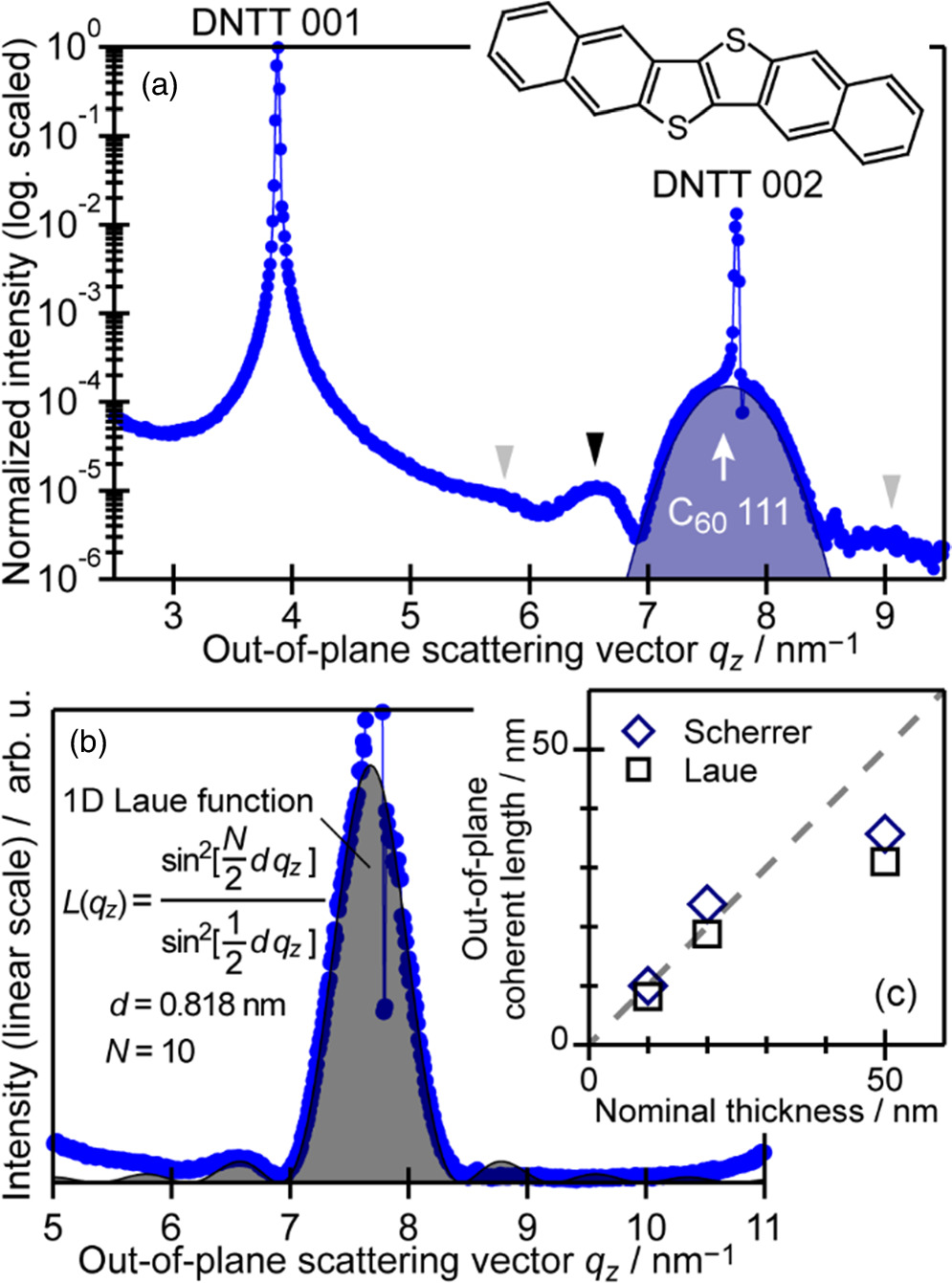
Fig. 1. (a) Out-of-plane XRD profile of a DNTT single-crystal sample covered with 10 nm thick C60, where the vertical axis is represented in logarithmic scale. The contribution of the C60 111 reflection is approximated by a Gaussian curve, as indicated with the blue parabola, accompanied by Laue oscillation (marked by wedge symbols). (Inset) Molecular structure of DNTT. (b) Out-of-plane XRD spot profile for the C60 111 reflection of 10 nm thick C60 on single-crystal DNTT. The gray-shaded curve represents a Laue function of N = 10 centered at qz = 7.68 nm−1 (d = 0.818 nm). (c) Out-of-plane coherent length L derived from the Laue functions as L = N × d (squares) and from the Scherrer equation (diamonds) plotted as a function of the nominal C60 thickness.
Download figure:
Standard image High-resolution imageIn this study, well-ordered molecular heterojunctions were constructed by stacking C60 molecules on the single-crystal (001) surface of DNTT. Despite significant dissimilarities in crystallographic symmetry and lattice constants, the hexagonal arrangement of C60 in the (111) orientation of its bulk face-centered cubic (fcc) crystal structure grows epitaxially on a rectangular surface lattice of monoclinic DNTT, which can be understood from paradigms known as "van der Waals epitaxy" or "weak epitaxy." 24–26) Precise analysis using surface X-ray diffraction techniques reveals a unique inter-lattice relationship at this molecular heterojunction, in which the nearest-neighbor molecular direction of C60 is aligned parallel to the a -axis of DNTT. A plausible factor for this alignment of C60 molecules is similar to the previously reported epitaxial C60 and perfluoropentacene on the single-crystal pentacene. 27–29)
Single crystals of DNTT were produced using a horizontal physical vapor transport technique in a nitrogen stream at atmospheric pressure. 30) Plate-shaped crystals were collected under an ambient atmosphere and fixed on Si wafer pieces by electrostatic force to prepare "single-crystal substrates." C60 was deposited onto the single-crystal DNTT under ultra-high vacuum conditions (typically 1 × 10⁻⁷ Pa). The deposition rate of C60 was finely controlled at 0.02 nm s−1. Although the sample temperature was not intentionally controlled during C60 deposition, it was considered to be RT. The surface morphology of the heterojunction samples was observed using non-contact mode atomic force microscopy (nc-AFM).
The crystallographic structure of the heterojunctions was elucidated using out-of-plane X-ray diffraction (XRD) and grazing-incidence X-ray diffraction (GIXD) at BL19B2, BL46XU, and BL13XU of SPring-8. Two types of X-ray detectors were used for the experiments: a two-dimensional pixel detector (PILATUS-300K) for two-dimensional GIXD (2D-GIXD) and a scintillation counter for out-of-plane XRD and GIXD spot profile analyses. The X-ray glancing angle was set to 0.12° for the GIXD experiments. For the 2D-GIXD measurements, diffraction images were collected during azimuthal rotation of the sample over 360°, and the 2D detector was placed perpendicular to the incident X-rays at approximately 175 mm from the sample rotation center. Details of the measurement setup can be found elsewhere. 27) In these experiments, the X-ray wavelength was fixed at 0.100 nm and the measurements were conducted under an ambient atmosphere at RT.
Figure 1(a) shows the X-ray intensity of a DNTT single-crystal sample covered with 10 nm thick C60 plotted as a function of the out-of-plane scattering vector qz . Sharp peaks at qz = 3.88 and 7.75 nm−1 correspond to the 001 and 002 reflections, respectively, of the single-crystal DNTT, 5) indicating that the single-crystal DNTT substrates are in c *-axis orientation. It is worth noting that the interlayer spacing (1.622 nm) derived from the 004 spot agrees with the reported bulk crystal structure of DNTT, and any additional features assignable to the thin-film phase of DNTT 31) are not found (Supplemental Materials Fig. S1). Compared to the 001 peak, the spot profile of the 002 reflection exhibits a bell-shaped curve. This relatively broad feature centered at qz = 7.68 nm−1 is attributable to the 111 reflection of C60 in the fcc structure. 32) This indicates that fcc-C60 crystallites grew in the (111) orientation on the (001) surface of the DNTT single crystals. As shown in Fig. 1(a), the C60-derived feature is well reproduced by a Gaussian curve with a FWHM of 0.64 nm−1. This width corresponds to a crystalline coherent length of 10.0 nm based on a formula given in Ref. 33. In addition, the C60 111 reflection is accompanied by several side peaks, which can be reproduced by the one-dimensional Laue function of the crystalline repeating number N = 10 [Fig. 1(b)]. These results indicate that crystalline coherence is fulfilled over the entire thickness range of the 10 nm thick C60 overlayers on DNTT, which is the case for RT-grown C60 on single-crystal pentacene, 34) and the crystalline thickness is quite uniform over the surface, as also suggested by AFM observations (Fig. S2). It is worth noting that, as suggested in Fig. 1(c), the out-of-plane crystalline coherent length of C60 is shorter than the nominal thickness for a 50 nm thick C60-covered sample, similar to the case of a rubrene derivative on single-crystal rubrene, 35) while the substantial agreement of these two is satisfied for a 20 nm thick sample (Fig. S3).
Figure 2(a) shows the 2D-GIXD results for the 10 nm C60-covered DNTT single-crystal sample, for which the image was obtained by integrating data from 720 2D-GIXD snapshots taken at 0.5° intervals of the sample azimuthal angle during 360° rotation, and the background signal was subtracted for enhancement of the image contrast (see Fig. S4). While most of the intense signals can be assigned to diffractions spots of the (001)-oriented DNTT (indicated by diamond-shaped marks in Fig. S5), several additional spots are attributable to C60, e.g., spots at (qxy
, qz
) = (12.5 nm−1, 0 nm−1) indicated with an arrow with a circle mark corresponds to six  -equivalent diffractions of the (111)-oriented fcc-C60.
28) This also confirms the growth of C60 crystallites in the (111) orientation on DNTT.
-equivalent diffractions of the (111)-oriented fcc-C60.
28) This also confirms the growth of C60 crystallites in the (111) orientation on DNTT.
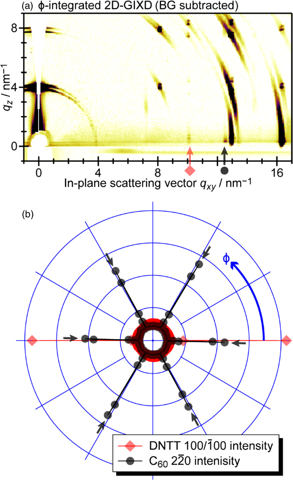
Fig. 2. (a) Azimuthally-integrated 2D-GIXD image of the 10 nm thick C60-covered DNTT single-crystal sample. Arrows indicate (qxy
, qz
) positions for the 100 and  spots of the (001)-oriented DNTT and the
  and five equivalent spots of the (111)-oriented fcc-C60. (b) Polar plot of the 2D-GIXD intensity (radial direction in a linear scale) at and around (qxy
, qz
) positions corresponding to the 100/
and five equivalent spots of the (111)-oriented fcc-C60. (b) Polar plot of the 2D-GIXD intensity (radial direction in a linear scale) at and around (qxy
, qz
) positions corresponding to the 100/ spots of DNTT (diamonds) and the
  -equivalent spots of C60 (circles) plotted as a function of ϕ (azimuthal direction). The peak positions of C60 are indicated with arrows.
Download figure:
Standard image High-resolution imageThe 2D-GIXD signal intensities of 3 × 25 pixels including the (qxy
, qz
) position (10.16 nm−1, 0.44 nm−1) and those of 5 × 13 pixels including (qxy
, qz
) = (12.46 nm−1, 0 nm−1) are plotted as a function of the in-plane azimuthal angle ϕ in Fig. 2(b), where the former corresponds to the 100 and  diffractions of DNTT [indicated with an arrow with a diamond mark in Fig. 2(a)] and the latter corresponds to the
  -equivalent diffractions of C60. The sample azimuthal orientation where the DNTT 100 diffraction is detected is defined to be ϕ = 0° hereafter. C60
 -equivalent spots are present only six times at 60° intervals. Common to all the five individual samples examined in the present study, the C60
 -equivalent spots appear at ϕ = (−1.15 ± 0.5)° + n × 60° (n = 1, 2, ⋯, 6) as summarized in Fig. S6. The C60-derived diffraction intensity appears only at specific azimuthal orientations at 60° intervals, indicating that the C60 crystallites are uniformly aligned along a specific axis of the DNTT (001) surface; in other words, C60 grew epitaxially on the single-crystal DNTT substrates.
27,28)
-equivalent spots appear at ϕ = (−1.15 ± 0.5)° + n × 60° (n = 1, 2, ⋯, 6) as summarized in Fig. S6. The C60-derived diffraction intensity appears only at specific azimuthal orientations at 60° intervals, indicating that the C60 crystallites are uniformly aligned along a specific axis of the DNTT (001) surface; in other words, C60 grew epitaxially on the single-crystal DNTT substrates.
27,28)
The inter-lattice relationship between the epitaxial C60 and the single-crystal DNTT (001) surface can be deduced from the ϕ-dependence of the C60
 -equivalent spots based on a procedure reported previously.
36) In brief, an angle difference δ from the reference axis of the epitaxial C60 with respect to that of DNTT can be deduced from the ϕ value where a C60-derived diffraction spot appears as δ + φ'C − φ'D = −ϕ. Here, φ'C is an in-plane angle of the incident X-ray wave vector at which the C60-derived topical spot fulfills the diffraction condition, and φ'D is that for a DNTT-derived diffraction spot. The incident X-ray orientation angle φ' is taken with respect to the reference axis of each material, and φ' for a diffraction spot of
q
≡ (qxy
cosα, qxy
sinα, qz
) is estimated as φ' = α − cos−1[|
q
|2/2kqxy
], where α is the argument angle of the reciprocal point corresponding to the topical diffraction and k is the magnitude of the X-ray wave vector (in this case k = 2π/0.100 nm−1). In this study, DNTT 100 and C60
-equivalent spots based on a procedure reported previously.
36) In brief, an angle difference δ from the reference axis of the epitaxial C60 with respect to that of DNTT can be deduced from the ϕ value where a C60-derived diffraction spot appears as δ + φ'C − φ'D = −ϕ. Here, φ'C is an in-plane angle of the incident X-ray wave vector at which the C60-derived topical spot fulfills the diffraction condition, and φ'D is that for a DNTT-derived diffraction spot. The incident X-ray orientation angle φ' is taken with respect to the reference axis of each material, and φ' for a diffraction spot of
q
≡ (qxy
cosα, qxy
sinα, qz
) is estimated as φ' = α − cos−1[|
q
|2/2kqxy
], where α is the argument angle of the reciprocal point corresponding to the topical diffraction and k is the magnitude of the X-ray wave vector (in this case k = 2π/0.100 nm−1). In this study, DNTT 100 and C60
 -equivalent diffraction spots were used for the analyses, and the [100] and [
 ] directions are defined as the reference axes for the DNTT (001) surface and (111)-oriented C60 crystallites, respectively, denoted as
a
D and
x
C hereafter. From the above equation, φ'D is calculated to be −85.356° from α = 0°, |
q
| = 10.165 nm−1, and qxy
= 10.155 nm−1 for the DNTT 100 diffraction. For C60
] directions are defined as the reference axes for the DNTT (001) surface and (111)-oriented C60 crystallites, respectively, denoted as
a
D and
x
C hereafter. From the above equation, φ'D is calculated to be −85.356° from α = 0°, |
q
| = 10.165 nm−1, and qxy
= 10.155 nm−1 for the DNTT 100 diffraction. For C60
 φ'C is calculated to be −114.308° from α = −30° and |
q
| = qxy
= 12.463 nm−1. Therefore, the experimental ϕ value of (−1.15 ± 0.5)° for the C60
φ'C is calculated to be −114.308° from α = −30° and |
q
| = qxy
= 12.463 nm−1. Therefore, the experimental ϕ value of (−1.15 ± 0.5)° for the C60
 diffraction leads to δ = (30.1 ± 0.5)°. This strongly suggests that the angle difference between
a
D and
x
C is approximately 30°; in other words, the [
diffraction leads to δ = (30.1 ± 0.5)°. This strongly suggests that the angle difference between
a
D and
x
C is approximately 30°; in other words, the [ ] direction of C60 is aligned with the
a
-axis of the single-crystal DNTT. The inter-lattice relationship derived from the above discussion is illustrated in Fig. 3(a).
] direction of C60 is aligned with the
a
-axis of the single-crystal DNTT. The inter-lattice relationship derived from the above discussion is illustrated in Fig. 3(a).
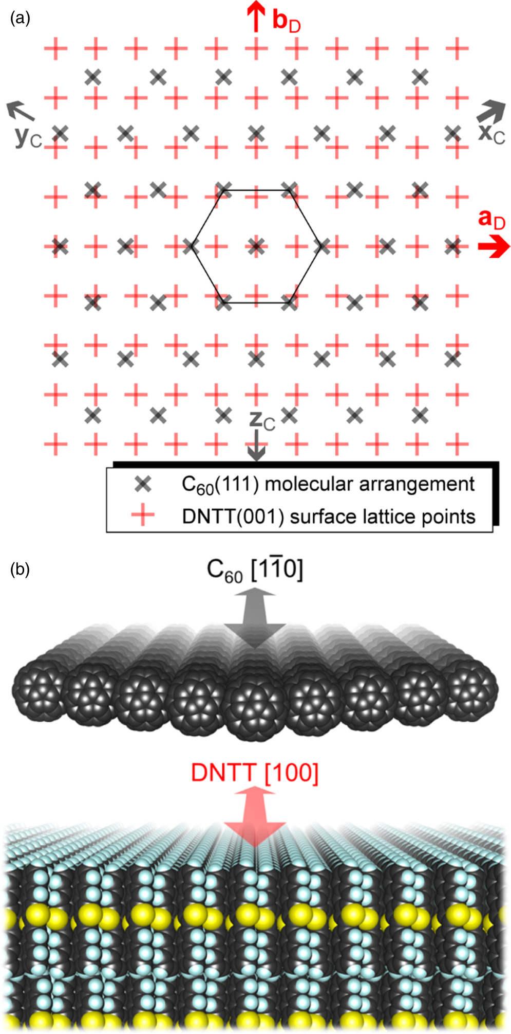
Fig. 3. (a) Schematic diagram representing the inter-lattice relationship of the epitaxial C60 (× marks) on the single-crystal (001) surface of DNTT (+ marks). In-plane orientations of the reference axes (aD and xC) within the DNTT(001) and C60(111) surfaces are indicated as thick arrows, while orientations of the secondary axes (denoted as bD for DNTT and yC and zC for C60) are also displayed by thin arrows. The hexagon indicates the six-fold molecular arrangement of a molecular layer of the (111)-oriented fcc-C60. (b) Schematic drawings of the molecular arrangements at the contacting layers of the C60/DNTT heterojunction. The molecular arrangements were drawn using VESTA 37) based on cif files provided in Refs. 5, 32.
Download figure:
Standard image High-resolution image
On the (111) surface of fcc-C60, the molecules form a hexagonal arrangement within the first molecular layer, and the nearest-neighbor directions of the C60 molecules correspond to the 〈 〉 axes. In the case of the epitaxial growth of C60 and perfluoropentacene on the single-crystal pentacene surface,
28,29) the nearest-neighbor directions of the overlayer molecules align along the [
〉 axes. In the case of the epitaxial growth of C60 and perfluoropentacene on the single-crystal pentacene surface,
28,29) the nearest-neighbor directions of the overlayer molecules align along the [ ] axis of the pentacene, which is predicted to be the direction where surface diffusion of the adsorbed molecules occurs most frequently.
38) Although the migration behavior of C60 on the DNTT single-crystal surface is unknown, frequent surface diffusion along the [100] direction seems likely because of the atomic-scale ridge and trough structure running in this direction, as illustrated in Fig. 3(b). Therefore, it is suggested that the present crystallographic orientation of the epitaxial C60 on single-crystal DNTT is determined by the same principle as that described previously for C60 on pentacene.
] axis of the pentacene, which is predicted to be the direction where surface diffusion of the adsorbed molecules occurs most frequently.
38) Although the migration behavior of C60 on the DNTT single-crystal surface is unknown, frequent surface diffusion along the [100] direction seems likely because of the atomic-scale ridge and trough structure running in this direction, as illustrated in Fig. 3(b). Therefore, it is suggested that the present crystallographic orientation of the epitaxial C60 on single-crystal DNTT is determined by the same principle as that described previously for C60 on pentacene.
Finally, possible photo-response of the topical molecular junction is discussed. Mori and Takimiya reported a superior power conversion efficiency of solar cells with an exciton dissociating interface between crystalline thin films of DNTT and C60 overlayers produced by sequential vacuum deposition in comparison to pentacene-C60 solar cells fabricated in the same manner. 16) They attributed a plausible origin of the better cell performance to a higher crystalline order of the DNTT thin-film which leads to more efficient charge carrier transport characteristics. Considering that not only the single-crystal DNTT yields an ideal hole transporting efficiency for this species but also much improvement of electron conduction can be expected for C60 in a uniform crystalline orientation, the present epitaxial C60/DNTT heterojunction has the potential to lead to the development for highly-efficient photovoltaic applications. On the other hand, to achieve a mature understanding of solar cell performance, knowledge of the electronic energy level alignment at the exciton dissociating interface is also indispensable. While photoemission experiments unveiled the energy level diagram and the fulfillment of the Schottky–Mott limit for the case of epitaxial C60 on the single-crystal pentacene, 39) it remains a challenge for demonstration of the photoelectron spectroscopy measurements on the epitaxial C60 on the single-crystal DNTT samples.
In summary, the epitaxial growth of C60 on single-crystal DNTT (001) surfaces was demonstrated using surface XRD measurements. The out-of-plane XRD results indicate that C60 forms (111)-oriented fcc crystallites with a uniform coherent thickness on DNTT. In-plane azimuthal analysis of the 2D-GIXD data revealed an inter-lattice relationship between the epitaxial C60 and the single-crystal DNTT (001) surface in which the nearest-neighbor direction of the C60 molecules uniquely aligns along the crystalline a -axis of DNTT.
Acknowledgments
This work was conducted as the Joint-Studies-Programs of IMS [S-20-MS-0007, S-21-MS-0010, and 22IMS1209] and was performed under the approval of JASRI [2020A1627, 2021A1629, and 2022A1324]. Financial support from the JSPS-KAKENHI [Grant Nos. JP22H02055 and JP21H05405], the Research Foundation for the Electrotechnology of Chubu (REFEC), The Shimadzu Science Foundation, and the Futaba Foundation are gratefully acknowledged.
Supplementary data (0.6 MB PDF)