
Abstract
The effects of a process that minimizes oxidation of SiC on the channel mobility of heavily doped 4H-SiC (0001), (11 0) and (1
 00) metal-oxide-semiconductor field-effect transistors (MOSFETs) were investigated. High field-effect mobilities were obtained for these MOSFETs even when the acceptor concentration of the p-body (NA) exceeded 1 × 1018 cm−3. The field-effect mobility for the (0001) MOSFETs reached 25 cm2 V−1 s−1 (NA = 1 × 1018 cm−3). The fabricated (11
 0) and (1
 00) MOSFETs showed very high channel mobilities of 125 cm2 V−1 s−1 (NA = 1 × 1018 cm−3) and 80 cm2 V−1 s−1 (NA = 5 × 1018 cm−3), respectively.
Export citation and abstract BibTeX RIS
Silicon carbide (SiC) metal-oxide-semiconductor field-effect transistors (MOSFETs) have attracted much attention as high-efficiency power devices. 1–4) However, the performance of SiC MOSFETs has been far from their full potential, which is determined by the physical properties of SiC, because of the low channel mobility due to the high density of states at the SiC/SiO2 interface 5–13) and the low drift mobility in the inversion layer. 14–27) Although the channel mobility can be improved by annealing in nitric oxide (NO) after the formation of a gate stack, the high channel resistance still dominates the total on-resistance for medium-voltage (∼1 kV) SiC MOSFETs. To overcome this problem, most commercial SiC MOSFETs utilize a very short channel structure. However, for a sub-micron channel length, short-channel effects may occur depending on the acceptor concentration in the p-body region. 28–32) Further reduction in on-resistance cannot be achieved only by reducing the channel resistance through shortening the channel length. Thus, a reduction in the interface state density (Dit) is necessary for further improvement of on-resistance in SiC MOSFETs. 33–36)
We have recently found that oxidation of SiC induces interface defects and that H2 etching prior to oxide film formation is a key to obtaining a high-quality 4H-SiC (0001)/SiO2 interface. 37–39) Three factors are important for obtaining a high-quality interface: (i) H2 etching of SiC surface, (ii) SiO2 formation without oxidation of SiC, and (iii) interface nitridation. A very low Dit (2–6 × 1010 cm−2 eV−1) and high channel mobility (>80 cm2 V−1 s−1) have been obtained using a process that includes these steps.
Although the above process reduces the density of interface defects and enhances channel mobility, the acceptor concentration (NA) of the p-body for the reported MOSFET was 1 × 1015 cm−3, which is extremely low compared with that used for practical MOSFETs. In addition, MOSFETs on other faces than (0001) have not been investigated. High channel mobilities (>90 cm2 V−1 s−1) have been obtained for (11 0) and (1
 00) MOSFETs with the gate insulator formed by oxidation and NO annealing.
40) These faces are promising for the vertical sidewalls of trench-type SiC MOSFETs.
00) MOSFETs with the gate insulator formed by oxidation and NO annealing.
40) These faces are promising for the vertical sidewalls of trench-type SiC MOSFETs.
In this study, we investigate the effects of the process that minimizes oxidation of SiC on the channel mobility of heavily doped 4H-SiC (0001), (11 0), and (1
 00) MOSFETs (1 × 10¹⁷–5 × 1018 cm−3). As in the case of the (0001) face, this process effectively reduced Dit for the SiC/SiO2 structure fabricated on (11
 0) and (1
 00) faces. The fabricated (0001), (11
 0), and (1
 00) MOSFETs showed a marked improvement in channel mobility.
For characterization of Dit, n-type MOS capacitors were fabricated on n-type 4H-SiC (0001), (11 0), and (1
 00) epilayers on n-type substrates. The SiC (11
 0) and (1
 00) substrates were prepared by vertically slicing ingots grown on (000
 ). The doping concentrations of the epilayer were 5 × 10¹⁵ − 3 × 1016 cm−3. After RCA cleaning, samples were etched in H2 ambient at 1350 °C and 0.1 MPa for 8–15 min. The gate oxides were formed via plasma-enhanced chemical vapor deposition (PECVD) at 400 °C, which resulted in an oxide thickness of 30–35 nm. For comparison, we also prepared MOS capacitors with oxides formed via dry oxidation at 1300 °C. Finally, NO annealing (1250 °C, 70 min) was performed. Here, "H2-CVD-NO" denotes samples with a gate oxide formed via H2 etching, SiO2 deposition, and NO annealing, and "Ox-NO" denotes samples with a gate oxide formed via thermal oxidation and NO annealing. The gate material was Al.
Lateral n-channel MOSFETs were fabricated on p-type 4H-SiC (0001), (11 0), and (1
 00) epilayers. The NA values for the p-type epilayers were 1 × 1017 cm−3 and 1 × 1018 cm−3 for (0001) and (11
 0) and 3 × 1017 cm−3 and 5 × 1018 cm−3 for (1
 00). The gate oxide was formed in the same manner as that for the MOS capacitors (thickness: 30–35 nm). Al electrodes were deposited onto the source and drain regions and ohmic contact annealing was conducted for 4 min at 400 °C. Gate electrodes were formed by Al deposition. The channel length and width of the MOSFETs were 100 μm and 170 μm, respectively.
Figure 1 shows the energy distributions of Dit near the conduction band edge (Ec) extracted using the high (1 MHz)-low method for the (0001), (11 0), and (1
 00) MOS capacitors. Compared with the Dit for the Ox-NO samples, that for the samples fabricated using the H2-CVD-NO process was significantly lower for all three faces. The Dit values (energy range of Ec − 0.2 eV to Ec − 0.5 eV) are as low as about 4–8 × 1010 cm−2 eV−1 for (0001) and 1–5 × 1010 cm−2 eV−1 for (11
 0) and (1
 00). In the figure, the obtained Dit values obtained on (1
 00) and (11
 0) are close to the detection limit of the high-low method (1–2 × 1010 cm−2 eV−1), and the Dit difference between on these faces observed in Fig. 1 is not conclusive.

Fig. 1. (Color online) Energy distribution of Dit extracted using the high (1 MHz)-low method for the (0001), (11 0), and (1
 00) MOS capacitors. Gate oxides were formed by "H2-CVD-NO" and "Ox-NO" processes.
Download figure:
Standard image High-resolution imageThe typical gate characteristics and field-effect mobility for the fabricated (0001) MOSFETs are shown in Fig. 2. The applied drain voltage was 0.1 V. The peak mobilities for the H2-CVD-NO devices are approximately twice as high as those for the Ox-NO devices for NA values of 1 × 1017 cm−3 and 1 × 1018 cm−3, although the threshold voltage of the H2-CVD-NO devices is slightly lower.

Fig. 2. (Color online) Transfer characteristics (a) and field-effect mobility (b) as a function of gate voltage for fabricated SiC MOSFETs on (0001). The acceptor concentrations of p-body are 1 × 1017 cm−3 and 1 × 1018 cm−3. Gate oxides were formed by "H2-CVD-NO" and "Ox-NO" processes.
Download figure:
Standard image High-resolution imageThe typical gate characteristics and field-effect mobility of the fabricated (11 0) and (1
 00) MOSFETs are shown in Figs. 3 and 4, respectively. As in the case of the (0001) MOSFETs, the channel mobility was improved by the H2-CVD-NO process. The channel mobility reached 125–130 cm2 V−1 s−1 for the (11
 0) MOSFETs and 80–112 cm2 V−1 s−1 for the (1
 00) MOSFETs. Compared with the Ox-NO process, the H2-CVD-NO process resulted in the channel-mobility enhancement by a factor of about 1.5 for the (11
 0) and (1
 00) MOSFETs with NA values of 1 × 1017 cm−3 and 3 × 1017 cm−3, respectively. The difference in the channel mobility between the Ox-NO and H2-CVD-NO MOSFETs greatly increases with increasing NA of the p-body. The channel mobility improvement is 6-fold for (11
 0) MOSFETs (NA = 1 × 1018 cm−3) and 100-fold for (1
 00) MOSFETs (NA = 5 × 1018 cm−3).
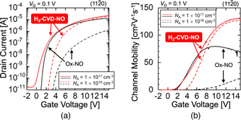
Fig. 3. (Color online) Transfer characteristics (a) and field-effect mobility (b) as a function of gate voltage for MOSFETs fabricated on (11 0). The acceptor concentrations of p-body are 1 × 1017 cm−3 and 1 × 1018 cm−3.
Download figure:
Standard image High-resolution image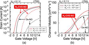
Fig. 4. (Color online) Transfer characteristics (a) and field-effect mobility (b) as a function of gate voltage for MOSFETs fabricated on (1 00). The acceptor concentrations of p-body are 3 × 1017 cm−3 and 5 × 1018 cm−3.
Download figure:
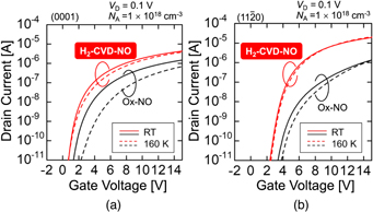
Standard image High-resolution imageTo investigate the main factor causing the mobility enhancement in the H2-CVD-NO process, the gate characteristics of the (0001) and (11 0) MOSFETs (NA = 1 × 1018 cm−3) were measured at 160 K and the results are shown in Fig. 5. For a quantitative discussion, the threshold voltage (Vth) is defined as the gate voltage at which the drain current reaches 1 × 10⁻⁷ A. It is known that the gate characteristics of the SiC (0001) MOSFETs with NO treatment show a clear increase in the threshold voltage and a decrease in channel mobility at lower temperature due to pronounced electron trapping at the SiC/SiO2 interface.
41) The Vth shift for the Ox-NO (0001) MOSFET from room temperature to 160 K was 2.8 V, the result of which is similar to the previous report.
41) In contrast, for the H2-CVD-NO (0001) device, the Vth shift was as small as 0.6 V. The peak channel mobility for the Ox-NO device decreased from 12 to 8 cm2 V−1 s−1 with lowering the temperature, whereas that for the H2-CVD-NO device slightly increased from 25 to 26 cm2 V−1 s−1. The fabricated (11
0) MOSFETs (NA = 1 × 1018 cm−3) were measured at 160 K and the results are shown in Fig. 5. For a quantitative discussion, the threshold voltage (Vth) is defined as the gate voltage at which the drain current reaches 1 × 10⁻⁷ A. It is known that the gate characteristics of the SiC (0001) MOSFETs with NO treatment show a clear increase in the threshold voltage and a decrease in channel mobility at lower temperature due to pronounced electron trapping at the SiC/SiO2 interface.
41) The Vth shift for the Ox-NO (0001) MOSFET from room temperature to 160 K was 2.8 V, the result of which is similar to the previous report.
41) In contrast, for the H2-CVD-NO (0001) device, the Vth shift was as small as 0.6 V. The peak channel mobility for the Ox-NO device decreased from 12 to 8 cm2 V−1 s−1 with lowering the temperature, whereas that for the H2-CVD-NO device slightly increased from 25 to 26 cm2 V−1 s−1. The fabricated (11 0) MOSFETs showed a trend similar to that for the (0001) MOSFETs. The Vth shift was 0.9 V for the Ox-NO device and 0.2 V for the H2-CVD-NO device. The channel mobility markedly increased, from 125 to 145 cm2 V−1 s−1 as the device was cooled from room temperature to 160 K, for the H2-CVD-NO device. These results indicate that Dit near Ec is substantially reduced in H2-CVD-NO MOSFETs, which is consistent with the results shown in Fig. 1.
Fig. 5. (Color online) Subthreshold characteristics of fabricated (a) (0001) and (b) (11 0) MOSFETs (Na = 1 × 1018 cm−3) at 300 and 160 K.
Download figure:
Standard image High-resolution image
The superior mobility in SiC(11 0) and (1
 00) MOSFETs compared with that in SiC (0001) MOSFETs fabricated with the conventional process (Ox-NO: oxidation followed by annealing in NO) is well known and has been ascribed to the lower Dit near the conduction band edge.
40) A similar logic will be valid in the case of the proposed process (H2-CVD-NO), as indicated in Figs. 1 and 5. The Dit values near the conduction band edge on SiC (11
00) MOSFETs compared with that in SiC (0001) MOSFETs fabricated with the conventional process (Ox-NO: oxidation followed by annealing in NO) is well known and has been ascribed to the lower Dit near the conduction band edge.
40) A similar logic will be valid in the case of the proposed process (H2-CVD-NO), as indicated in Figs. 1 and 5. The Dit values near the conduction band edge on SiC (11 0) and (1
 00) with the proposed process are very low, being in the low 1010 cm−2 eV−1 range (Fig. 1) and the shift in the subthreshold characteristics by cooling the MOSFET is extremely small compared with SiC(0001) MOSFETs (Fig. 5). It is, however, difficult to explain the surprisingly large difference in the channel mobility between "H2-CVD-NO" MOSFETs and "Ox-NO" MOSFETs fabricated on heavily-doped (11
 0) and (1
 00) simply by the observed Dit difference in the energy range from Ec − 0.2 eV to Ec − 0.5 eV (Fig. 1). The Dit difference may be more striking in the energy range closer to Ec. (The Dit for MOS structures formed by the conventional process may be much higher.) As another potential reason, the roughness scattering in (11
 0) and (1
 00) MOSFETs fabricated with the proposed process may be reduced, since the surface of SiC (11
 0) and(1
 00) epilayers is very flat in an atomistic scale, owing to the absence of the substrate off-angle.
42) With the proposed process, this very flat surface can be easily maintained, leading to high channel mobility in heavily-doped (11
00) epilayers is very flat in an atomistic scale, owing to the absence of the substrate off-angle.
42) With the proposed process, this very flat surface can be easily maintained, leading to high channel mobility in heavily-doped (11 0) and (1
 00) MOSFETs. However, this discussion is still speculative and further investigations on the channel mobility by conducting MOS-Hall effect measurements are required.
In summary, we investigated the effects of a process that minimizes oxidation of SiC on the channel mobility of (0001), (11 0), and (1
 00) MOSFETs with high NA of the p-body (>1 × 1017 cm−3). The proposed process substantially improves the channel mobility. For the (0001) MOSFETs (Na = 1 × 1018 cm−3), the channel mobility reached 25 cm2 V−1 s−1, which is about twice that for Ox-NO MOSFETs. For the (11
 0) MOSFETs (Na = 1 × 1018 cm−3) and (1
 00) MOSFETs (Na = 5 × 1018 cm−3), the channel mobility reached 125 and 80 cm2 V−1 s−1, respectively, which are about 6 and 100 times higher than that for the Ox-NO MOSFETs, respectively.
Acknowledgments
This work was supported in part by the Open Innovation Platform with Enterprises, Research Institute and Academia (OPERA) Program from the Japan Science and Technology Agency (JST), the 2019–2020 Block-Gift Program of the II–VI Foundation, and the Japan Society for the Promotion of Science (JSPS) KAKENHI (Grant Nos. 19J23422, 21H05003).