

Abstract
This study presents vertical Ga2O3 Schottky barrier diodes (SBDs) with a staircase field plate on a deep trench filled with SiO2. It was clarified from device simulation that at high reverse voltage operation, the staircase field plate and the deep trench can effectively alleviate electric field concentration in the Ga2O3 drift layer and the SiO2 layer, respectively. The Ga2O3 SBDs successfully demonstrated superior device characteristics typified by an on-resistance of 7.6 mΩ cm2 and an off-state breakdown voltage of 1.66 kV. These results offer the availability of the trench staircase field plate as an edge termination structure for the development of Ga2O3 SBDs.
Export citation and abstract BibTeX RIS
It is expected that ultrawide-bandgap (UWBG) semiconductors can offer better power device performance than not only matured Si but also wide bandgap (WBG) semiconductors such as SiC and GaN, mainly due to their superior physical properties based on the large bandgaps. 1) β-Ga2O3 is one of the UWBG semiconductors with a bandgap energy of 4.5 eV and possesses Baliga's figure of merit more than 2000 times larger than that of Si and several times larger than those of SiC and GaN. 2) Additionally, large-area, single-crystal β-Ga2O3 wafers can be manufactured from its bulks synthesized by melt growth methods, 3–6) providing an additional advantage of Ga2O3 over the WBG semiconductors.
In recent years, a variety of β-Ga2O3 Schottky barrier diodes (SBDs) have been developed, 7–18) and rapid progress has been made on its technologies. One of the major targets at the current stage of development is the enhancement of an off-state breakdown voltage (Vbr) without increasing a specific on-resistance (Ron). Field plates and guard rings are common configurations for edge termination of semiconductor diodes and field-effect transistors to enhance Vbr. We have fabricated vertical Ga2O3 SBDs with both a field plate and nitrogen (N)-implanted guard ring, which achieved superior device characteristics such as an Ron of 4.7 mΩ cm2 and a Vbr of 1.43 kV. 14)
In this study, to further increase the Vbr, we fabricated β-Ga2O3 SBDs with a staircase field plate formed on a deep trench filled with SiO2. The edge termination structure successfully led to the enhancement of the Vbr with keeping a reasonable Ron.
To compare the effects of each edge termination component, three types of β-Ga2O3 SBDs were fabricated and characterized in this study: conventional field-plated SBDs (CFP-SBDs), staircase field-plated SBDs (SFP-SBDs), and trench staircase field-plated SBDs (TSFP-SBDs) as schematically illustrated in Figs. 1(a)–1(c), respectively. The device structures were designed by technology computer-aided design (TCAD) simulation using Silvaco ATLAS, which was calibrated for β-Ga2O3 by setting key material parameters, namely, the bandgap energy of 4.5 eV, the electron mobility of 150 cm2 V−1 s−1, the hole mobility of 1 cm2 V−1 s−1, the dielectric constant of 10, and the density of states of 3.72 × 1018 cm−3 in both conduction and valence bands. 19) Note that the hole mobility and the valence-band density of states were tentatively configured to facilitate smooth simulation, even though these parameters had negligible effects on the simulated unipolar device performance. The thickness and the donor concentration of n-Ga2O3 drift layers were set at 8.5 μm and 2 × 1016 cm−3, respectively. The Schottky barrier height of 1.15 eV 20) and the conduction band offset of 3.1 eV 21) at the SiO2/Ga2O3 interface were also provided for the simulation.
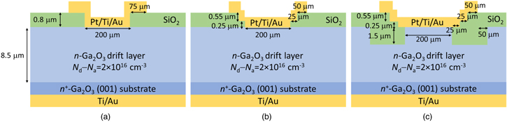
Fig. 1. (Color online) Cross-sectional schematics of Ga2O3 (a) CFP-SBD, (b) SFP-SBD, and (c) TSFP-SBD structures used for TCAD simulation.
Download figure:
Standard image High-resolution imageSimulated electric field profiles of the CFP-SBD, SFP-SBD, and TSFP-SBD operating at a reverse voltage (Vr) of 2 kV are shown in Figs. 2(a)–2(c), respectively. Peak electric fields in the Ga2O3 drift layer and the SiO2 layer under the field plate of the CFP-SBD were estimated to be 5.5 and 12.9 MV cm−1, respectively [Fig. 2(a)]. The peak value in the SiO2 layer exceeds its theoretical breakdown electric field of about 10 MV cm−1, 22,23) that is, the CFP-SBD cannot withstand the Vr of 2 kV. Note that an increase in the thickness of SiO2 is expected to reduce the electric field in it; however, it also increases the electric field in the Ga2O3 region close to the anode edge. The electric field profile of the SFP-SBD shown in Fig. 2(b) provides peak electric fields of 4.6 and 12.8 MV cm−1 in the Ga2O3 and SiO2 layers, respectively. The staircase field plate reduced the peak electric field in the Ga2O3 by about 1 MV cm−1, while that in the SiO2 remained almost the same. The TSFP-SBD had a thick SiO2 region under the field plate, which filled an etched trench as shown in Fig. 1(c). Peak electric fields in the Ga2O3 and SiO2 layers of the TSFP-SBD were estimated to be 4.5 and 10.0 MV cm−1 at Vr = 2 kV, respectively [Fig. 2(c)]; both satisfy requirements for the 2 kV operation. It can also be expected from the simulation that an increase in SiO2 thickness leads to decreasing the peak electric field in it, resulting in further enhancement of Vbr.

Fig. 2. (Color online) Simulated electric field distributions in (a) CFP-SBD, (b) SFP-SBD, and (c) TSFP-SBD at Vr = 2 kV. Portions of the peak electric field in Ga2O3 and SiO2 layers are pointed by white dashed and solid arrows, respectively.
Download figure:
Standard image High-resolution imageBased on the simulation results, we fabricated three types of vertical Ga2O3 SBDs, which had much the same structures as those for the simulations shown in Figs. 1(a)–1(c). A 13 μm thick Si-doped n-Ga2O3 drift layer was grown on an n+-Ga2O3 (001) substrate by halide vapor phase epitaxy (HVPE). 24–26) Note that all the SBDs were simultaneously fabricated on the same epitaxial substrate. The net donor concentration (Nd−Na) of the drift layer was experimentally estimated to be 2 × 1016 cm−3 from capacitance–voltage characteristics. Device fabrication began with the activation of the doped Si donors in the HVPE-grown drift layer by thermal annealing at 1150 °C for 1 hour in N2 ambient. Then, chemical mechanical polishing (CMP) was performed on both sides of the epitaxial substrate to remove damaged regions formed during the substrate production, the HVPE growth, and the activation annealing process as well as to smooth the epilayer surface. After the CMP, the thickness of the n-Ga2O3 drift layer became about 9 μm. Next, 1.5 μm deep trenches were formed on the n-Ga2O3 drift layer by inductively coupled plasma reactive ion etching (RIE) using BCl3. The samples were subsequently annealed in an infrared furnace at 1100 °C for 30 min in N2 to recover the etching damage. It has been observed that high-temperature annealing causes surface charge depletion of the n-Ga2O3 drift layer. 27–30) To remove the depleted region, we performed 400 nm deep etching of the drift layer by BCl3 RIE and CMP after the annealing. Details of the removal process were given in our previous report. 14) Next, 100 nm deep BCl3 RIE was carried out on the substrate back surface to remove a damaged region generated during the previous device processing, and a cathode ohmic electrode was formed on it by blanket evaporation of Ti(20 nm)/Au(280 nm) metal stack and subsequent annealing at 470 °C. Then, a 5 μm thick SiO2 was deposited on the front surface by plasma-enhanced chemical vapor deposition (PECVD) using tetraethoxysilane as shown in Fig. 3(a). Planarization process steps are schematically illustrated in Figs. 3(b)–3(d). First, the trench portions were masked with a photoresist (PR), and a 1.5 μm thick SiO2 was removed by CF4 RIE [Figs. 3(b) and 3(c)]. After removal of the PR mask, CMP was done for planarizing the SiO2 surface and thinning it down to a target thickness of 0.8 μm [Fig. 3(d)]. For fabrication of the CFP-SBDs, the SiO2 was etched using buffered hydrofluoric (BHF) acid solution. The SiO2 steps of the SFP-SBDs and the TSFP-SBDs were defined by CF4 RIE and BHF wet etching. Finally, 200 μm diameter anode electrodes consisted of a Pt(15 nm)/Ti(15 nm)/Au(650 nm) metal stack were fabricated by evaporation and lift-off.
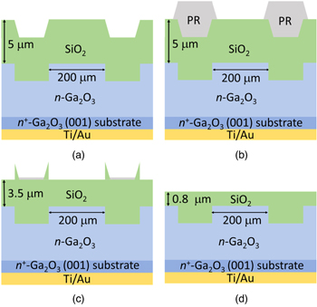
Fig. 3. (Color online) Cross-sectional schematics showing planarization process steps: (a) PECVD SiO2 deposition, (b) trench masking using PR, (c) CF4 RIE of SiO2, and (d) CMP planarization.
Download figure:
Standard image High-resolution imageDC forward current density–voltage (J–V) characteristics of typical Ga2O3 SBDs are shown in Figs. 4(a) and 4(b) in linear and semilogarithmic scales, respectively. Note that both forward and reverse J were normalized by an area of the anode electrode. The turn-on voltage (Von) and Ron of the CFP-SBD, SFP-SBD, and TSFP-SBD were 1.9 V and 4.7 mΩ cm2, 1.9 V and 7.0 mΩ cm2, and 2.1 V and 7.6 mΩ cm2, respectively. The ideality factors of the CFP-SBD, SFP-SBD and TSFP-SBD were 1.41, 1.17 and 1.21, respectively. The relatively large Von and poor ideality factors were attributed to partial removal of the top depletion region formed during the high-temperature annealing; the removal process of the depleted region formed by thermal annealing has to be further improved and/or optimized. Figure 5 shows reverse J–V characteristics of the SBDs. The off-state Vbr of the CFP-SBD, SFP-SBD, and TSFP-SBD were 980, 1530, and 1660 V, respectively. The trend of Vbr validates the TCAD simulation findings on the electric field distribution during the off-state device operation. Figure 6 shows a comparison of Ron–Vbr performance of the TSFP-SBD with those of representative vertical β-Ga2O3 SBDs reported so far. 7–18) It can be considered from the comparison that the TSFP-SBD is as good as state-of-the-art vertical Ga2O3 SBDs in regard to the basic device performance. From these characteristics, the TSFP-SBD structure establishes it as a promising architecture for Ga2O3 SBDs.
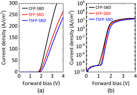
Fig. 4. (Color online) Forward J–V characteristics of Ga2O3 CFP-SBD, SFP-SBD, and TSFP-SBD in (a) linear and (b) semilogarithmic scales.
Download figure:
Standard image High-resolution image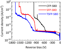
Fig. 5. (Color online) Reverse J–V characteristics of Ga2O3 CFP-SBD, SFP-SBD, and TSFP-SBD.
Download figure:
Standard image High-resolution image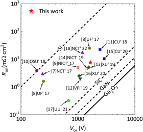
Fig. 6. (Color online) Ron–Vbr benchmark plot of Ga2O3 TSFP-SBD and state-of-the-art vertical Ga2O3 SBDs.
Download figure:
Standard image High-resolution image
In this study, we developed a novel edge termination structure of TSFP, which can contribute to a reduction in peak electric field at both edges of an anode electrode and a field plate. The Ga2O3 TSFP-SBDs exhibited superior device characteristics typified by Ron = 7.6 mΩ cm2 and Vbr = 1.66 kV. This work offered significance of the TSFP structure to enhance Vbr of vertical Ga2O3 SBDs.
Acknowledgments
This work was supported in part by Ministry of Internal Affairs and Communications (MIC) research and development (JPMI00316).