
Abstract
Developing semiconducting solution-processed ultra-wide bandgap amorphous oxide semiconductor is an emerging area of research interest. However, obtaining electrical conduction on it is quite challenging. Here, we demonstrate the insulator-to-semiconductor conversion of solution-processed a-Ga2Ox (Eg ∼ 4.8 eV) through hydrogen annealing. The successful conversion was reflected by the switching thin-film transistor with saturation mobility of 10−2 cm2 V−1s−1. We showed that H incorporated after hydrogen annealing acts as a shallow donor which increased the carrier concentration and shifted the Fermi level (EF) closer to the conduction band minimum.
Export citation and abstract BibTeX RIS
In the current decade, oxide thin-film transistors (TFTs) are evaluated as a strong candidate for Internet of Things (IoT) applications due to excellent uniformity, low threshold voltage, experiment simplicity, low-temperature processability, cost-effectiveness, and compatibility with solution process. 1,2) The next generation IoT industry unceasingly demands new innovations of material exploration and engineering. Developing solution-processed ultra-wide bandgap amorphous oxide semiconductors (UWB-AOSs) is another area of advanced research interest from a materials engineer's perspective. In addition, new UWB-AOSs widen the range of oxide materials applications from industry perspectives. However, obtaining electron conduction in a UWB amorphous material is quite challenging. Therefore, insulator-to-semiconductor conversion of UWB-AOS is among the most fascinating phenomenon to study in materials science and engineering. In this paper, we present insulator-to-semiconductor conversion of solution-processed UWB amorphous gallium oxide (Eg ∼ 4.8 eV).
Amorphous gallium oxide (a-Ga2Ox ) is emerging as a fascinating candidate for solar-blind ultraviolet photodetectors, sensors, and TFTs due to its UWB, high breakdown voltage, high transparency, excellent uniformity, and flexibility on device design. It has decent performance which is comparable with crystalline gallium oxide. 3,4) Other than that, a-Ga2Ox is cost-effective compared to crystalline (c-Ga2O3) or polycrystalline gallium oxide (poly-Ga2O3). Nevertheless, a-Ga2Ox -based TFTs show poor mobility due to their low carrier concentration. For instance, as-deposited a-Ga2Ox is an electrical insulator because the combination of UWB and an amorphous structure has serious difficulties in attaining electronic conduction. In UWB-AOS, a higher doping density is also required to enhance the carrier density. 5) Hence, semiconductor behavior has been hard to achieve. In addition, relatively high impurities during solution-processed deposition contribute to the challenge of realizing semiconductor behavior. There are also only a few researches on solution-processed a-Ga2Ox TFTs, and most studies employ crystalline Ga2O3. These reasons make it much more interesting to conduct this study.
Several research approaches have been proposed in an insulator-to-semiconductor conversion such as deep ultraviolet (DUV) irradiation, flash lamp irradiation, high-temperature annealing, and controlling oxygen partial pressure as well as increasing the film density. 6–9) Mostly, the previous studies focused on vacuum deposition techniques since it forms unquestionably high-quality films as well as high-performance oxide TFTs. Nonetheless, its application is limited because of high cost, high energy requirement, experiment complexity, and difficulty in scaling to large-area electronics. 10,11) Therefore, solution process has become an excellent alternative method due to large-area fabrication, equipment simplicity, atmospheric processing, and low cost. 11) In terms of conversion method, photo-assisted processing such as a flash lamp, excimer laser, and ultraviolet irradiation have been widely used to enhance the electronic properties of wide bandgap (WB) oxide materials (Eg ∼ 3 eV). 7,10,12,13) Nevertheless, the light energy is limited in its application to WB oxide materials since it has insufficient energy to enhance UWB materials (Eg ≥ 4 eV). Moreover, conventional annealing needs to be applied at high temperatures of > 500 °C, which further brings a new issue. It tends to transform oxide materials from an amorphous phase to a crystalline phase which increases the surface roughness that further deteriorates the device performance. 14) Therefore, different approaches to perform the conversion by maintaining its amorphous phase need to be explored.
Herein, we performed hydrogen annealing to obtain semiconducting solution-processed UWB a-Ga2Ox . The key strategy of UWB materials conversion is to increase the carrier concentration, for instance through the bandgap engineering approach. Bandgap engineering is introducing a doping carrier that creates donor states and greatly enhances the electrical properties of n-type semiconductors. It can be performed by incorporating hydrogen through hydrogen annealing. In terms of atomic size, a hydrogen atom is relatively small which likely helped in retaining the gallium oxide film density as well as its amorphous phase. In terms of atomic interaction, hydrogen has multiple roles such as passivation, shallow donor, and defect creation. Hydrogen can act as passivation by passivating the deep state (defect sites due to oxygen deficiency) and interface trap state which reduces the threshold voltage (Vth). It is also well known to be a shallow donor which increases the carrier concentration as hydrogen concentration increases while further enhancing the mobility (μ). However, excessive amounts of hydrogen tend to create interstitial defects which further degrade the device characteristics and cause instability. 15–17) In this work, we have successfully obtained semiconducting solution-processed a-Ga2Ox -TFTs which was demonstrated by the switching TFT behavior with saturation mobility (μsat) of 10−2 cm2 V−1s−1.
A gallium oxide precursor (0.5 M) was synthesized by dissolving gallium nitrate hydrate (Ga(NO3)3
 H2O 99.999%, Sigma-Aldrich) in 2-methoxyethanol (C3H8O2 anhydrous 99.8%, Sigma-Aldrich) under constant stirring at room temperature for 12 h. The a-Ga2Ox
channel was deposited via a spin coating technique at 2000 rpm for 15 s followed by a two-step baking process. The multiple-step baking process was subsequently performed until an ∼80 nm thick a-Ga2Ox
film was formed. The baking temperatures were determined by Thermogravimetry/Differential Thermal Analysis (TG-DTA; Hitachi DSC7000) curves of a-Ga2Ox
precursor. Moreover, the a-Ga2Ox
film was annealed at 500 °C for 2 h under various gases (N2:O2 80:20%, 100% N2, and H2:N2 96:4%,) which continuously flowed at a flow rate of 500 sccm. Finally, a-Ga2Ox
channel-islands were patterned by standard photolithography followed by 100 nm aluminum metal deposition via electron beam evaporation as a source and drain. Bottom-gate top-contact a-Ga2Ox
TFTs were fabricated on a p-type Si gate electrode with 85 nm thermally oxidized SiO2 layer as the gate insulator. It should be noted that there was no additional post-metallization annealing performed after metal electrode deposition. The electrical characteristics of a-Ga2Ox
TFT were analyzed using a semiconductor parameter analyzer (Agilent Technologies B1500A). Film thickness, phase structure, and film density were characterized and determined by a profilometer, grazing incidence X-ray diffraction (XRD; Rigaku SmartLab9kW/IP/HY/N), and X-ray reflectivity spectroscopy (XRR; Rigaku SmartLab9kW/IP/HY/N), respectively. Optical bandgap values (Eg) and valence band offset (EV-offset) were estimated by ultraviolet–visible spectroscopy (UV–vis; JASCO ILN-472) Tauc plot and X-ray photoemission spectroscopy (XPS; ULVAC-PHI 5000 VersaProbell). Finally, elemental analysis and hydrogen diffusion were evaluated by secondary ion mass spectroscopy (SIMS; ULVAC-PHI ADEPT-1010).
H2O 99.999%, Sigma-Aldrich) in 2-methoxyethanol (C3H8O2 anhydrous 99.8%, Sigma-Aldrich) under constant stirring at room temperature for 12 h. The a-Ga2Ox
channel was deposited via a spin coating technique at 2000 rpm for 15 s followed by a two-step baking process. The multiple-step baking process was subsequently performed until an ∼80 nm thick a-Ga2Ox
film was formed. The baking temperatures were determined by Thermogravimetry/Differential Thermal Analysis (TG-DTA; Hitachi DSC7000) curves of a-Ga2Ox
precursor. Moreover, the a-Ga2Ox
film was annealed at 500 °C for 2 h under various gases (N2:O2 80:20%, 100% N2, and H2:N2 96:4%,) which continuously flowed at a flow rate of 500 sccm. Finally, a-Ga2Ox
channel-islands were patterned by standard photolithography followed by 100 nm aluminum metal deposition via electron beam evaporation as a source and drain. Bottom-gate top-contact a-Ga2Ox
TFTs were fabricated on a p-type Si gate electrode with 85 nm thermally oxidized SiO2 layer as the gate insulator. It should be noted that there was no additional post-metallization annealing performed after metal electrode deposition. The electrical characteristics of a-Ga2Ox
TFT were analyzed using a semiconductor parameter analyzer (Agilent Technologies B1500A). Film thickness, phase structure, and film density were characterized and determined by a profilometer, grazing incidence X-ray diffraction (XRD; Rigaku SmartLab9kW/IP/HY/N), and X-ray reflectivity spectroscopy (XRR; Rigaku SmartLab9kW/IP/HY/N), respectively. Optical bandgap values (Eg) and valence band offset (EV-offset) were estimated by ultraviolet–visible spectroscopy (UV–vis; JASCO ILN-472) Tauc plot and X-ray photoemission spectroscopy (XPS; ULVAC-PHI 5000 VersaProbell). Finally, elemental analysis and hydrogen diffusion were evaluated by secondary ion mass spectroscopy (SIMS; ULVAC-PHI ADEPT-1010).
In fabricating a-Ga2Ox film via solution process, temperature selection for pre-baking and post-baking are vital considerations since these temperatures can control the channel's film quality. The pre-baking and post-baking temperatures were determined by analyzing the thermal properties of a-Ga2Ox precursor through TG-DTA measurement as shown in Fig. S1(a) (available online at stacks.iop.org/APEX/15/024003/mmedia) in the supplementary section. The Ga2Ox precursor solution exhibited gradual mass loss from ∼25 °C to 120 °C which indicates evaporation of the solvent. The 2-methoxyethanol was completely evaporated when it reaches the boiling point at 124 °C which is also indicated by the ∼90% mass loss. The hydrate compound was removed via thermally driven hydrolysis at ∼100 °C indicated by a deep peak of endothermic reaction in the DTA curve. While the nitrate compound was removed via thermal decomposition at 124 °C to 138 °C which was observed as ∼4% weight loss. Hence the pre-bake temperature was chosen at 150 °C to ensure that the solvent and precursor-related impurities have been completely removed. The metal oxide started to form at ∼200 °C and was followed by densification at 380 °C. While the film was crystallized at 680 °C. Hence the post-bake temperature was chosen at 500 °C to ensure the metal oxide formation and densification of the film without changing its phase to crystalline. By applying both pre-bake and post-bake temperatures, we expect that an as-deposited a-Ga2Ox film will be formed.
The as-deposited a-Ga2Ox films were further annealed inside a quartz chamber at 500 °C under a certain gas environment. Several gases (N2, H2, and O2) continuously flowed at 500 sccm for 2 h as illustrated in Fig. S1(b). After varying the annealing environment, the annealed films were patterned and followed by metal electrode deposition [Fig. S1(c)]. Finally, the a-Ga2Ox TFT characteristics were evaluated and shown in Fig. 1, while the TFT performance is summarized in Table I.
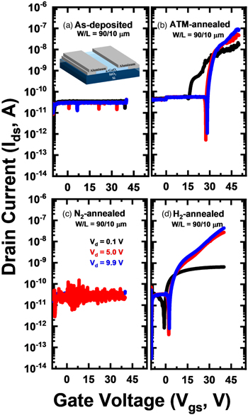
Fig. 1. (Color online) TFT transfer curves of (a) as-deposited, (b) ATM-annealed, (c) N2-annealed, and (d) H2-annealed of Ga2Ox film.
Download figure:
Standard image High-resolution imageTable I. Summary of Ga2Ox TFT performance under different annealing ambient.
| Annealing ambient | Gases | μsat (cm2 V−1s−1) | Vth (V) | SS (V dec−1) | ON/OFF ratio |
|---|---|---|---|---|---|
| As-deposited | No annealing | No switching | |||
| ATM-annealed | N2:O2 (80:20%) | (7.6 ± 0.9) × 10−2 | 13.0 ± 2.8 | 0.16 ± 0.07 | ∼104 |
| H2-annealed | N2:H2 (96:4%) | (1.0 ± 0.01) × 10−2 | 1.7 ± 0.2 | 0.34 ± 0.20 | ∼104 |
| N2-annealed | N2 (100%) | No switching | |||
The measured a-Ga2Ox
TFTs had a channel width and length (W/L) of 90/10 μm. The electrical characteristics such as μsat, threshold voltage (Vth) and subthreshold swing (SS) during saturation mode (Vds = 5 V) were obtained based on the approximate equation for TFT in saturation mode:  where μ obtained from the equation:
 is the drain current,
  is the gate insulator capacitance,
  is the gate voltage,
  is the drain voltage, and
  is the transconductance.
The as-deposited a-Ga2Ox TFT is completely inactive because of its insufficient carrier concentration, UWB, and amorphous phase. Due to those complex combinations, a-Ga2Ox tends to retain its insulating state. Therefore, semiconducting a-Ga2Ox has been hard to obtain. As expected, the annealed samples showed device improvement. To further study the cause of this improvement, a different gas environment flowed during annealing while maintaining the temperature at 500 °C. This experiment was performed to separate the effect of annealing temperature and annealing ambient (gases).
As we can observe in Fig. 1, the switching behavior was obtained for atmosphere-annealed (ATM-annealed) and H2-annealed samples. While the N2-annealed samples show problematic switching. In order to elucidate the switching behavior, film characterization such as XRR, XRD and UV–vis were performed and the results are summarized in Fig. 2 and Table II.
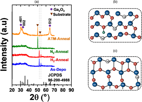
Fig. 2. (Color online) (a) XRD spectra of Ga2Ox film. Phase change illustration of (b) a-Ga2Ox into (c) poly-Ga2Ox .
Download figure:
Standard image High-resolution imageTable II. Physical and optical properties of Ga2Ox film under different annealing ambient.
| Annealing ambient | Thickness (nm) | Roughness (nm) | Film density (g cm−3) | Phase structure | Eu (meV) | Eg (eV) |
|---|---|---|---|---|---|---|
| As-deposited | 20.6 | 0.47 | 4.14 | a-Ga2Ox | 362.2 | 4.80 |
| ATM-annealed | 20.7 | 0.70 | 5.13 | poly-Ga2O3 | 468.1 | 4.66 |
| H2-annealed | 21.0 | 0.45 | 4.11 | a-Ga2Ox | 746.9 | 4.22 |
| N2-annealed | 22.0 | 0.50 | 4.17 | a-Ga2Ox | 388.1 | 4.60 |
The diffraction spectra in Fig. 2(a) clarified that most films were amorphous, except for the ATM-annealed film. It obviously separated the effect of annealing temperature and annealing ambient. By only annealing the film at 500 °C, the crystallized film will generally not be obtained. Moreover, the film crystallization is apparently dependent on the annealing ambient. In the ATM-annealed film, certain peaks of monoclinic c-Ga2O3 were observed which indicates that the film has started to crystallize. As impurities evaporated during annealing, the Ga–O bond was rearranged and transformed its amorphous structure [Fig. 2(b)] into crystalline-like structure [Fig. 2(c)].
The O2 gas apparently takes an important role in film crystallization since it leads to Ga–O bond rearrangement at certain temperatures. Hence, ATM annealing ambient significantly modified the Ga2Ox phase structure despite being annealed under the crystallization temperature (680 °C) suggested by TG-DTA, resulting in poly-Ga2O3. On the other hand, the films treated under N2 and H2 ambient remained the same as an amorphous structure which emphasizes that both gases (N2 and H2) did not induce Ga2Ox film crystallization. Therefore, switching the TFT of the ATM-annealed [Fig. 1(b)] sample was due to film crystallization. Furthermore, as the film was crystallized, the film density increased to 5.13 g cm−3. A film density of ∼5.2 g cm−3 is expected in semiconducting a-Ga2Ox film. 8) However, poly-Ga2O3 has higher surface roughness which induces interfacial traps, resulting in inferior device performance. 18) Likewise, the charge trapping of n-type semiconductors at the interface tends to shift the Vth positively. In addition, some noise is observed in the transfer curve [Fig. 1(b)] which likely indicates a poor channel-gate insulator interface roughness.
In the case of N2 and H2-annealing, both films retained an amorphous structure, similar film density, and as well as surface roughness. However, interestingly adding 4% H2 gas can significantly improve the conductivity which is reflected by switching TFT [Fig. 1(d)]. In addition, the ON curve was successfully obtained at extremely lower drain voltage (Vd) ≤ 9.9 V, unlike other reported a-Ga2Ox TFTs which require higher Vd up to 50 V. 8,19,20) Nevertheless, the 100% N2 annealing did not show switching behavior which emphasizes that both annealing temperature (500 °C) and N2 gas were insufficient to enhance the a-Ga2Ox . Therefore, switching TFT of H2 and ATM-annealed were reflected as the success of insulator-to-semiconductor conversion. Considering the relatively lower film density of solution-processed semiconducting a-Ga2Ox (4.11 g cm−3) compared to its vacuum-processed counterpart (5.20 g cm−3), 8) it is still possible to enhance the TFT performance by increasing the film density. We summarized the reported film density of solution-processed and vacuum-processed gallium oxide in Table SI in the supplementary section. The solution-deposited film has a relatively ∼ 1 g cm−3 lower film density than vacuum-deposited film. One method to improve the film density while retaining its amorphous phase is through doping. Depending on the dopant, the film density can be increased up to ∼4.8 g cm−3. Nevertheless, semiconducting UWB a-Ga2Ox which was obtained from H2-annealing needs to be understood since it retained its amorphous structure even after annealing.
To further elucidate the switching of the H2-annealed sample, optical properties, as well as the band diagram alignment, were evaluated. The optical properties such as optical bandgap (Eg), Fermi level (EF) and Urbach energy (Eu) of each film were calculated from the UV–vis and XPS spectra. The optical bandgap was obtained through the Tauc equation:  for direct bandgap, where
  is the absorption coefficient, A is the constant slope parameter,
  is photon energy, and
  is the bandgap energy. While the Fermi level (
 ) relative position was obtained by subtracting the Eg and valence band offset (
 ). The Urbach energy (Eu) was obtained from the Urbach relation
The optical property was represented as the Eu and Eg in Table II, where both energies were shifted as different annealing ambient were applied. The Eu is a combination of both conduction band (CB) and valence band (VB) tail states. It indicates the subgap disorder level of oxide materials which might have originated from low/poor crystallinity, amorphous disorder, and defect impurity. Wider optical absorption indicates higher subgap disorder as displayed in Fig. 3(a). The film disorder tends to increase after annealing. The ATM-annealed film has just started to crystallize, forming poly-Ga2O3 amidst an amorphous structure and resulting relatively high subgap disorder of Eu = 468.1 meV. This assumption that the ATM-annealed film has started to crystallize is supported by its high film density (5.13 g cm−3) which is relatively lower compared to the majority of c-Ga2O3 (5.30–6.30 g cm−3) 21,22) and higher compared to the other samples (4.11–4.17 g cm−3). The subgap disorder of N2-annealed film might have originated from the amorphous disorder with a relatively lower Eu of 388.1 meV. Furthermore, the H2-annealed film has the highest subgap disorder (Eu = 746.9 meV) due to a combination of amorphous disorder and hydrogen defect impurity. Those defects tend to create tail states in the bandgap edges. In AOS such as a-IGZO and a-Ga2Ox , the energy width of VB tail states is larger than CB tail states, implying that the Eu better represents the VB tail states. 1,9) Hence, additional acceptor states were created above the valence band maximum (VBM). However, the H2 gas serves as a shallow donor which increased the carrier concentration and is reflected as a switching TFT. Therefore, additional donor states were created specifically for the H2-annealed samples [Fig. 3(d)].

Fig. 3. (Color online) (a) Optical absorption, (b) XPS, (c) SIMS and (d) band diagram alignment of Ga2Ox in different annealing ambient.
Download figure:
Standard image High-resolution image
Hereinafter, the Eg was also shifted from 4.80 to 4.22 eV as different annealing ambient were applied. The Eg shifting might be caused by annealing, doping introduction or change of carrier concentration. 23,24) In the case of ATM and N2 annealing, the Eg shifted from 4.80 to 4.66 and 4.60 eV, respectively. Interestingly, as 4% H2 gas was introduced, the Eg shifted even lower up to 4.22 eV [Fig. 3(d)]. This is due to the H2 doping introduction. The H2 gas which continuously flowed was diffused and incorporated into a-Ga2Ox bulk film, which further increased the carrier concentration. The increase in carrier concentration successfully enhanced the a-Ga2Ox film into a semiconductor which is reflected by the switching TFT. Furthermore, it created additional donor states which further shifted EF closer to the conduction band minimum (CBM) [Fig. 3(d)]. In addition, Hall measurement was performed to estimate the carrier density of the H2-annealed sample. It was observed that the carrier density of as-deposited and H2-annealed were estimated as 1 × 10¹⁰ (1 cm−3) and 6 × 10¹¹ (1 cm−3), respectively, which represent a 1 order increase in magnitude after H2-annealing.
To support our hypothesis, XPS and SIMS were conducted to further investigate the H-incorporation. All XPS spectra were calibrated with the Ga2p peak at 1118.0 eV. The O1s spectra were fitted with three peaks and the FWHM was fixed at 1.4 ± 0.1 eV. The peak centered at 530.6 ± 0.1 eV can be assigned to oxygen in gallium oxide lattice (Ga–O). The peak exhibited at 531.2 ± 0.1 eV is related to the gallium oxide lattice with an oxygen vacancy (Ga–Vo), whereas the peak at 532.1 ± 0.1 eV arises from hydroxide-related bonds (Ga–OH). 25) The deconvoluted peaks were summarized in Fig. 3(b). The as-deposited film shows a low Ga–O bond which suggests either fewer Ga–O bonds or several Ga–O are loosely bound [Fig. S2(a)]. Once the annealing treatment was applied, the Ga–O bonds were reorganized and reinforced which is reflected in the higher percentage of Ga–O after annealing. The thermally driven band rearrangement was also reflected in the amount of oxygen vacancies in each film as well as the hydroxide-related peaks (Fig. S2(b)]. The Ga–OH percentage was gradually decreased for H2-annealed, ATM-annealed and N2-annealed, respectively. A similar trend was also observed in the SIMS spectrum. Those Ga–OH might indicate either H-impurities or H-incorporated. The H-impurity originated from the precursor or H2O environment impurity (relative humidity) which might be attached to the film during solution deposition. While the H-incorporated refers to the H2 gas which were incorporated into the film during H2 annealing. However, it is quite difficult to distinguish which H was contributed more. Therefore, the following mechanism was proposed to elaborate the H-incorporation phenomena as illustrated in Fig. S2(c).
Figure S2(c) illustrates that the as-deposited film has relatively high H-impurities. Excessively high amounts of H-impurities create interstitial defects which further deteriorate the device performance. 17) It was reflected by the non-switching of the as-deposited a-Ga2Ox TFT. As annealing was applied, the impurities were evaporated which was indicated by the ∼10% decrease of Ga-OH percentage area (N2-annealed sample). Simultaneously, as 4% H2 gas was introduced, the Ga-OH percentage area was increased by ∼5% (H2-annealed sample). It emphasizes that the H2 gas which flowed during annealing was diffused and incorporated into the a-Ga2Ox film which further serves as a shallow donor. At certain amounts, H acts as a shallow donor which is reflected in the switching of the H2-annealed a-Ga2Ox TFT. The H2 gas (H+ atom) binds to oxygen creating O–H bond and serves as a shallow donor in a-Ga2Ox . 26) However, excessive H tends to create interstitial defects, while lower H might refer to insufficient carrier concentration. Therefore, controlling the H percentage is crucial. In addition, it is possible that the un-annealed (as-deposited) a-Ga2Ox has a relatively high electron trap density due to poor film quality. The film quality was improved after H2-annealing since hydrogen passivated the electron trap states and induced semiconducting behavior. Furthermore, we expect that this conversion will likely remain stable. 27) Nevertheless, it is also possible that the H2-annealed a-Ga2Ox exhibits thermal instability. Therefore, the thermal stability of H2-annealed a-Ga2Ox needs to be further investigated.
In summary, we have demonstrated that solution-processed a-Ga2Ox (Eg > 4.8 eV) insulator can be converted into a semiconductor which is reflected by the TFT switching behavior. We found that performing H2 annealing at 500 °C induced hydrogen incorporation which further serves as a shallow donor in insulating a-Ga2Ox . The hydrogen incorporation leads to an increase in electron carrier concentration as reflected by EF shifting closer to the CBM. H2 annealing is a promising method that can be used to enhance other ultra-wide bandgap oxide materials.
Acknowledgments
The authors would like to acknowledge NAIST Grant-in-Aid and NAIST Data Science Grant for supporting this work.