

Abstract
The past several decades have witnessed a vast array of developments in printable organic semiconductors, where successes both in synthetic chemistry and in printing technology constituted a key step forward to the realization of printed electronics. In this Review, we highlight specifically materials science, charge transport, and device engineering of—two-dimensional single crystals—. Defect-free organic single-crystalline wafers manufactured via a one-shot printing process allow remarkably reliable implementations of organic thin-film transistors with decently high carrier mobility up to 10 cm2 V−1 s−1, which has revolutionized the current printing electronics to be able to meet looming internet of things challenges. This Review focuses on the perspective of printing two-dimensional single crystals with reasonable areal coverage, showing their promising applications for practical devices and future human society, particularly based on our recent contributions.
Export citation and abstract BibTeX RIS
1. Introduction
"Internet-of-Things" (IoT), firstly termed by Kevin Ashton in 1999, has attracted growing attention as the key technology for the next-generation society, in which a variety of things are monitored and networked. As an enormous number of sensors are indispensable for monitoring, the realization of Trillion Sensors Universe has been proposed. As well, communication tools such as radio-frequency identification (RFID) tags are required. Hence, technological innovations for low-cost and mass-producible high-end electronic devices are of current interest. Particularly, an approach to the low-cost device is the employment of components that are low-cost per unit area. In today's information-oriented society, silicon wafer-based metal-oxide-semiconductor field-effect transistors (MOSFETs) are indispensable elements for integrated logic circuits. In MOSFETs, the on-off switching function is given only within a few nanometers at the outermost surface of the sub-millimeter-thick wafers, thus the materials utilization efficiency is not high. By contrast, two-dimensional (2D) materials, such as graphene and transition metal dichalcogenides, are the potential alternatives of silicon due to their atomically thin natures and high carrier mobilities, whereas they leave the crucial tasks of scalability or mass producibility. As such, semiconducting materials exhibiting the 2D sheet-like, the thin-film structural feature can be great candidates for low-cost devices as well as low materials consumption. Organic semiconductors are representative of such materials and thus have been extensively investigated from the viewpoints of materials chemistry, physics, and engineering. Although early major works on thin-film transistors based on organic semiconductors, namely, organic thin-film transistors (OTFTs), were developed with vacuum evaporated thin films, 1,2) solution processes are the current key technology for printed electronics. Solution techniques, such as spin-coating and dip-coating methods, have been conventionally used for forming amorphous or polycrystalline thin films. However, sophisticated solution techniques have made recent progress in printing single-crystal thin films of organic semiconductors in a large area owing to the self-assembly properties of molecular materials. Those single crystals can be grown in a sheet-like shape with the thickness of a few nanometers (corresponding to one-to-several molecular thickness), where a charge transport layer can be confined in the few-nanometer-thick 2D space composed of π-conjugated molecules (vide infra). 3) Hence, the emergence of printed single crystals leads organic semiconductors to actual 2D materials. In addition to the printable feature at moderate temperatures, the single crystal is suitable for OTFT applications due to its long-range ordered structures with negligible defects and grain boundaries, leading to high charge carrier mobilities. That is, the 2D organic semiconductor single crystals, which are printable at moderate temperatures, promise low materials consumption and exhibit excellent electronic properties, are the promising class of materials for high-end electronic devices. Therefore, further developments of fabrication and application abilities are demanded at this stage.
In this Review, the topic will be focused on the emerging technology of scalable fabrication of 2D organic semiconductor single crystals by solution techniques and their use for high-performance OTFTs (Fig. 1). We first note the chemical characteristics of organic semiconductors and their aggregated structures in the solid states. In the following sections, solution techniques for 2D single crystals are introduced, starting from the early contributions to the latest achievements.
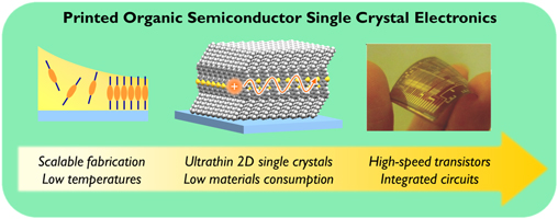
Fig. 1. (Color online) Perspectives of printed organic semiconductor single crystals for electronics applications. Reprinted with permission from Ref. 68 Copyright 2017 Wiley-VCH GmbH.
Download figure:
Standard image High-resolution image2. Organic semiconductors and 2D single crystals
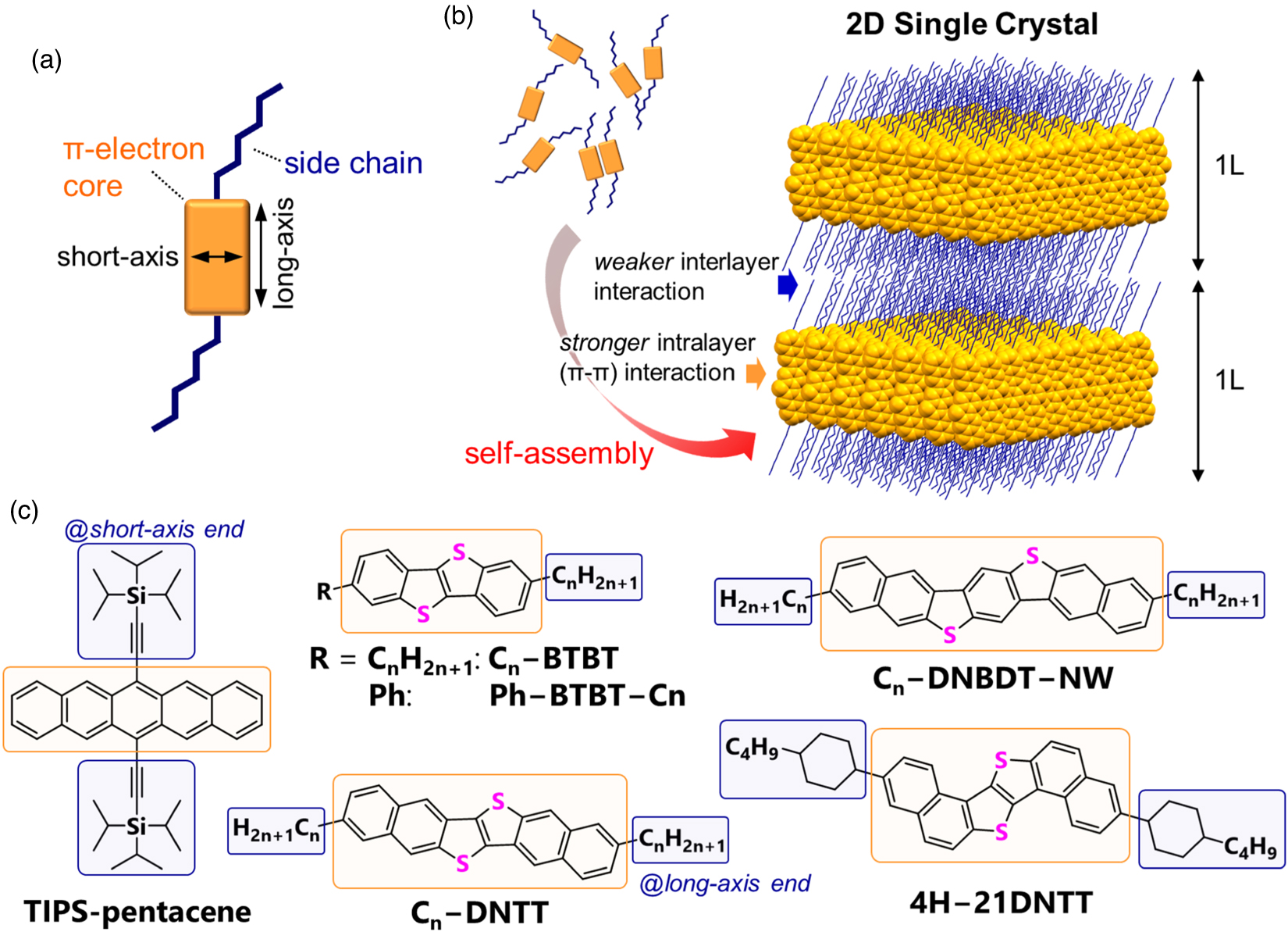
Organic semiconductors are the aggregated solids of π-conjugated (organic) molecules. When the π-electron cores are closely packed in a long-range with effective π–π interactions, the pathway of charge carriers is formed via the π–π interactions. Compared to traditional organic semiconductor molecules solely composed of a π-electron core, 4,5) recent functional molecules often bear (insulating) side chains attached to the π-electron core, 6) which increases solubility in organic solvents, giving solution processability [Fig. 2(a)]. The molecules are self-assembled in solutions or at solution interfaces to crystallize. During crystallization, the side chains may affect packing structures and morphologies. In addition, 2D layered structures could be stabilized if the chemical properties of side chains and π-electron cores are remarkably different; for example, the representative side chain is aliphatic alkyl groups while the π-electron cores are aromatic [Fig. 2(b)]. Moreover, the interlayer interaction can be weaker than the intralayer interaction mainly governed by π–π interactions particularly in the case of aliphatic alkyl side chains. Considering that a 2D layer is the one-molecular layer (1L) thick, the weak interlayer interactions can lead to less dominant crystal growths along the out-of-layer (thickness) direction compared to the in-layer dimensions. For printing 2D single crystals, molecular structures are important in addition to process conditions to precisely suppress and control the crystal thicknesses, i.e. the number of molecular layers. Representative organic semiconductors applicable for large-area printing processes are shown in Fig. 2(c). 7–12) Briefly, they can be categorized into two systems: rod-like π-electron cores bearing side chains at (1) the short- and (2) the long-axis end, where TIPS-pentacene is the representative of the category (1), while the others shown in Fig. 2(e) belong to category (2). It is noteworthy that bulky groups represented by (trialkylsilyl)ethynyl group are generally employed for materials in category (1), whereas those in category (2) generally bear flexible alkyl groups as the side chain. Due to possible layered assembly of the flexible alkyl chains as demonstrated by self-assembled monolayers, materials in category (2) can be generally suitable for 2D crystal growths through individual 2D assembling capabilities of π-electron cores and alkyl side chains. On the other hand, the bulky side chains with three-way-branched alkyl moieties would lead to easier crystal growths to the out-of-layer directions, which is not preferred for 2D crystals. These different features may affect the processability of organic semiconductors discussed in the following sections.

Fig. 2. (Color online) Organic semiconductors growing 2D single crystals. (a) Schematic model of typical organic semiconductor molecular structure bearing side chains. (b) Schematic illustration of the self-assembled 2D single crystal of organic semiconductors. π-cores and side chains are depicted by space-filling (orange) and stick (blue) models, respectively. (c) Representative organic semiconductors suitable for large-area printing methods. n: the number of carbon atoms in the alkyl group, typically n = 8−12. Orange and blue shadows represent the rod-like π-electron core and side chain moieties, respectively.
Download figure:
Standard image High-resolution image3. Emergence and development of printed organic semiconductor single crystals
Due to the lack of appropriate materials and solution techniques, early studies on single crystal OTFTs were carried out by using thin crystals obtained by the physical vapor transport method. 13–15) Thanks to the progress in syntheses of soluble, high-performance organic semiconductors, the research interest moved into the concept of printing organic semiconductors. Especially for single crystals, in 2009, Uemura and Takeya et al. reported a methodology to realize this concept by controlling the unidirectionally oriented evaporation of the solvent from solutions including organic semiconductor molecules C8-BTBT. 16) This method relies on the use of a solution-sustaining piece [Fig. 3(a)], which makes a meniscus at the substrate-solution-air interface owing to surface tension effects. The meniscus guides crystallizations, i.e. crystallizations occur at the edge of the meniscus; hence, we refer to this printing method as "edge casting." Single crystalline thin films of C8-BTBT were successfully formed on a decyltriethoxysilane-functionalized substrate from the heptane solution [Fig. 3(b)], affording the hole mobilities between 3.5 and 5.0 cm2 V−1 s−1. Henceforward, the concept of edge casting was extended to other organic semiconductors, 17,18) whereas a variety of solution techniques have been shown for 2D single crystals. The attention was paid not only to printing but also to simultaneous patterning; for example, double inkjet printing enabled controlled recrystallization, 19) and a confined space guided by a stamp makes meniscus similarly to edge casting. 20) Besides, various fascinating solution techniques aim at large-area and ultimately thin 2D single crystals. 21) Hu and co-workers have developed facile methods to grow various organic single crystals on the water surface. 22–24) For example, in a methodology named "solution epitaxy," microcrystals were firstly prepared by drying organic semiconductor solutions on the water surface, which were used as the seeds for larger crystals during the subsequent drop-casting process, allowing millimeter-scale single crystals with few molecular thicknesses. 22) Interestingly, the addition of surfactant to the water enabled larger 2D crystal growths in one step due to a change in interfacial tension of the water/solution system. 24) For another case, a gravity-assisted 2D spatial confinement method, where organic semiconductor solution slowly dries up in a confined space sandwiched by two solid substrates, enabled the growth of 1L thick single crystals of specific organic semiconductor material. 25) These 2D single crystals have been successfully applied for OTFTs as the proposed high-performance semiconductor layers. As such, solution-based 2D single crystals of organic semiconductors have gained attention as new materials for electronic devices; therefore, extensive studies have been further carried out to advance them to more practical technologies, such as reproducible and more scalable printing methods.
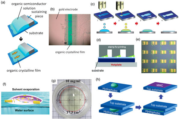
Fig. 3. (Color online) Examples of reported fabrication methods for single-crystal thin films. (a) Edge casting method using a solution-sustaining piece and (b) an optical microscope image of the resultant OTFT. Reprinted with permission from Ref. 16 Copyright 2009 IOP Publishing. (c) Double-inkjet printing. Reprinted with permission from Ref. 19 Copyright 2011 Springer Nature. (d) Patternable crystallization at gap-mediated meniscus and (e) an optical microscope image of the OTFT array. Reprinted with permission from Ref. 20 Copyright 2011 Wiley-VCH GmbH. (f) Schematic image of the solution epitaxy method. Reprinted with permission from Ref. 22 Copyright 2016 Wiley-VCH GmbH. (g) Enhanced solution epitaxy based on the surfactant-controlled water surface. Reprinted with permission from Ref. 24. 2018 American Chemical Society. (h) Growth of thin crystals via evaporation of the solvent in a confined space. Reprinted with permission from Ref. 25 Copyright 2018 Springer Nature.
Download figure:
Standard image High-resolution image4. Meniscus-guided coating method for large-area single crystal-based OTFTs
As shown above, crystal growths at the meniscus region of the substrate-solution interface can provide opportunities for high-performance OTFTs. To apply this advantage to printed electronics, large-scale printing methods, namely, meniscus-guided coating (MGC) methods, have been developed. 26) Hereafter, we would like to move on to the MGC methods for OTFTs, especially based on organic semiconductor single crystals, as the special focus in this Review.
4.1. MGC based on dip-coating technique
In principle, the meniscus is always formed at the edge of the solid−liquid interface. Thus, evaporation of solvent from organic semiconductor solution along a single direction, unlike drop-casting, could afford unidirectionally-orienting or single-crystal organic semiconductor thin films. A simple MGC method to realize such a situation is the dip-coating method. By dip coating, the meniscus is at the three-point contact area among air, solution and substrate, which is formed by pulling up the substrates from a bath of organic semiconductor solution. With small-molecular organic semiconductors, the dip coating has usually afforded thin films with microstripe-like morphologies 27–32) [Figs. 4(a)–4(b)]. Amongst the key factors of the dip coating method, the most easily tunable factors are solvent evaporation rate, solution concentration, solute solubility and pulling speed [Fig. 4(c)], 30) which could lead to monolayer to multilayer thin film formations. Yet, the uncertainty of uniformity and crystallinity have been left as the crucial issue of dip coating of small-molecule organic semiconductors although the dip-coating method implied potential applications for large-area thin-film growths. Note that recent studies on dip coating have shown deeper insights into meniscus shape 32) and usefulness for scalable polycrystalline thin films of Ph-BTBT-C10 and C8-BTBT, 33) giving the prospect of rapid applications for polycrystalline OTFTs.

Fig. 4. (Color online) (a) Schematic illustration of the dip-coating method and (b) dip-coated microstripes of DTBDT-C9. Reprinted with permission from Ref. 27. 2010 American Chemical Society. (c) The key factors in the dip-coating method. Amongst them, solvent evaporation, solution concentration, solute solubility and pulling speed (highlighted by red frames) are easily tuned in the experiments. Reprinted with permission from Ref. 30 Copyright 2016 American Chemical Society.
Download figure:
Standard image High-resolution image4.2. MGC using a solution-sustaining blade
Scalable MGC techniques more suitable for single-crystal organic semiconductor thin films have been developed by using a solution-sustaining plate, conventionally called "blade." In 2008, Bao et al. reported a shearing of organic semiconductor solutions by the blade on the substrates could form a unidirectional meniscus, followed by evaporation of solvent to grow aligned crystalline films on the substrates. 34) This is commonly called the solution-shearing method, which has not only provided the aligned crystals but also forced lattice strain 35) or blade-shape-derived crystallinity enhancement. 36) To date, many efforts have been further devoted to understandings, improvements and applications of MGC methods. 37–43) In particular, aligned and dense crystalline (ultimately, single crystal) thin films can be obtained by using appropriate organic semiconductor materials and optimum processing conditions. One of the recent fascinating studies is the production of large-area single-crystal thin films of Ph-BTBT-Cn. Although the pure Ph-BTBT-Cn could form moderate single-crystal thin films, the MGC of mixed Ph-BTBT-Cn materials with difference alkyl chain lengths (n) can lead to remarkably large-area single-crystal thin films with controlled film thicknesses. 39) In addition, a bar-coating method, where a cylindrical bar is used instead of the plate-shaped blade, would be beneficial because the solutions under the bars are less confined near the contact line and the effects induced by the blade edge can be minimized. 44,45)
4.3. MGC using a blade with continuous solution supply
Although the MGC methods shown in Sect. 4.2 are promising for large-area printing of single-crystal thin films, a practically scalable printing technology (ideally, roll-to-roll technology) should require continuous production of the uniform single-crystal thin films beyond the wafer scale. In such cases, most of the abovementioned MGC methods are not satisfactory because the organic semiconductor solutions can be supplied only in advance of the coating processes, thus limiting the coating area. The continuous solution supply has been traditionally described by the zone-casting method [Figs. 5(a)–5(b)], 37,46–48) whereas zone casting had not afforded large-area single crystals presumably due to the inappropriate meniscus shapes. Thinking conjunction of continuous solution supply with sophisticated meniscus controls by edge casting method, Takeya and co-workers have intensively developed an advanced MGC method, namely, continuous edge casting 49–51) (CEC). The schematic illustration of CEC is shown in Fig. 5(a). To explain briefly, the blade is appropriately away from the substrate to make the organic semiconductor solution, which is supplied from one side [the left side in Fig. 5(c)] of the blade, spread well around in-between the substrate and the blade to form the controlled meniscus. With continuously supplying the solution, the substrate is moved vertically to the face of the blade [i.e. from left to right in Fig. 5(c)]. During these processes, the solvent is evaporated at the three-point contact area in the substrate movement direction [i.e. right side in Fig. 5(c)], leading to the growth of aligned crystalline thin films on the substrate. Owing to solution flow caused by the substrate movement, the crystal growth direction can be aligned to a specific crystallographic direction dependent on the molecular and the crystal structures. Controllable processing parameters are the concentration of the organic semiconductor solution, temperatures of the solution and the substrate, and speed of the solution supply and substrate movement. The first work of CEC reported inch-size single-crystal thin films of C10-DNBDT-NW, where the single-crystal features were confirmed by X-ray diffraction and cross-polarized optical microscopy [Figs. 5(d)–5(e)]. The OTFT characteristics revealed the highest and average hole mobilities of 9.5 and 7.5 cm2 V−1 s−1, respectively, which approached the intrinsic hole mobility of C10-DNBDT-NW 11) of 16 cm2 V−1 s−1 while the lower hole mobilities in OTFTs via CEC were probably due to the uncontrolled thickness and the geometrical factor.
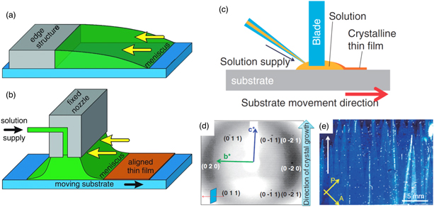
Fig. 5. (Color online) Schematic setup of (a) edge casting and (b) zone casting. Reprinted with permission from Ref. 37 Copyright 2016 Wiley-VCH GmbH. (c) Schematic illustration of continuous edge casting (CEC), and resultant (d) in-plane X-ray diffraction and (e) cross-polarized optical microscope images of C10-DNBDT-NW. Reprinted with permission from Ref. 49 Copyright 2013 IOP Publishing.
Download figure:
Standard image High-resolution image4.4. Control of crystal dimensions for high-performance OTFTs
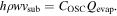
To improve the quality of single-crystal thin films by MGC, the guidelines for optimum processing conditions may principally rely on the evaporation rate of the solvent (Qevap) and the speed of the substrate movement (vsub) (Fig. 6). 52,53) In the case vsub > Qevap, the thickness of coated film would be increased with increasing vsub because more liquid film is dragged out by viscous forces, which is called the Landau−Levich regime. On the other hand, when Qevap > vsub, the film deposition is usually organized by convective assembly (evaporation regime), where the film thickness is reduced with increasing vsub. In terms of crystal alignment, the crystalline thin films are grown at three-phase contact area upon unidirectional evaporation of the solvent and the following supersaturation in the evaporation regime, whereas in the Landau−Levich regime a large amount of residual solvent in the coated liquid film does not fix the crystal growth direction. Owing to the alignment issue, MGC deposition of large-area single-crystal thin films should be preferred to proceed in the evaporation regime. In an equilibrium MGC situation, two equations of Qevap = Qsolvent and Jfilm = Jsolute can be realized, where Qsolvent, Jfilm and Jsolute indicate the rate of solvent supply to the meniscus area, the precipitation rate of the solute and the rate of solute supply to the meniscus, respectively. Jsolute is expressed by the product of the solution concentration (COSC) by Qsolvent, i.e. Jsolute = COSC Qsolvent. Besides, the number of precipitated molecules is dependent on the film width (w) and thickness (h), thus resulting in the relationship Jfilm = hρwvsub, where ρ is the density of the film. Hence, the equilibrium state provides the following equation:
The thickness (h) of single crystals may be controlled by tuning vsub, COSC and/or Qevap with a certain organic semiconductor material (defining ρ) and w (given by the blade width). For example, Qevap depends on the boiling point (or vapor pressure) of solvent and substrate temperature. Thus, with a fixed solvent, the substrate temperature (Tsub) during MGC is the factor to tune Qevap. Actually, with the same organic semiconductor solution and vsub, Tsub of 58−60, 60−62 and 65 °C could produce precisely layer-number controlled single crystals of C8-DNBDT-NW corresponding to monolayer (1L), bilayer (2L) and trilayer (3L) molecular thicknesses, respectively (Fig. 7(a)). 50) The control of film thickness is crucial for staggered (e.g. bottom-gate/top-contact) OTFTs to reduce the access resistance to achieve a small contact resistance for reliable and high-speed transistors because therein charge carriers are injected from a source electrode to the channel layer (and collected from the channel by a drain electrode) through uncharged (i.e. non-conductive) molecules. Particularly, side-chain functional groups, such as alkyl chain, attached to the π-conjugated core of organic semiconductors to enhance solubility and solution processability are usually not π-conjugated and thus insulators, disturbing the charge carrier injection/collection [Fig. 7(b)]. 54) Actually, 2L and 3L OTFTs based on single-crystal C8-DNBDT-NW showed a remarkable difference in contact resistance due to the access resistance issue [Fig. 7(c)], where the thinner crystal exhibited smaller contact resistances. 50) Chan et al. also reported the same observation on 1L and 2L OTFTs based on C10-DNTT single crystals. 42) Owing to the high intrinsic mobility of >10 cm2 V−1 s−1 and the low contact resistance of <50 Ω·cm (with chemical doping to the semiconductor−source/drain electrode interfaces), 2L OTFTs based on Cn -DNBDT-NW have been extended to the short-channel (L ≤ 3 μm) transistors by using multiple photolithographic techniques [Fig. 7(d)]. With the optimization of chemical doping process and transistor geometry, air-stable, high-speed OTFTs with L = 1.5 μm exhibit the rectifying frequency (frectify) of 78 MHz, which is sufficient for the near-field communication of RF-ID tags [Figs. 7(e), 7(f)], 55) and the cutoff frequency (fT) of 45 MHz corresponding to the very high frequency band, which is beneficial for long-distance wireless communications [Fig. 7(g)], 56) have been demonstrated. These results show the potential application of the printed 2D single crystals for practical IoT devices, which is actually in progress with various organic semiconductor materials. 12,57)
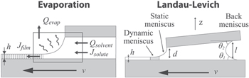
Fig. 6. Schematic illustration of the two deposition regimes in MGC methods. Reprinted with permission from Ref. 52 Copyright 2009 American Chemical Society.
Download figure:
Standard image High-resolution image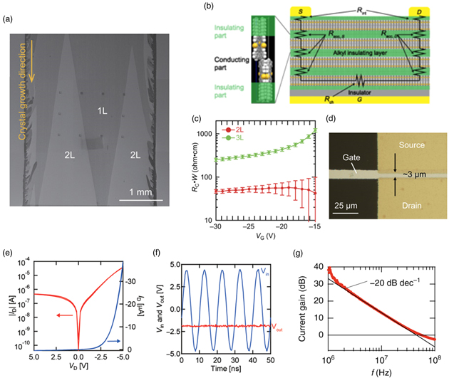
Fig. 7. (Color online) Demonstration of high-speed OTFTs based on printed 2L single crystals of Cn -DNBDT-NW (n = 8 or 9). (a) Combined scanning tunneling microscopy image of the 1L−2L mixed single-crystal thin film. Reprinted with permission from Ref. 50 Copyright 2018 American Association for the Advancement of Science. (b) Schematic model of contact resistance for single-crystal OTFTs composed of layered alkyl chains and π-conjugated cores. Reprinted with permission from Ref. 54 Copyright 2017 American Physics Society. (c) Contact resistance of 2L and 3L OTFTs and (d) an optical microscope image of the short-channel transistor with L = 3 μm. Reprinted with permission from Ref. 50 Copyright 2018 American Association for the Advancement of Science. (e) Current−voltage characteristics and (f) input and rectified output signals (100 MHz) of a diode-connected 2L OTFT with L = 1.5 μm. Reprinted with permission from Ref. 55 Copyright 2020 Wiley-VCH GmbH. (g) Estimation of fT of a 2L OTFT with L = 1.5 μm and LC = 1 μm (fT = 45 MHz) by an S-parameter analyzer. Reprinted with permission from Ref. 56 Copyright 2020 Springer Nature.
Download figure:
Standard image High-resolution imageThe blade width is a crucial factor to determine the coverage area and the overall uniformity of the single crystals and the integrated circuit design (Fig. 8). Starting research on CEC with a 20 mm wide homemade blade, 49) a 1 mm wide blade was designed to separately and alternately paint p-type and n-type organic semiconductor single crystals on the same substrate, 58) where the length of the single crystals can be larger than a few centimeters. This technique allowed printed single crystal-based complementary D flip-flop circuits and an RFID tag that can operate at 13.56 MHz. On the other hand, wider blades are indispensable for fabricating ultimately large-area single crystals. This principle was demonstrated by a 90 mm wide blade and the sophisticated organic semiconductor material C9-DNBDT-NW. 51) The printing principle is basically the same as the conventional CEC shown above [Figs. 9(a), 9(b)], whereas an increase in the size of the blade may need that of the whole setup by a customized instrument rather than a homemade one. With some appropriate conditions, a single crystal can be grown in the large area of 90 mm by 90 mm with the approximate thickness of 10 nm, corresponding to a few molecular layers. Noting more details, parameters described in Fig. 9(b) have been classified into two groups. Group 1 includes Tsol, Tsuppl and Tblade, which are temperatures of the bath for semiconductor solution, the solution supply line between the bath and a blade, and the blade, respectively. They do not appear in general MGC rather than CEC because those parameters are specifically used for keeping a large amount of organic semiconductor solution outside of the printing regime homogeneous and close to Tsub in temperature. In principle, the parameters in group 1 are crucial for a continuous supply of the semiconductor solution with a certain concentration and accept a variation of 10 °C as long as they are comparable to or moderately higher than Tsub. Group 2 includes COSC, Tsub, vsub and csuppl, where csuppl approximately corresponds to Qsolvent in Fig. 6. The parameters in group 2 control the thickness of single-crystal thin films according to the theory in the evaporation regime (Fig. 6); hence, they should be precisely optimized and controlled to uniform, large-area single-crystal thin films. Besides, COSC was as low as 0.02 wt% to reduce the frequency of undesired crystal nucleation, which would lead to polycrystals, whereas vsub was 15 μm s−1, and the maximum system temperature was 110 °C for Tsol. Finally, 3L crystals were printed on an insulating polymer-coated silicon wafer substrate with Tsuppl of 88 °C, Tblade of 84 °C, Tsub of 88 °C and csuppl of 0.51 μl s−1 [Fig. 9(c)]. Furthermore, a top-contact/bottom-gate OTFT array composed of 1600 elements was fabricated to validate the quality of the single-crystal thin film [Fig. 9(d)], where the top-contact Au pads were photolithographic patterned and each OTFT was isolated by laser ablation to avoid misestimation of the carrier mobilities due to fringe current effect. 59) The map of hole mobility is shown in Fig. 9(e), where the coordinates correspond to Fig. 9(c). As summarized in Figs. 9(f)–9(g), selected 864 OTFTs [highlighted by an orange square in Fig. 9(c)] exhibited the average mobility of 10.1 cm2 V−1 s−1 (standard deviation 0.73), demonstrating a scalable fabrication of reproducible, high-performance OTFTs promising for the high-end devices in the near future. On the other hand, Fig. 9(e) provides additional information: lower mobility values (white and bluish colors) were located at left-side, upside, and downside edges, i.e. outside of region including the 864 OTFTs. Because the left side corresponds to the initial part of printing, the lower mobility is attributed to a non-uniform film due to unsteady crystal growth conditions at the initial stage of printing. Besides, the other regions correspond to the side edges of the blade, where the evaporation of the solvent is not fixed to the printing direction. Thus, these undesired regions are not usually suitable for uniform single crystal growth. By contrast, in the region of the 864 OTFTs, namely the sweet spot, the meniscus and solvent evaporation are under an optimum set of processing parameters; hence, the crystal growth enters a steady state. If once the steady state is established, it can be realized to avoid new nucleation and make the crystal thicker by controlling the parameters in group 2. Figure 9(h) schematically illustrates the formation of the ideal single crystal by CEC based on the experimental observations. This is a critical finding for realizing industrial systems of large-area single-crystal electronics because the results indicate that the principle of CEC is able to make infinitely continuous single crystals along the direction of movement of the stage. Thus, although a flat stage with fixed dimensions is used at the present, the CEC may be combined with mass-producible systems such as roll-to-roll carrier instruments.
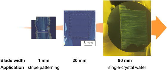
Fig. 8. (Color online) Scalability of the CEC method from 1 to 90 mm in width with more than a few centimeters in length. Photos are reprinted with permission from Ref. 58 (Copyright 2017 Wiley-VCH GmbH), Ref. 69 (Copyright 2020 Springer Nature) and Ref. 50 (Copyright 2018 American Association for the Advancement of Science).
Download figure:
Standard image High-resolution image
Fig. 9. (Color online) Scalable single-crystal wafer and reproducible OTFT array. [(a), (b)] Schematic illustrations of the CEC setup. (c) Confocal microscopy image of the as-printed 90 mm by 90 mm C9-DNBDT-NW crystal. (d) Photograph of the OTFT array (1600 transistors) with photolithographic patterned, top-contact Au electrodes. (e) Mobility map for all 1600 OTFTs. The coordinates correspond to (c). (f), (g) Transfer curves of the 864 OTFTs (surrounded by a yellow dotted line in (c)) measured in air. Reprinted with permission from Ref. 51 Copyright 2019 Springer Nature. (h) Schematic illustration of the large-area growth mechanism of organic semiconductor single crystals by CEC.
Download figure:
Standard image High-resolution image
In Ref. 51, CEC was also proposed to reduce manufacturing costs. In terms of a time-cost issue, if a required coverage area is defined by the product of substrate length (lsub) and width (wsub), the total deposition time by CEC is predominantly determined by lsub wsub/wblade vsub (wblade: the width of blade), which can be further approximated to lsub/vsub when wblade ≈ wsub. Based on the reported optimum condition of vsub = 15 μm s−1, a 2D crystal of C9-DNBDT-NW in dimensions of 10 cm by 10 cm can be produced in 111 min, which also implies a printed length of the 2D crystal could be expanded to 120 cm per day in the upper limit, whereas the areal coverage can be further increased by developing the printing instrument and wider blades. In contrast, other printing methods which require a wide area scan, such as inkjet printing, need the time dependent on lsub wsub/vscan, where vscan stands for scanning speed. Hence, if one tries to deposit organic semiconductors over a certain area of lsub wsub, CEC does not depend on wsub whereas inkjet printing does, indicating that CEC would get superior with increasing the area and the degree of integration. Note that the multi-head inkjet printing technique can overcome this issue. Yet, in principle, any inkjet printing techniques form a considerable amount of useless, low-quality regions due to the coffee ring effect. On the other hand, CEC could yield seamless semiconductor films over a wide area, which would be useful for integrated circuit applications in higher integration densities. Thus one can select the appropriate technique depending on the circuit design, semiconductor material, etc. Besides, the heating cost may be additionally necessary, while it has a trade-off relation with a time-saving benefit. As for a materials cost issue, some material should be wasted by an etching process to minimize OTFTs and to avoid crosstalk if large-area continuous films (single crystals) are utilized. However, the waste rate can be reduced if OTFTs are integrated with higher and higher densities, i.e. the total active area is much larger than the etching area. In addition, the thickness-controlled 2D single crystals are advantageous from the viewpoint of materials consumption as declared in the introduction. For instance, the areal coverage of 100 cm2 by a 3L single crystal of C9-DNBDT-NW is ideally satisfied by approximately only 100 μg of the material.
5. Summary and outlook
In this Review, we have shown the progress in the technology of printed organic semiconductors with a special focus on large-area 2D single crystals. OTFTs based on the printed 2D single crystals promise a variety of advantages compared to traditional OTFTs: from a physical viewpoint, the large single crystals can maximize the electrical performances of semiconductor materials, such as carrier mobility and reproducibility, whereas, from an engineering viewpoint, low cost and materials consumption could be achieved. Also, from a chemical point of view, the MGC methods including CEC are compatible with the deposition of crystalline films composed of two or more molecular components, such as organic semiconductor-molecular dopant mixtures, 60) charge-transfer complexes, 61) and small-molecule/insulating-polymer biphase systems. 44,62–64) Hence, it can be expected that the MGC methods meet more fascinating 2D materials. Moreover, the 2D single crystals can be used as large-area membranes attachable to various substrates and objects, being extensively applicable for film devices. 65) Besides, potential applications of 2D single crystals are not limited to TFTs but able to be extended to advanced devices, such as flexible strain sensor 66) and organic p–n heterojunction devices. 67) In the future, it is highly hoped that further developments and understandings of printed 2D organic semiconductor single crystals as well as their integration technology to high-end devices will lead to a bright future for the IoT society.
Acknowledgments
We would like to thank the editorial office of Applied Physics Express for giving us an opportunity to contribute to APEX Review.
Biographies

Shohei Kumag ai received his Ph.D. degree in science in 2016 from Tohoku University under the supervision of Professor Masahiro Yamashita. In 2016, he was appointed the Japan Society for the Promotion of Science (JSPS) fellowship at The University of Tokyo, where he was promoted to a project assistant professor in 2018. His research interests include solid-state chemistry and transistor application of organic and amorphous-oxide semiconductors.

Tatsuyuki Makita is working at Pi-Crystal Inc. He received his Ph.D. in science from the University of Tokyo in 2021 under the supervision of Professor Jun Takeya. His research interests include the fabrication and application of thin-film organic semiconductors for integrated circuits.

Shun Watanabe is an Associate Professor in the Department of Advanced Materials Science at the University of Tokyo. He received his Ph.D. in materials science from Nagoya University in 2011, then carried out postdoctoral research on charge and spin transport physics in organic semiconductors at the University of Cambridge. In 2016, he started his independent research career at the University of Tokyo as a principal investigator. His research focuses on materials science in solution-processable organic semiconductors and condensed matter physics, with the goal of potential applications in printable optoelectronic devices.

Jun Takeya is a Professor in the Department of Advanced Materials Science, Graduate School of Frontier Sciences, University of Tokyo from 2013 and is jointly appointed as an honored visiting researcher in National Institute for Material Science from 2017. He is also CTO of Pi-Crystal Inc. from 2013 and Organo-Circuit Inc. from 2016 which are start-ups founded on his scientific achievement in organic electronics. He received a B.S. degree in 1989, an M.S. degree in 1991, and a Ph.D. degree in 2001 from the University of Tokyo, Tokyo, Japan, all in physics. He was a research scientist at the Central Research Institute of Electric Power Industry, from 1991 to 2006, a visiting researcher in ETH, Zurich, Switzerland, from 2001 to 2002, a visiting researcher in RIKEN, Japan, from 2005 to 2006, a visiting associate professor in IMR, Tohoku University, Japan, from 2005 to 2006, and an associate professor in Graduate School of Science, Osaka University, Osaka, Japan, from 2006 to 2010. He was a professor at the Institute of Scientific and Industrial Research, Osaka University, Osaka, Japan, from 2010 to 2013.