
Abstract
A ScAlN thin film is one of the key materials of MEMS and high-frequency filters used in new-generation communication devices. Piezoelectricity can be improved by increasing Sc concentration. However, abnormal grains often appear at high Sc concentrations, degrading crystallinity and piezoelectricity. Herein, we demonstrated that underlayer roughness considerably affects the emergence of abnormal grains in a Sc0.4Al0.6N thin film formed via reactive DC sputtering. Dry etching with Ar plasma can effectively reduce the surface roughness of amorphous SiN and polycrystalline Si. Sc0.4Al0.6N thin films deposited on amorphous SiN and polycrystalline Si with sufficient flat surfaces exhibited a low density of abnormal grains, high crystallinity and piezoelectricity, and low loss tangent. Moreover, such high-quality thin films were obtained on a borophosphosilicate glass flattened using a reflow process without Ar etching. Therefore, underlayer roughness played an important role. The findings can help enable the large-scale production of highly doped ScAlN thin films.
Export citation and abstract BibTeX RIS

Content from this work may be used under the terms of the Creative Commons Attribution 4.0 license. Any further distribution of this work must maintain attribution to the author(s) and the title of the work, journal citation and DOI.
1. Introduction
Aluminum nitride (AlN) thin films have been used as piezoelectric transducer materials in various microsystems owing to their superior and unique characteristics. For example, its high sound velocity, low dielectric loss, and compatibility with standard CMOS processes have made this material a dominant player in bulk acoustic wave (BAW) devices for high-frequency filters. With the recent global spread of mobile communication, the market for AlN thin films has grown to be one of the largest in MEMS. 1)
Moreover, Akiyama et al. demonstrated that the piezoelectricity of AlN thin films can be significantly improved by partially replacing the Al sites of AlN with Sc. 2) Basically, the higher the concentration of Sc in all metal atoms, the higher the piezoelectricity of ScAlN. They successfully demonstrated that the piezoelectric coefficient d33 at a Sc concentration of 43% reaches approximately five times that of an intrinsic AlN thin film. Many subsequent studies have been conducted, including first-principles calculations, film characterization, and application to a variety of devices. 3–8) ScAlN thin films have already been put to commercial use in recent BAW devices because they can increase the bandwidth. 9–13)
However, the mass-production of ScAlN thin films with a Sc concentration of approximately 40% or higher is difficult in practice. One reason for this is that abnormal grains are easily generated when the Sc concentration is increased. 14–18) Piezoelectric materials with wurtzite structures, such as AlN and ZnO, show the highest piezoelectricity when oriented along the c-axis. However, the abnormal grains are not oriented along the c-axis, leading to a decrease in piezoelectricity. 14,17) Abnormal grain growth (AGG) has also been reported in AlN and ZnO, 19–21) and is more pronounced in ScAlN at high Sc concentrations. The AGG in ScAlN thin films is an obstacle to increasing the concentration.
To date, the mechanisms behind AGG have not been elucidated. However, many experimental facts and hypotheses have been reported, which may lead to the elucidation of this mechanism. For example, AGG is correlated with the internal stress of the film. 15,22) In addition, plasma etching of the underlayer before the deposition of an AlN-based thin film was reported to suppress it. 14,20) The report in Ref. 20 claims that the removal of surface contaminants contributes to suppression. However, AGG often occurs even with the continuous deposition of an underlayer and AlN-based thin film, where contamination is less likely to occur. Therefore, the claim is questionable.
On the other hand, there are several reports on the promotion effect of plasma pretreatment on the c-axis of an intrinsic AlN thin film. 23–26) That is potentially due to the induction of microdefects on the surface, 23,24) modifying the surface to be amorphous, 25) removing contaminants, 20) or decreasing the surface roughness. 26) However, these reports do not refer to AGG suppression. Plasma pretreatment promoted c-axis orientation; however, this could be unrelated to AGG.
We hypothesize that the AGG of ScAlN is strongly influenced by slight differences in the surface roughness of the underlayers. The arithmetic mean roughness (Ra) is on the order of subnanometers, which optically is sufficiently mirror-like. Plasma pretreatment probably reduces the surface roughness, resulting in the suppression of AGG.
In this study, we verified this hypothesis by depositing and characterizing ScAlN thin films on three different material layers: SiN, polycrystalline Si (poly-Si), and borophosphosilicate glass (BPSG). First, ScAlN was deposited on an amorphous SiN underlayer treated with Ar-plasma etching for an arbitrary time. The use of such an amorphous layer should eliminate the aforementioned causal hypothesis based on defect formation and amorphization induced by plasma pretreatment. Consequently, the increase in the plasma etching time flattened the SiN underlayer, resulting in an improvement in the crystallinity, piezoelectricity, and loss tangent of the ScAlN thin film. Next, such an improvement was demonstrated in the case of a poly Si underlayer. Furthermore, this was observed even when the BPSG underlayer was planarized by a reflow process rather than plasma treatment. Thus, we demonstrate that flattening the underlayer is effective in suppressing AGG for both crystalline and amorphous materials, and the flattening method does not require plasma treatment.
2. Experimental methods
2.1. Deposition of an amorphous SiN underlayer
First, a 25 nm thick Mo layer was deposited as the bottom electrode on a 6-inch Si substrate using a DC sputtering system. Subsequently, a 30 nm thick SiN layer was deposited using plasma-enhanced CVD (AMAT P5000). The deposition conditions were as follows: SiH4:36 sccm, NH3:26 sccm, and N2:2250 sccm were used as the introduced gas with a gas pressure of 688 Pa, substrate temperature of 333 °C, and RF power of 303 W.
Next, the SiN surface was etched using dry etching equipment (AMAT P5000). Ar:50 sccm was used as the introduced gas at a pressure of 2 Pa and an RF power of 50 W. The substrates were not heated. The film thicknesses before and after the Ar etching were measured using an ellipsometer, giving an etching rate of 0.17 nm s−1. The roughness before and after etching was evaluated using a scanning probe microscope (SPM; Shimadzu SPM-9700) and a cantilever (Olympus OMCL-AC200TS-C3) in dynamic mode. A 500 nm square area was scanned with a resolution of 256 × 256 points, and the arithmetic mean roughness (Ra) was determined from the two-dimensional topographic data.
2.2. Deposition of a poly-Si underlayer
A 60 nm thick poly-Si layer was formed on the Si substrate using thermal CVD. SiH4, PH3, and N2 gases were introduced, the temperature was set to 580 °C, and the gas pressure was set to 30 Pa. The poly-Si was doped with phosphorus to increase its conductivity, allowing it to function as a bottom electrode. The surface was treated with Ar etching in the same manner as the SiN underlayer.
2.3. Deposition of a BPSG underlayer
A 70 nm thick BPSG underlayer was deposited directly on the Si substrate using ozone-CVD equipment (AMAT P5000). Si(OC2H5)4, B(OC2H5)3, C6H15O4P, O3, and N2 were used as source gases. The pressure and the temperature of the substrate were set to be 2.7 × 10⁴ Pa and 480 °C, respectively. The BPSG surface was flattened by a reflow process without plasma treatment. This allowed us to determine whether the suppression of AGG was due to the surface roughness of the underlayer or the plasma treatment. The reflow process was performed in a quartz tube furnace at 900 °C for 20 min under a nitrogen atmosphere.
2.4. Deposition of a ScAlN layer
A ScAlN thin film was deposited on each underlayer using a parallel-plate reactive DC sputtering system (ULVAC SME-200E). The target was a 300 mm diameter Sc0.4Al0.6 alloy fabricated by sintering. The deposition conditions were as follows: the introduced gas was N2:26 sccm and Ar:19 sccm at a pressure of 0.3 Pa, a substrate temperature of 400 °C, DC power of 8 kW, and RF power applied to the substrate susceptor of 20 W. RF power was applied to improve the film crystallinity by increasing the energy of the ions incident on the film. The deposition thickness of the films was 500 nm. The composition ratio of Sc/(Sc+Al) in the ScAlN film was measured to be 40 ± 1% by Rutherford backscattering spectrometry (RBS).
2.5. Characterization methods for ScAlN thin films and underlayers
The crystallinity of the ScAlN thin films deposited on each underlayer was evaluated using an X-ray diffractometer (Philips X'Pert MRD). The surface morphology was observed using scanning electron microscopy (SEM; JEOL JSM-IT510LV) to evaluate the density of abnormal grains.
To evaluate the electrical and piezoelectric properties, a 300 nm thick Al pattern with a diameter of 3 mm was fabricated on the ScAlN thin film as the topside electrode. A 20 nm thick Ti adhesion layer was utilized at the interface between the ScAlN thin film and the Al layer. In addition, Al/Ti layers with thicknesses of 700/20 nm were deposited on the back and sides of the chip to serve as terminals for the bottom electrode. The piezoelectric coefficient d33, loss tangent, and leakage current versus voltage were measured using a d33 meter (Piezotest PM2000), an impedance analyzer (Agilent 4195 A), and a semiconductor parameter analyzer (HP 4156 B), respectively.
To estimate the defects in the ScAlN thin films, cathodoluminescence (CL) measurements were performed at room temperature using a SEM (JEOL JSM-7800F) equipped with CL apparatus (HORIBA MP-32S). The acceleration voltage and probe current were set as 10 kV and 11 nA, respectively.
3. Results and discussion
3.1. Deposition of a ScAlN thin film on an amorphous SiN layer
3.1.1. Effect of Ar etching on the SiN layer and analysis of the crystalline quality, orientation, and morphology of the ScAlN thin film
Figure 1 shows topographic images of the SiN surface before and after Ar-plasma etching. The as-deposited SiN surface exhibited a mound aggregation morphology with individual mounds—10–20 nm in diameter, as shown in Fig. 1(a). SiN deposited by the CVD process is reported to have such a morphology. 27) As shown in Figs. 1(b)–1(d), the contours of the individual mounds became unclear as the etching time increased. The Ra values in this area also decreased, as shown in Fig. 2. The SiN surface was planarized via Ar etching. In general, such planarization is attributed to the dependence of sputtering yield on the angle of ion incidence. This results in faster etching of the inclined planes on an uneven surface, with the convex areas becoming sharper and the concave areas flattened. In other words, the surface may be planarized by the lateral movement of the sloped surface region. 27,28)
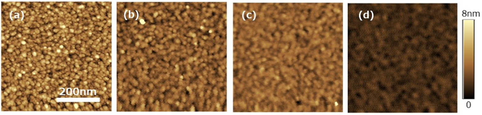
Fig. 1. Scanning probe microscopy images of the SiN surface after Ar etching, with etching times of (a) 0 s, (b) 15 s, (c) 30 s, and (d) 90 s. The scanning area size and roughness scale are consistent across all images.
Download figure:
Standard image High-resolution image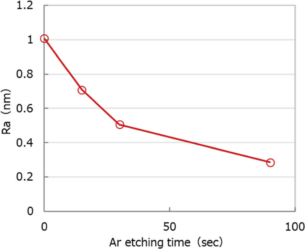
Fig. 2. The arithmetic mean roughness (Ra) of the SiN surface over Ar etching time.
Download figure:
Standard image High-resolution imageFigure 3 shows X-ray diffraction (XRD) results for ScAlN thin films on SiN layers treated with different Ar etching times. The crystallinity of the ScAlN thin film improved with increasing etching time. In the 2θ-ω scan of Fig. 3(a), the peaks around 36.5°, which correspond to the ScAlN (0002) diffraction, were observed in the specimens treated with Ar etching. Thus, the treated films exhibit a preferential c-axis orientation. The peak positions shifted slightly to lower angles as the etching time increased. This shift might indicate that the film stress shifted toward the compressive side. As shown in Fig. 3(b), the peak intensity increased, and the FWHM of the rocking curve of the (0002) diffraction decreased with increasing etching time. However, the fluctuations became saturated at 90 s. The FWHM reached 1.7° after saturation. Therefore, ScAlN thin films with higher crystallinity and c-axis orientation tend to grow on SiN surfaces planarized by Ar plasma etching.
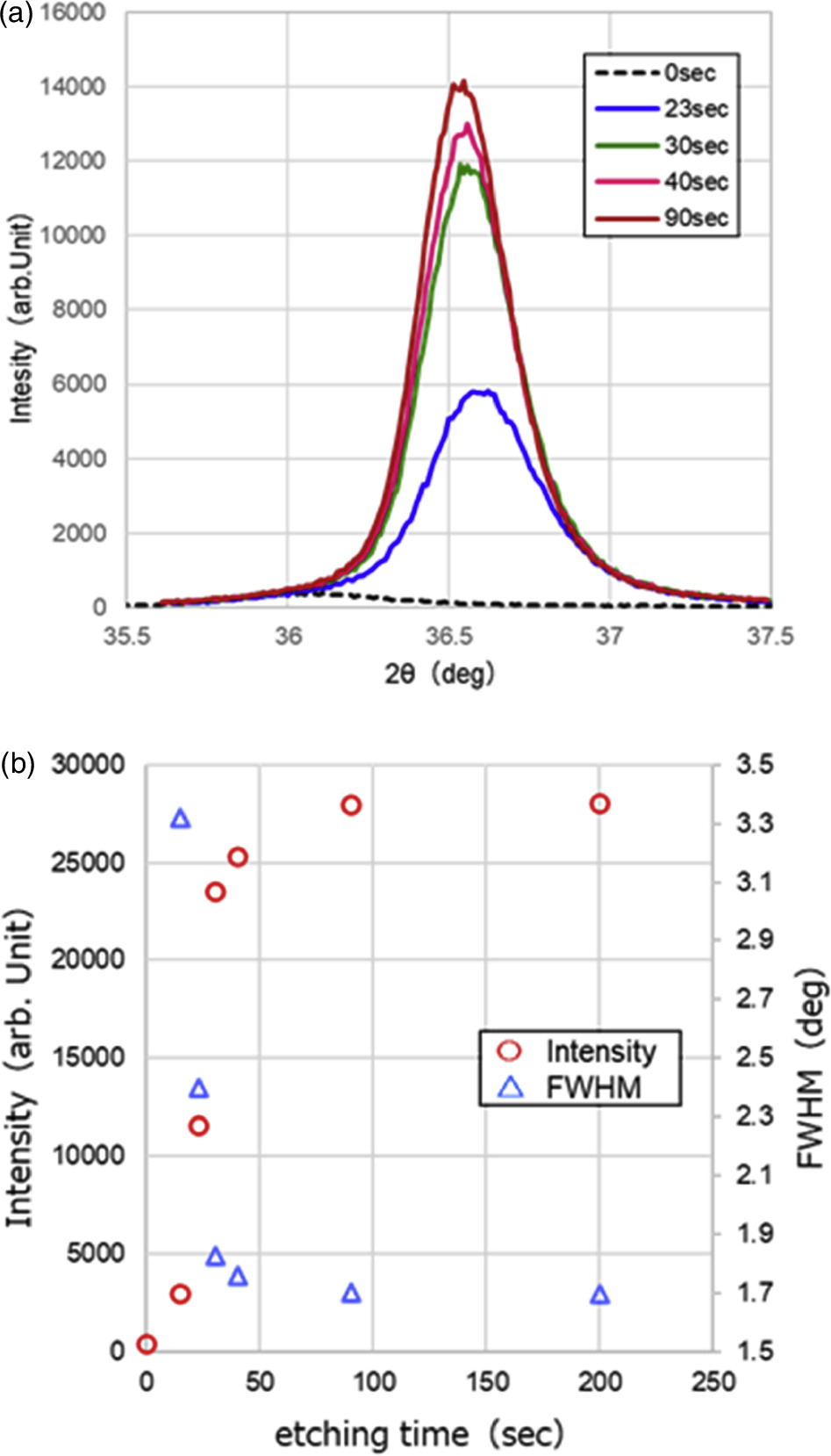
Fig. 3. X-ray diffraction analysis of Sc0.4Al0.6N film on SiN with different Ar etching times. (a) 2θ-ω scan patterns. (b) Intensity and FWHM of rocking curve versus etching time.
Download figure:
Standard image High-resolution imageBecause the (0002) plane in the wurtzite-type structures of AlN and ScAlN is the most stable, the growth of a c-axis oriented thin film on the surface of such an amorphous material is reasonable. Interestingly, slight differences in the surface roughness significantly changed the crystallinity and orientation. The Ra values of the SiN surfaces were 1 nm and 0.3 nm before and after the 90-s etching, respectively. The former already had a mirror-like surface; however, even slight roughness inhibited the crystallization of ScAlN.
As shown in Fig. 4(a), abnormal grains were observed in the entire surface of the ScAlN thin film on the SiN layer before etching. However, the grain density decreased with increasing etching time [Figs. 4(b) and 4(c)]. This result is consistent with the XRD results.

Fig. 4. Surface scanning electron microscopy images of Sc0.4Al0.6N films on SiN with different Ar etching times of (a) 0 s, (b) 30 s, and (c) 90 s.
Download figure:
Standard image High-resolution image3.1.2. Measurement of the piezoelectricity, loss tangent and leakage current
Like the crystalline quality, the piezoelectric coefficient d33 increased with increasing etching time. As shown in Fig. 5(a), d33 reached approximately 22 pC N−1 for Ar etching times of 40 s or longer. This value is comparable to that reported in Ref. 2. Comparing Figs. 3 and 5(a) shows that the etching time was shorter than the time at which the crystallinity was saturated. This indicates that piezoelectricity does not necessarily require extremely high crystallinity. In addition, the presence of a small number of abnormal grains, as shown in Fig. 4(c), did not significantly degrade the piezoelectricity. The abnormal grain densities estimated from the SEM images were 16 and 9 μm−2 for etching times of 30 and 90 s, respectively. Therefore, abnormal grain densities of approximately 10 μm−2 is considered to be a guideline for sufficient piezoelectricity.
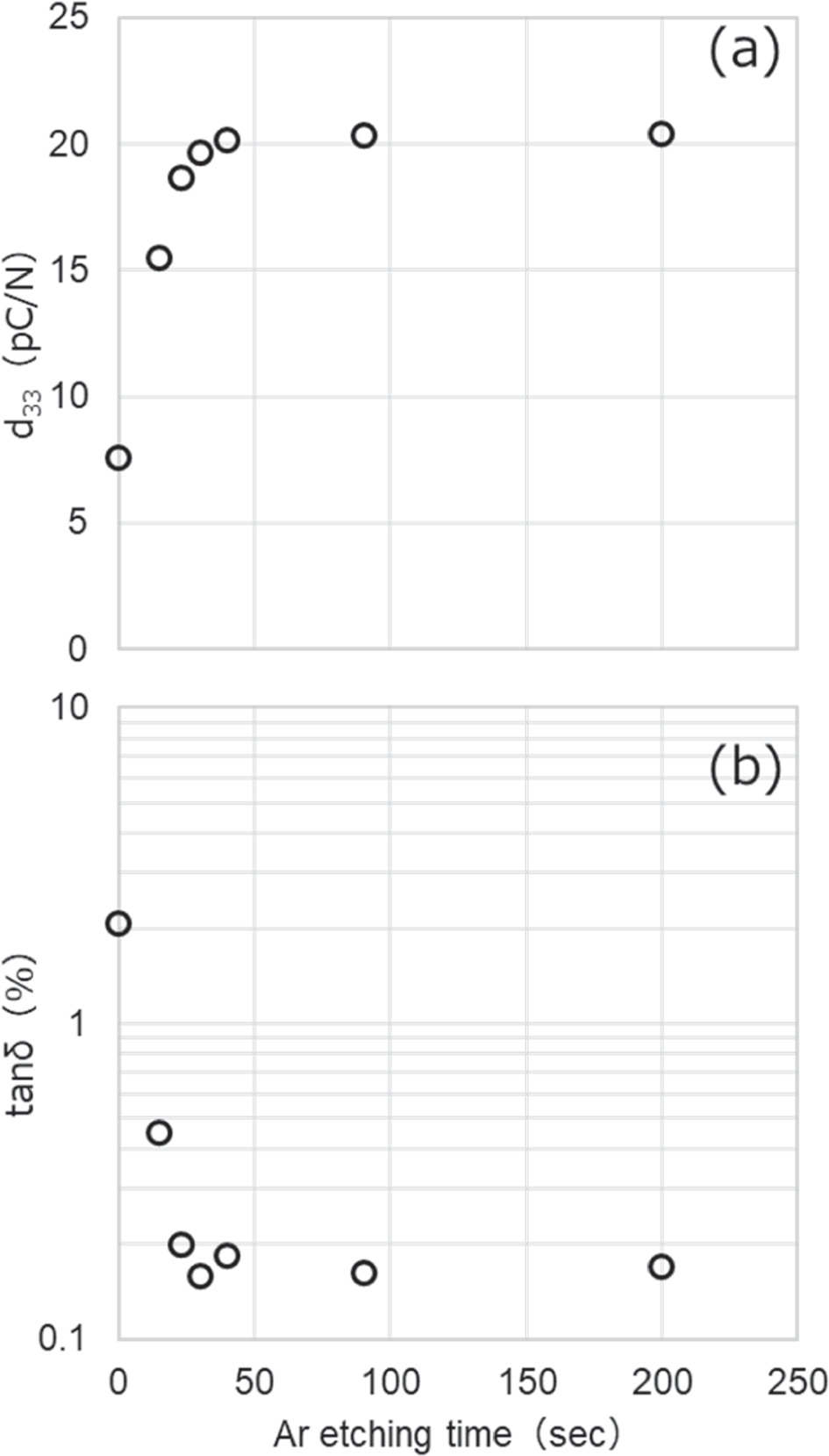
Fig. 5. (a) Piezoelectric coefficient d33 and (b) loss tangent at 1 kHz of Sc0.4Al0.6N over Ar etching time for SiN.
Download figure:
Standard image High-resolution imageFurther, the loss tangent also improved, i.e. lowered to approximately 0.2% after 30 s [Fig. 5(b)]. This value is smaller than that reported in a previous study at the same Sc concentration. 14) The causal factors increasing the loss tangent are probably within or at the grain boundaries of the abnormal grains, considering that Ar etching is accompanied by a decrease in the density of abnormal grains.
Figure 6 plots the current–voltage curves of the ScAlN thin films with and without Ar etching. The leakage current was significantly reduced by Ar etching but those after 23 s and 90 s long etchings were almost equivalent. This result is consistent with the fact that the piezoelectric constant and loss tangent become nearly constant when the Ar etching time exceeds 23 s, as shown in Fig. 5.

Fig. 6. Current–voltage characteristics of Sc0.4Al0.6N under different Ar etching times.
Download figure:
Standard image High-resolution imageTherefore, the Ar etching of the SiN underlayer demonstrably improved the crystallinity, piezoelectricity, loss tangent, and leakage current of ScAlN thin films. These important properties influence the performance of specific piezoelectric MEMS devices.
Inserting a non-piezoelectric SiN layer between the ScAlN thin film and Mo bottom electrode could reduce the effective piezoelectricity of the ScAlN film. However, this should not be a problem in practice for the following reasons: The drive voltage applied between the top and bottom electrodes is distributed between the ScAlN thin film and SiN layer. Consequently, the effective d33 value is smaller than the intrinsic d33 value of the ScAlN thin film. In this case, each distributed voltage is determined from the ratio of the capacitances of the two layers. Accordingly, a smaller thickness and higher dielectric constant of the nonpiezoelectric underlayer are preferable for applying a large drive voltage to ScAlN thin films. As shown in this study, a SiN layer that is much thinner than the ScAlN thin film can be deposited on metal electrodes owing to the low-temperature process of plasma-enhanced CVD. In addition, SiN has relatively high permittivity. Therefore, the decrease in d33 is not significant. SiO may also be another candidate for the underlayers.
3.1.3. Analysis by cathode luminescence (CL)
Figure 7 shows the emission spectrum of the CL used to estimate the defects in the ScAlN thin film. First, the band-edge emission peak derived from ScAlN was not observed at 270 nm. Note that this wavelength corresponds to approximately 4.5 eV as the band gap. 29) That may be due to the low crystallinity of the ScAlN thin film. In contrast, a broad peak consisting of four to five narrow peaks appears at wavelengths ranging from 200 to 800 nm. A similar broad peak is observed in other materials such as gallium nitride (GaN) crystals or thin films. In the case of GaN, such a broad peak is reported to be caused by defects in the material. 30,31) GaN is a III–V compound semiconductor material with a wurtzite structure similar to that of ScAlN. Thus, the broad peak in the spectrum of ScAlN is also attributed to defects. Multiple thin peaks appeared owing to multiple reflection interferences at the top and bottom surfaces of the ScAlN thin film. 30)
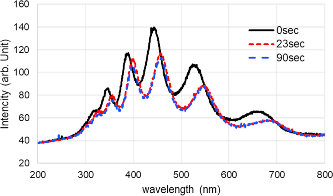
Fig. 7. Cathode luminescence spectra of Sc0.4Al0.6N under different Ar etching times on the underlayers.
Download figure:
Standard image High-resolution imageThe most important aspect of the spectra was the decrease in the intensity of the broad peak after Ar etching. This indicates that the number of defects in the film decreased. It is likely that defect reduction led to a reduction in the leakage current. In addition, increasing the Ar-etching time to 90 s did not lead to a further decrease in the intensity. Saturation behavior of the etching effect was observed, as was the case for the leakage current. Thus, the Ar-etched SiN underlayer contributes to the deposition of ScAlN with fewer defects.
3.2. Deposition of a ScAlN thin film on a poly-Si layer
Next, we investigated whether the above planarization effect occurs not only in SiN, but also in other underlying materials. The poly-Si surface was planarized by Ar etching in the same manner as the SiN described above. As shown in Fig. 8(a), the poly-Si layer had rounded grains of approximately 20 nm in diameter before Ar etching. After etching of 30 s, the contours of these grains disappear, leaving an uneven pattern with a smaller spatial frequency [Fig. 8(b)]. The Ra value decreased significantly from 1.14 to 0.37 nm as shown in Fig. 2.
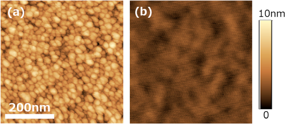
Fig. 8. Scanning probe microscopy images of the polycrystalline Si surface (a) before and (b) after Ar etching of 30 s. Scanning area size and roughness scale are unified.
Download figure:
Standard image High-resolution imageFigure 9 shows the XRD patterns of the ScAlN thin films deposited on poly-Si underlayers with and without Ar etching. The peak intensity of the (0002) plane in the ScAlN thin film deposited on the Ar-etched underlayer was approximately 60 times higher than that of the film deposited on the non-etched underlayer. The FWHM of the rocking curve of the (0002) plane also improved significantly from 5.5° to 1.7° after Ar etching. The former sample had many abnormal grains [Fig. 10(a)], whereas the latter had a smaller number of grains [Fig. 10(b)], as in the case of the SiN underlayer. The piezoelectric coefficient d33 also improved from 16 to 25 pC N−1 after Ar etching. The value of 25 pC N−1 is higher than that for the SiN underlayer. This is perhaps due to the direct contact between the ScAlN thin film and the poly-Si bottom electrode layer without an insulation layer, unlike in the case of the SiN/Mo bottom electrode.

Fig. 9. 2θ-ω scan pattern of Sc0.4Al0.6N on poly- Si.
Download figure:
Standard image High-resolution image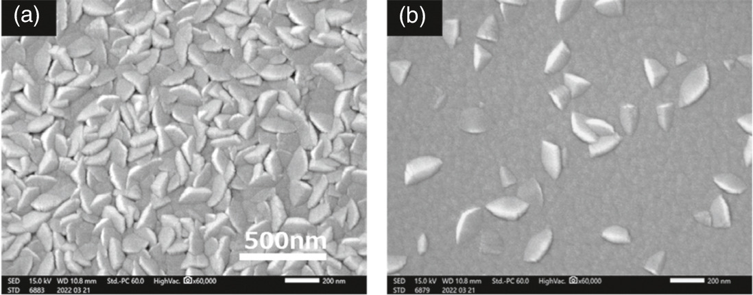
Fig. 10. Surface scanning electron microscopy images of Sc0.4Al0.6N on polycrystalline Si. (a) Without Ar etching and (b) with Ar etching.
Download figure:
Standard image High-resolution image3.3. Deposition of a ScAlN thin film on a BPSG
The abovementioned results demonstrate that the quality of ScAlN thin films is improved by Ar etching of both the SiN amorphous layer and poly-Si layer. In addition, to distinguish whether the improvement was due to surface roughness or another factor, a ScAlN thin film was deposited on a BPSG film with and without planarization by a reflow process based on thermal treatment.
Figure 11 shows topographic images of the surfaces of the BPSG thin films with and without the reflow processes. The surface of the as-prepared BPSG layer had a granular pattern with a diameter of less than several 10 nm. The Ra value was 0.42 nm and the surface was already mirror-like. After the reflow process, the granular pattern almost disappeared, and Ra decreased to 0.20 nm.
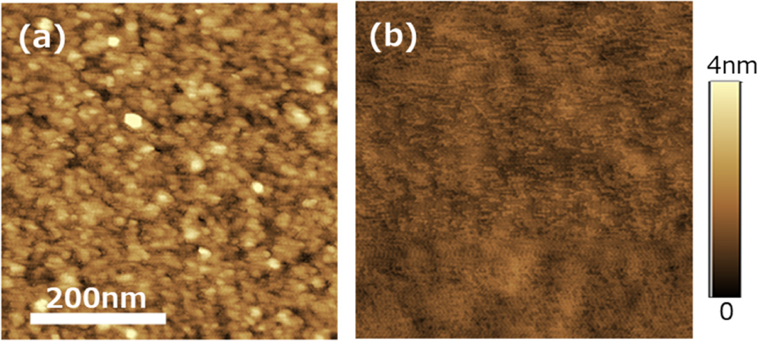
Fig. 11. SPM images of BPSG surfaces (a) without and (b) with reflow. The scanning area size and roughness scale are unified.
Download figure:
Standard image High-resolution imageScAlN films were then deposited on the BPSG layers with and without the reflow process. As shown in Fig. 12, the flatter BPSG layer provided a much higher crystallinity to the deposited ScAlN thin film. The FWHM of the rocking curve of the (0002) plane also improved from 3.8° to 1.9° owing to the reflow. The number of abnormal grains was also significantly reduced, as shown in Fig. 13.
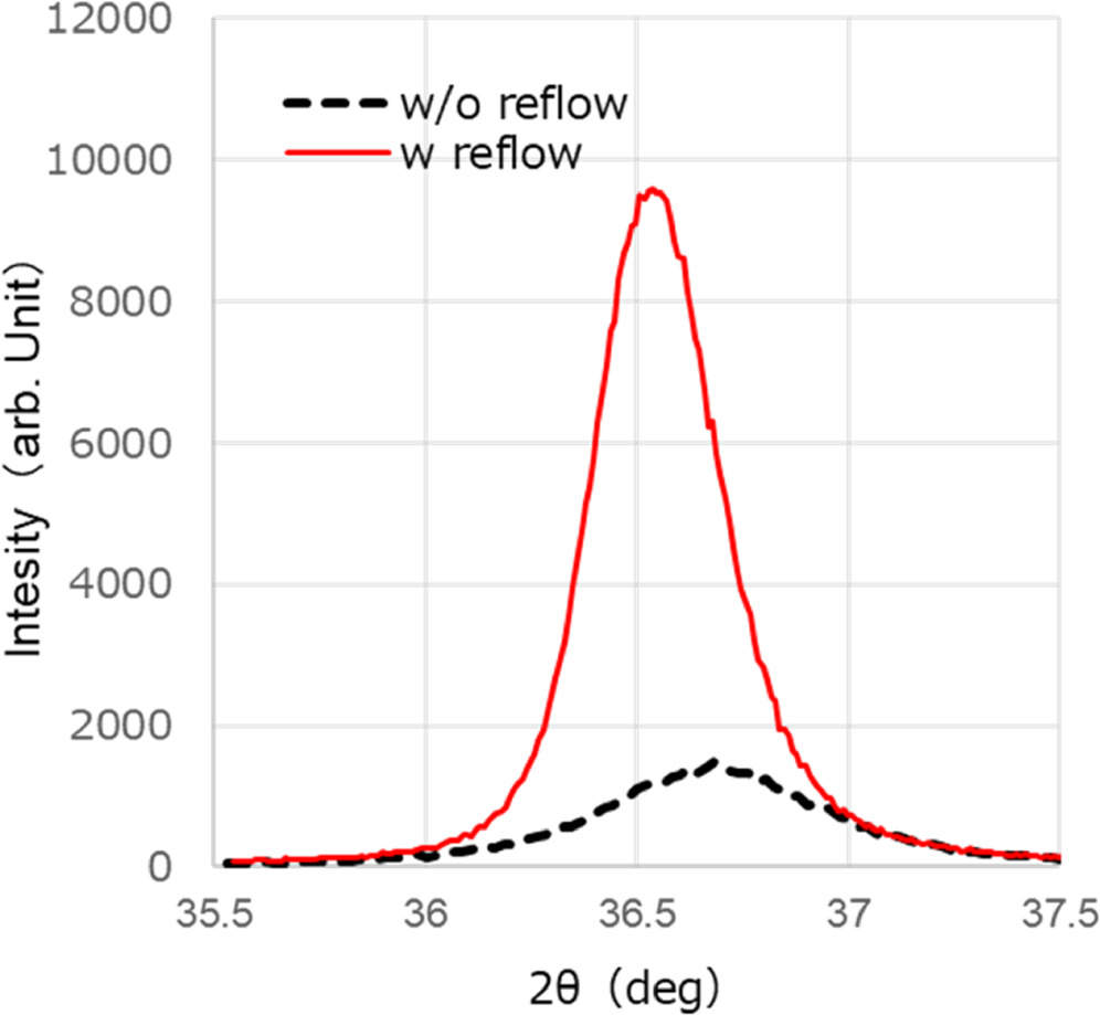
Fig. 12. 2θ-ω scan pattern of Sc0.4Al0.6N on BPSG.
Download figure:
Standard image High-resolution image
Fig. 13. Surface SEM images of Sc0.4Al0.6N on BPSG. (a) Without reflow (b) with reflow.
Download figure:
Standard image High-resolution image
The Ra value of 0.42 nm without reflow corresponded to that of the SiN surface after Ar etching for more than 30 s (Fig. 2). Thus, if only a small Ra value contributes to the enhancement of the crystallinity of the deposited ScAlN thin film, even the non-reflowed BPSG layer should provide much higher crystallinity for ScAlN. However, this was not the case. Thus, not only Ra, but also other factors may contribute to the improvement in crystallinity.
The SPM images of the BPSG without reflow [Fig. 10(a)] and SiN with an etching time of 30 s [Fig. 1(c)] have similar Ra values. However, the former exhibits a smaller grain size and a clearer grain outline. This indicates that each microscopic protrusion on the surface has a steeper slope. The steepness of the slope was not reflected in the Ra value. Such steep slopes are likely the starting points for abnormal grains. Therefore, an improvement in the crystalline quality of the ScAlN thin film was confirmed in the case of the reflowed-BPSG-underlayer with a smooth surface.
In summary, the abovementioned results clearly indicate that the roughness of the underlayer is a critical factor in determining the abnormal grain density and performance of the ScAlN thin film. Excellent flatness with a sub-nanometer-level Ra is required to achieve sufficiently high crystallinity and performance. The planarization method does not need to be Ar etching. In addition, it is unlikely that the reflow process created defects on the BPSG surface or removed surface contamination. This also supports the idea that the primary effect of Ar etching the underlayer is planarization of the surface.
4. Conclusions
We investigated why Ar etching of the underlayer is effective in depositing high-quality ScAlN thin films with 40% Sc concentrations. First, an amorphous SiN layer was used as a test specimen. We confirmed that Ar etching reduced the roughness of the layer and that the Ra value gradually saturated with increasing etching time. The ScAlN thin film deposited on the Ar-etched underlayer exhibited excellent crystallinity, high piezoelectricity, low loss tangent, small leakage current, and low density of abnormal grains. A CL analysis showed that the number of defects in the ScAlN thin film deposited on the Ar-etched underlayer was smaller than that on the non-etched underlayer. This phenomenon has also been observed in the case of poly-Si underlayers used as crystalline materials. Furthermore, a high-quality ScAlN thin film was successfully deposited on a reflowed-BPSG underlayer without Ar etching. This result supports the idea that the surface roughness is a significant factor in suppressing AGG and obtaining a ScAlN thin film with a high Sc concentration. In the experiments, when Ra decreased to approximately 0.5 nm, the abnormal grains were significantly reduced, the FWHM was as small as approximately 1.7°, the piezoelectric coefficient d33 was greater than 20 pC N−1, and the loss tangent was approximately 0.2%. These values are equivalent to or superior to those of previously reported Sc0.4Al0.6N thin films. The discovery and achievement of this study is a great step toward reproducibly creating a highly Sc-doped AlN thin film with excellent crystallinity and piezoelectric performance.
Acknowledgments
Part of this work was supported by the "Advanced Research Infrastructure for Materials and Nanotechnology in Japan (ARIM)" of the Ministry of Education, Culture, Sports, Science, and Technology (MEXT). Proposal Number: UT-0049. This work was also supported in part by JSPSKAKENHI Grant No. 22H01925.
We would like to thank Editage (www.editage.jp) for English language editing.