
Abstract
Ge-on-Insulator (GOI) is considered to be a necessary structure for novel Ge-based devices. This paper proposes an alternative approach for fabricating GOI based on the Ge-on-Nothing (GeON) template. In this approach, a regular macropore array is formed by lithography and dry etching. These pores close and merge upon annealing, forming a suspended monocrystalline Ge membrane on one buried void. GOI is fabricated by direct bonding of GeON on Si carrier substrates, using an oxide bonding interface, and subsequent detachment. The fabricated GOI shows uniform physical properties as demonstrated using micro-photoluminescence measurements. Its electrical characteristics and cross-sectional structure are superior to those of Smart-CutTM GOI. To demonstrate its application potential, back-gate GOI capacitors and MOSFETs are fabricated. Their characteristics nicely agree with the theoretically calculated one and show typical MOSFET operations, respectively, which indicates promising Ge crystallinity. This method, therefore, shows the potential to provide high-quality GOI for advanced Ge application devices.
Export citation and abstract BibTeX RIS
1. Introduction
Germanium (Ge) has attracted significant attention as a promising semiconductor material for the next generation of semiconductor devices due to its appealing characteristics, including high carrier mobility and a narrow bandgap corresponding to near-infrared wavelengths. 1,2) Thanks to substantial research efforts, fundamental processes like PN junctions, 3–5) gate stacks, 6–8) and metal contacts on Ge, 9–12) have been established for creating high-performance Ge-based MOSFETs, and NIR optical devices. 7,8,13–18) These foundational processing techniques have also been applied to innovative spintronic and quantum devices. 19,20)
Nonetheless, Ge devices face various challenges, such as substantial leakage currents due to the narrow bandgap, elevated material costs, and limited availability of raw materials. 21,22) To harness Ge's attributes in the benefit of the above-mentioned applications, Ge-on-Insulator (GOI) structures are necessary. Such a structure consists of a thin monocrystalline Ge layer, with a thickness ranging from several nanometers to several hundred nanometers, constructed on a support substrate with an intermediate insulator, commonly called buried oxide (BOX). Typical support substrates and BOX layers are silicon (Si) and silicon dioxide (SiO2), respectively. Several methods for producing GOI have been proposed, e.g. solid phase crystallization (SPC), 23,24) SiGe condensation, 25,26) wafer bonding with subsequent mechanical thinning, 27,28) and layer splitting at an ion-implanted depth, known as Smart-CutTM. 29–33) Each of the fabrication methods has advantages and disadvantages.
While the SPC method enables a straightforward production of Ge crystals, resulting materials are inherently polycrystalline, whose characteristics degrade due to the grain boundary. The SiGe condensation approach has the advantage of using a Si-on-Insulator (SOI) substrate, which is widely utilized in industry, as the starting material. However, the structures formed in this way often contain numerous residual defects originating from point defects or stacking faults. 34,35) In contrast, the wafer bonding method utilizes single-crystal bulk Si and Ge substrates as starting materials. After bonding both substrates using the BOX layer, a GOI can be achieved by thinning the bulk Ge. To maintain the original quality of the bulk Ge crystal, the thinning process must be performed without causing any damage. Additionally, the thinned Ge layer must possess adequate flatness for device fabrication. Mechanical polishing is a crucial technique for reducing the Ge thickness. The operation is carried out until the Ge thickness is reduced to several micrometers, followed by chemical mechanical polishing (CMP) for the final thinning and surface planarization. This method can yield GOI with low defect densities. However, ensuring thickness uniformity across a wafer scale represents a significant challenge. Another concern is the important Ge material loss during the thinning step. The Smart-CutTM method can more easily achieve wafer-scale uniformity thanks to an accurate control of the ion implantation depth. The bonded semiconductor substrate, post-hydrogen ion implantation, can be cleaved at the implanted depth through annealing or other external forces. 36) This method is widely employed for commercial SOI fabrication. Nevertheless, Ge is particularly sensitive to damages caused by ion implantation, and a complete repair of such damages remains a formidable task. 30,32,33,37,38) Therefore, an optimal approach for GOI fabrication is yet to be developed.
Recently, two labs have reported the successful fabrication of a Ge-on-Nothing (GeON) structure based on the reorganization of macro-porous Ge at high temperatures. 39,40) This method is based on the Si-on-Nothing fabrication suggested by Mizushima et al. 41) The GeON fundamental fabrication procedure is shown in Fig. 1. During high-temperature annealing following the formation of deep trenches by Ge dry etching, the top part of the macro-porous Ge reflows. Combining suitable deep trench dimensions (depth and density) and annealing conditions allows us to form a suspended monocrystalline Ge membrane still connected to the underlying layer by anchoring pillars present in a controlled and moderate density. The suspended Ge layer can then be transferred to another substrate, and the parent substrate can be reused multiple times. Using this GeON template, Depauw et al. practically demonstrated adhesive bonding and detachment of GeON to a glass substrate or soft material at the wafer scale. 21) Based on these former studies, an alternative method for fabricating high-quality GOI is being considered in this work. A Si substrate is used as a support substrate similar to SOI, and direct wafer bonding is used, instead of adhesive bonding. The obtained GOI films show better optical and electrical properties than those prepared by the usual Smart-CutTM approach. We presented that study at the 2023 International Workshop on Dielectric Thin Films for Future Electron Devices (IWDTF2023). 42) Compared to the previous report, more detailed results are presented in this article. First, the characterization of surface morphology using atomic force microscopy (AFM) is reported. Second, photoluminescence (PL) measurement results is discussed to evaluate the crystallinity of GOI. Third, the GeON-based GOI characteristics are compared with those of Smart-CutTM GOI. The obtained superior characteristics of GeON-based GOI in comparison to Smart-CutTM GOI suggest that this method can be a promising candidate for the fabrication of high-quality GOI for future Ge-based applications in many fields.
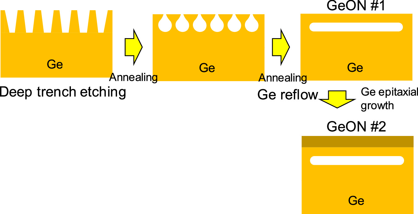
Fig. 1. Fabrication scheme for GeON on a bulk Ge substrate.
Download figure:
Standard image High-resolution image2. Experimental methods
Two types of GeON are fabricated from p-type (100) oriented, 6-degree offcut, 200 mm-Ge wafers, as listed in Table I and as described in Ref. 21. Sample #1 has a GeON thickness limited to ∼1 μm and a smooth surface. Sample #2 has a thicker GeON that was thickened by epitaxy, and a wavier surface. The GeON fabrication conditions lead to differences in resulting surface morphology. 43) Therefore, CMP is performed on #2 before bonding to smoothen its surface. Figure 2 summarizes the GOI fabrication procedure developed in this study. (100) oriented heavily doped p-type Si wafers are used as bonding Si substrates. The acceptor (active boron) concentration exceeds 1018 cm–3 and the bulk resistivity is ∼0.015 Ω·cm. After GeON surface cleaning in a diluted HF solution, a 3 nm thick Al2O3 layer is formed using atomic layer deposition. In parallel, an approximately 50 nm thick SiO2 film is thermally grown on the bonding Si substrate by dry O2 oxidation at 1000 °C, followed by N2 annealing at the same temperature to reduce the fixed oxide charge near the SiO2/Si interface. 44) After wet surface treatment, the GeON and Si are bonded manually in a class 1,000 cleanroom environment. To enhance the bonding strength, 0.3 MPa pressure is applied to the sample in a bonding vacuum chamber, followed by an anneal at 300 °C for 1 h. After these steps, the bonded GeON layer is detached by manually pulling the Ge substrate. The GOI layer is then thinned down and planarized by reactive ion etching and CMP. The thickness is measured by AFM and/or spectral reflectance thickness analyzer. The resulting GOI is characterized using micro-PL (μ-PL) and Hall effect measurements. For μ-PL, the excitation laser has a wavelength of 532 nm, a power of 20 mW, and a diameter of 2 μm. The structures were characterized using cross-sectional transmission electron microscopy (TEM). Thin foil samples were prepared for the TEM observations with a focused-ion beam sampling. The TEM observations were performed using a HD-2700 (Hitach High-Tech.) system.
Table I. Specifications of GeON for GOI fabrication in this study.
| GeON, GOI label | Conduction type of the starting Ge | GeON thickness | GeON surface | GOI evaluation methods |
|---|---|---|---|---|
| #1 | p | 1 μm | smooth | μ-PL |
| Hall effect | ||||
| Back-gate MOSFET | ||||
| #2 | p | 7 μm | wavy | Hall effect |
| Back-gate GOI capacitor |
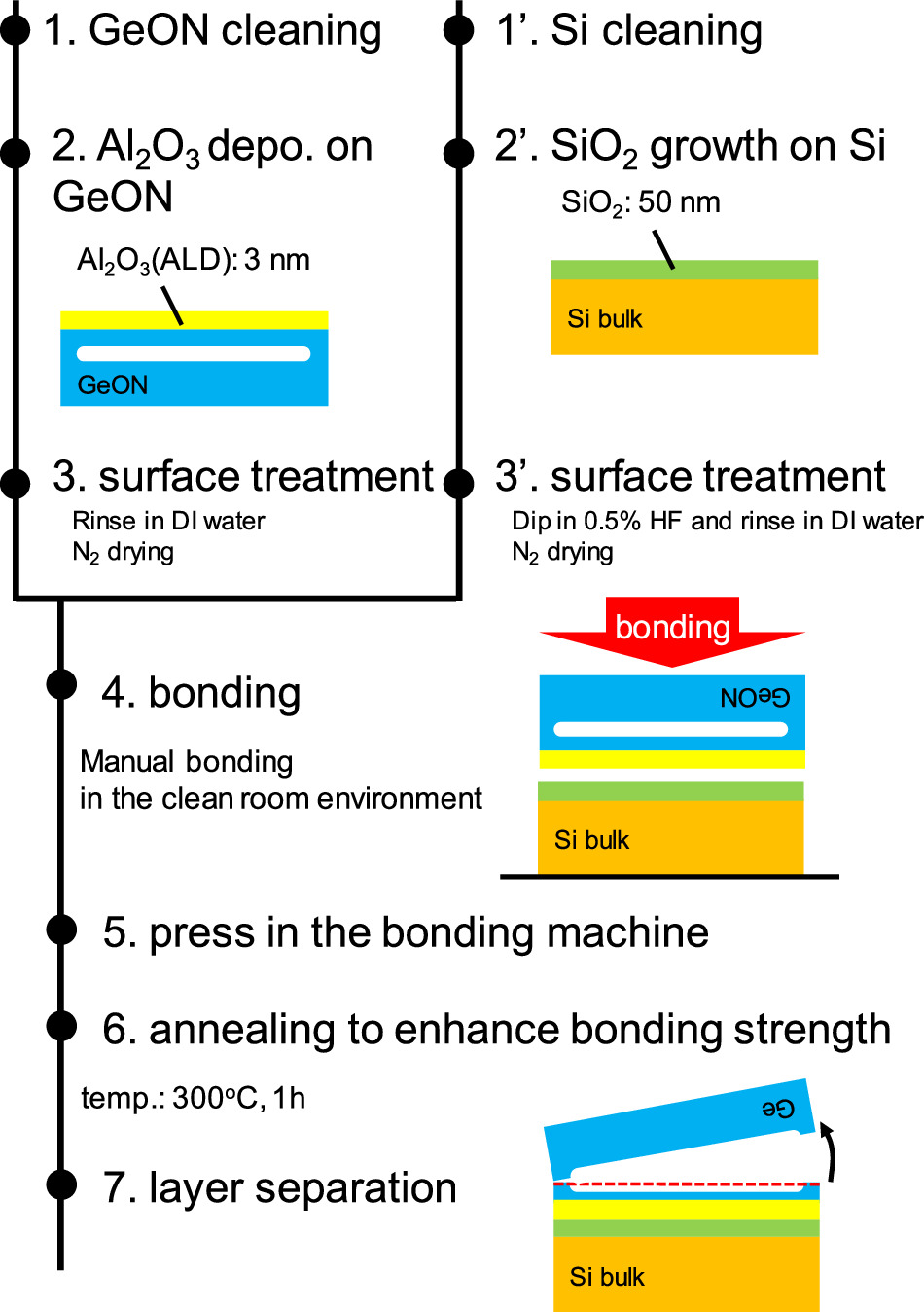
Fig. 2. Fabrication scheme for GOI based on GeON.
Download figure:
Standard image High-resolution imageTo enable a more detailed electrical characterization, back-gated GOI capacitors and MOSFETs are prepared. 45) Figure 3(a) shows the fabrication procedure of the back-gate GOI capacitor. After the GOI fabrication described above, a circular Pt electrode with a 50–240 μm diameter is formed by sputtering and lift-off techniques. An extra GOI layer around the Pt electrode is removed by wet etching using an H2O2-based solution. The backside (Si) ohmic contact is formed by In-Ga alloy rubbing. The fabrication scheme for the back-gate MOSFETs is shown in Fig. 3(b). First, the fabricated GOI is thinned by reactive ion etching. The active region is defined by wet etching creating a rectangular (156 μm × 55 μm) island shape isolation. Next, a metal S/D electrode is formed using sputtering and lift-off techniques. Pt is used as a hole injection electrode for accumulation mode p-MOSFET and TiN as an electron injection electrode for inversion mode n-MOSFET, respectively. 9,46) An Al layer is also deposited on Pt and TiN as contact pads. The resulting MOSFETs' channel length (L) and width (W) are 5–15 μm and 55 μm, respectively.

Fig. 3. Fabrication scheme for (a) back-gate GOI capacitor and (b) MOSFETs on GOI.
Download figure:
Standard image High-resolution image3. Results and discussion
3.1. Layer transfer and detachment
In this study, bonding experiments are carried out using several cm-square-large dies. Figure 4(a) shows the GeON and GOI labeled #1 after layer transfer and detachment. Although the whole area could not be transferred, we succeeded in transferring most of the area. There are two possible reasons. The first one is unexpected particle insertion during the bonding. It can be avoided using cleaner bonding equipment, such as a vacuum bonding machine used in commercial SOI production. The second one is the imperfect flatness of the GeON before bonding. 21) The surface roughness of the GeON is changed by its fabrication condition, such as deep trench etching and annealing. In this study, we did our best to make a flat GeON surface, but it can still be improved. Actually, perfect layer transfer is challenging, even with adhesive bonding. 21) Taking into account the above possible reasons, the improvement of the transferred area, aiming for a full layer transfer, is the next subject of our study. It is noteworthy that, after annealing, the separation of the GOI and the parent Ge wafer occurs spontaneously. It is assumed that annealing at 300 °C stresses the pillars and causes their breakage. Figures 4(b) and 4(c) show AFM images from two Ge regions, at the center and edge locations of the GOI, respectively. The pillar wreckages on Ge are visible. From the AFM image, a GOI thickness of 907–980 nm can be extracted, while optical interference measurements indicate values in the 862–1019 nm range. These values are close to the original GeON thickness (1 μm) as reported in Table I. The remaining pillars are subsequently removed by CMP. The RMS roughness of the GOI is then reduced from 96.5 nm to 0.72 nm. This RMS roughness is close to that of the mirror-polished surface of commercial Ge substrates.
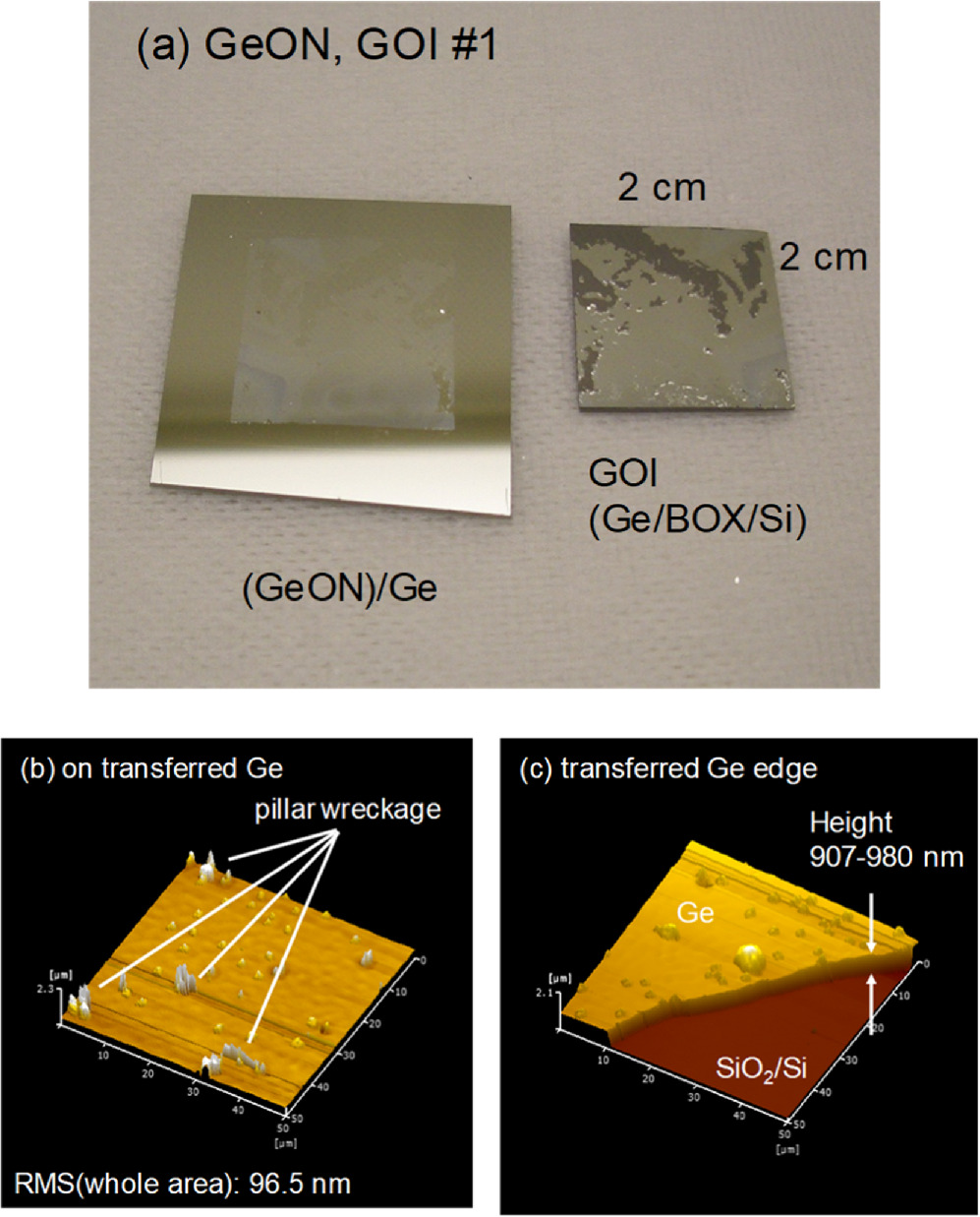
Fig. 4. (a) Fabricated GOI and remaining GeON after bonding and layer detachment. AFM images of GOI surfaces (b) at GOI center and (c) edge locations. No CMP was carried out.
Download figure:
Standard image High-resolution image3.2. PL spectra, Hall effect, and comparison with Smart-CutTM GOI
Figure 5 shows μ-PL spectra as measured on the fabricated GOI sample #1 evaluated at RT. For comparison, spectra measured on bulk Ge with a thickness of 500 μm are also plotted. PL spectra are taken at three different positions on the same GOI chip. PL peaks corresponding to direct bandgap transitions in Ge (0.80 eV) are clearly observed. PL signals from GOI have higher intensities than those obtained from the bulk Ge reference sample. This might be explained by carrier confinement in the thin GOI layer, 47) since the limited Ge thickness prevents exciton diffusion, and the probability of radiative recombination increases in the case of GOI compared with bulk Ge. In addition, the PL intensity caused by the indirect band-to-band transitions, at an energy around 0.7 eV, is significantly lower in case of the GOI sample.

Fig. 5. μ-PL spectra of GOI fabricated from GeON (sample #1) measured at three different positions of the same chip. The μ-PL spectrum as measured on bulk Ge result is shown as a reference.
Download figure:
Standard image High-resolution imageFigures 6(a) and 6(b) show the GOI thickness dependence of the hole mobility (μp) and the hole concentration (p) evaluated using Hall effect measurements for the GOI samples #1 and #2, respectively. The thickness dependence of μp and p is obtained by a cyclic repetition of Hall effect measurements, GOI thinning by wet-chemical etching in an H2O2-based solution. For both samples #1 and #2, an increase in μp together with a slight decrease in p with decreasing GOI thickness is observed. In particular, for a GOI thickness of 68 nm, μp and p of GOI sample #1 reach 670 cm2V–1s–1 and 6.8 × 1015 cm–3, respectively. These values are higher than those reported for GOI fabricated by direct wafer bonding and mechanical polishing. 28) The previous articles about GOI report that the carrier mobility degrades with decreasing GOI thickness in relatively thick (>50 nm) GOI cases. 28,48,49) This study based on GeON, however, indicates a different result. Although we still can not clarify the reason, one possible origin is the starting GeON contains the mobility (and other electrical features) distribution in the depth direction. Namely, the top of GeON, which will be the very bottom layer after bonding, may show the highest mobility. As a matter of fact, the secondary ion mass spectroscopy analysis of GeON shows a gradient of impurity concentration in the depth direction, particularly for the GeON seed layer. 21) We will continue further investigating this issue and the mobility behavior in the extremely thin (<10 nm) GOI region.
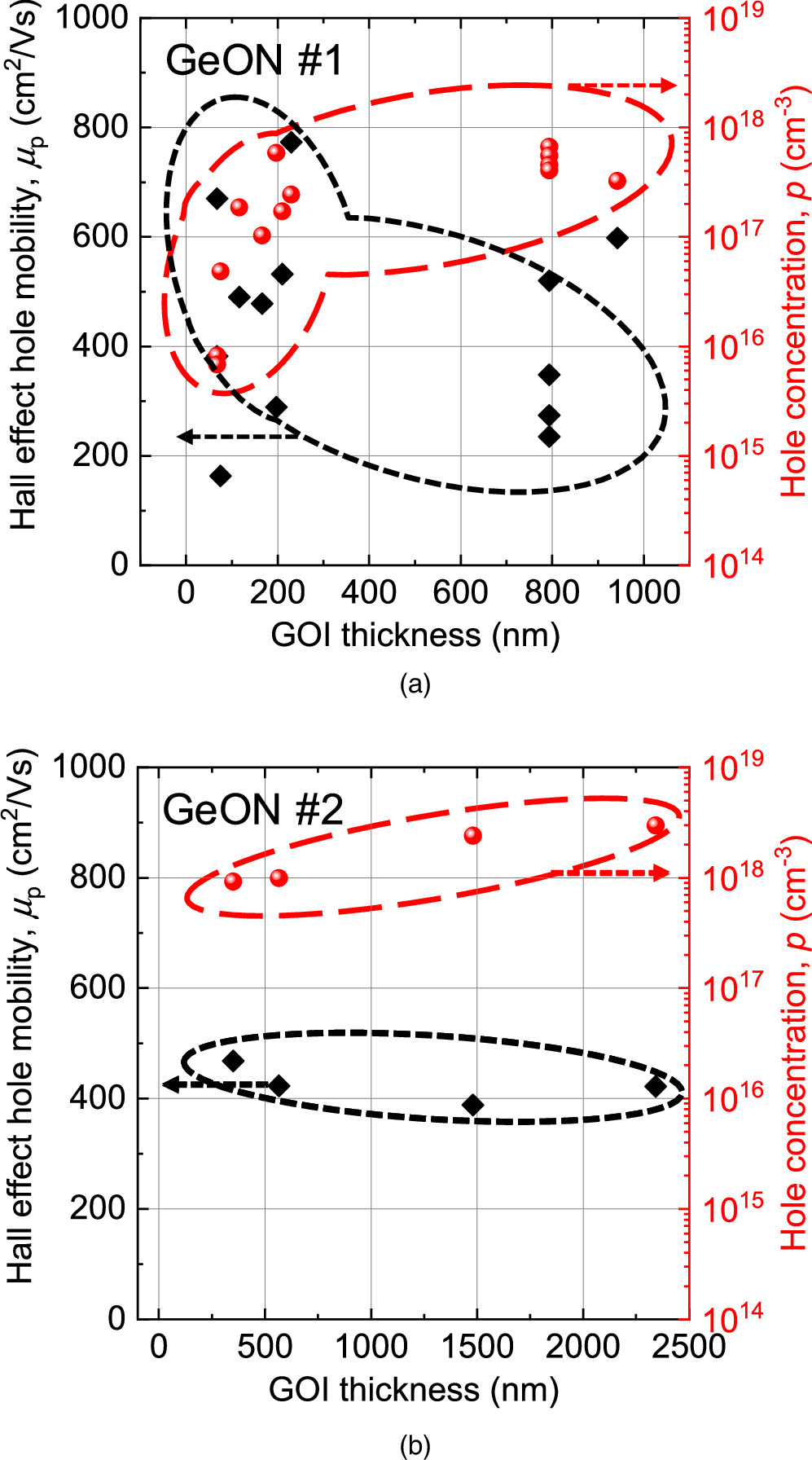
Fig. 6. μp and p dependence on GOI thickness. Original GeON are (a) GeON #1 and (b) GeON #2. Data have been obtained by cyclic GOI thinning and Hall measurements.
Download figure:
Standard image High-resolution imageNext, some characteristics of GOI based on the GeON template and Smart-CutTM methods are compared. Figure 7 presents μ-PL results from GOI fabricated by the Smart-CutTM method. 47) The signal intensity of the Smart-CutTM GOI is significantly lower compared to the μ-PL signals of GOI based on GeON and those of bulk Ge, previously shown in Fig. 5. It nevertheless needs to be mentioned that the GOI is thinner than the bulk Ge wafer. In addition, variations in the PL signal for different measurement positions are seen in Fig. 7, while they are drastically reduced in GOI based on GeON. Figure 8 compares the μp and p as measured for the GOI based on GeON (#1) and the Smart-CutTM GOI. 48) The first one shows a reduced degradation of μp and p with reducing Ge thickness in comparison to those obtained for the Smart-CutTM GOI. Although the thin (∼20 nm) Smart-CutTM GOI shows high μp, the p is also high which will be an obstacle for application. A TEM structural analysis was carried out to discuss the difference between GeON-based GOI and Smart-CutTM GOI in-depth. Figures 9(a) and 9(b) show the cross-section of the GeON-based GOI #1 and Smart-CutTM GOI, respectively. 33) The former one keeps a high crystallinity near the Ge/Al2O3 interface. On the other hand, the latter one contains a lot of defects displayed as black dots in the Ge crystal. These defects are introduced during hydrogen ion implantation before bonding and are hard to recover in the Ge case, different from the Si case. The defects may reflect differences between two GOIs in the PL and Hall effect results. In PL measurement, defects cause weak signal intensity and variation from the different positions. As for the Hall effect, defects cause an increase in carriers and a decrease in mobility. The comparison of electrical and optical material properties therefore suggests that the GOI fabricated from GeON has a better crystallinity than the Smart-CutTM GOI. However, fluctuations of the PL signal (Fig. 5), as well of μp, and p (not shown) still indicate some degree of non-uniformity in the GeON-based GOI. Improving the layer uniformity is one of the next challenging issues.

Fig. 7. μ-PL spectrum for the Smart-CutTM GOI as reported in our previous study. (Reproduced from Ref. 47 with permission. © IOP publishing, the Japan Society of Applied Physics).
Download figure:
Standard image High-resolution image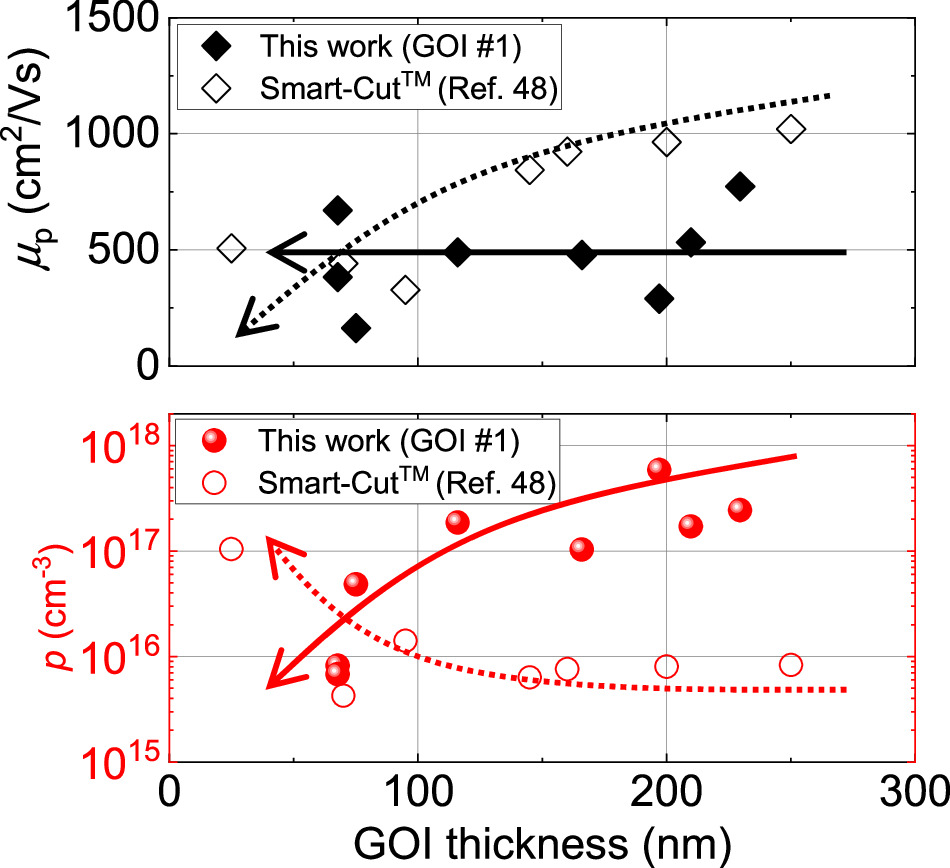
Fig. 8. Comparison of GOI thickness dependence of μp and p as measured for GOI samples fabricated in this study and GOI fabricated following the Smart-CutTM GOI. 48)
Download figure:
Standard image High-resolution image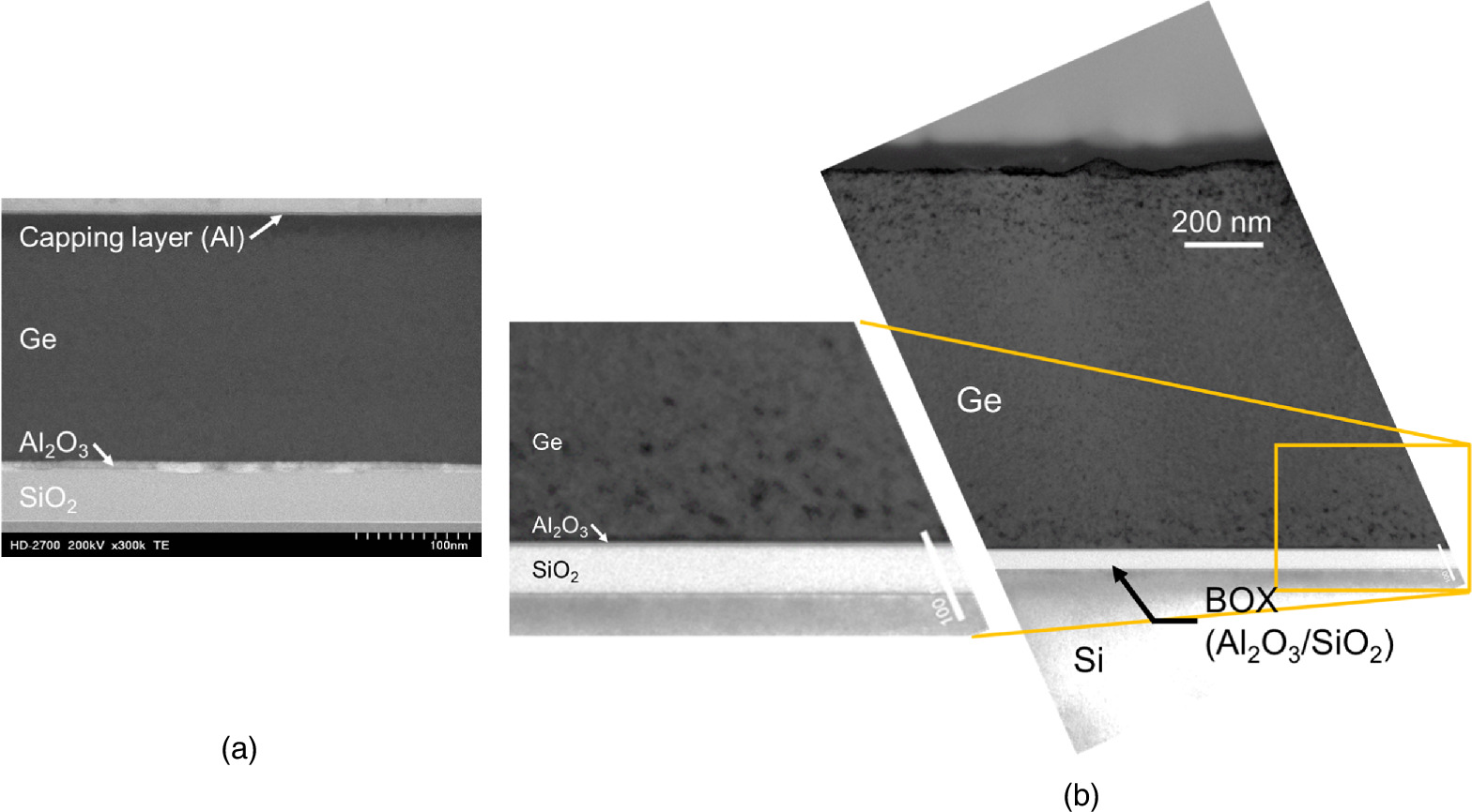
Fig. 9. Cross-sectional TEM images for (a) GOI made from GeON #1 and (b) made using Smart-CutTM method. [(b) is Reproducted from Ref. 33 with permission. © IOP publishing, The Electrochemical Society].
Download figure:
Standard image High-resolution image3.3. Electrical characterizations of back-gated GOI capacitors and MOSFETs
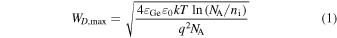
A back-gate GOI capacitor has been fabricated to characterize the quality of the GOI layer and of the Ge/BOX(Al2O3) interface. Figure 10(a) shows the capacitance–voltage (C–V) characteristics of the back-gate GOI capacitor built on GOI #2. The GOI thickness is 350 nm thick. For comparison, the theoretically calculated C–V curves of Si and Ge MOS capacitors are drawn, together with the corresponding structures and series-connected results of the Ge-insulator-Si capacitor. In the calculations, the same MOS dielectric thickness has been assumed as in the experiment, about 50 nm equivalent oxide thickness. The impurity concentration considered for Si corresponds to that of the Si substrate. For Ge, the hole density obtained by the Hall effect measurements [Fig. 6(b)] is assumed. Here, the maximum depletion layer width (WD,max), determined using the following equation, is 32 nm.
Here, εGe is the dielectric constant of Ge, ε0 is the permittivity of vacuum, k is the Boltzmann's constant, T is the absolution temperature, NA is the acceptor concentration, ni is the intrinsic carrier density of Ge, and q is the elementary charge. The GOI thickness of 350 nm is sufficiently thicker than WD,max, so we did not perform any special manipulations on the theoretically calculated C–V curve of the Ge-insulator-Si capacitor. Applying a voltage on the semiconductor-insulator-semiconductor capacitor structure with the same conduction type on both sides results in a carrier accumulation on one side and a depletion (or inverted) state at the other side of the structure, as shown in Fig. 10(b). As a result, the capacitance reaches the highest value at the voltage which gives exactly flat band profiles at both sides of the oxide. The experimental result nicely follows the theoretical calculation.
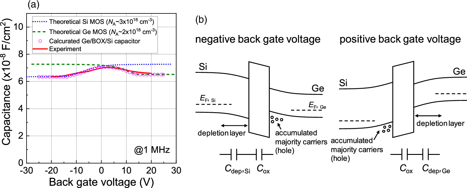
Fig. 10. (a) C–V characteristics of a GOI back-gate GOI capacitor made from GeON #2 together with theoretically calculated curves. (b) Band diagram schemes under negative (Ge accumulation) and positive (Ge depletion) gate voltages from the backside.
Download figure:
Standard image High-resolution imageBack-gate MOSFET devices have been fabricated for a further in-depth electrical characterization of the GOI. For the back-gate MOSFETs, the GOI thicknesses (tGOI) are lower than WD,max, as summarized in Table II. The fabricated MOSFETs therefore operate in the fully depleted mode. The drain current–drain voltage (ID–VG) characteristics for p- and n-MOSFET are shown in Figs. 11(a) and 11(b), respectively. Both viewgraphs show typical MOSFET output curves, illustrating that the GOI fabrication procedure starting from the GeON template can be appropriate to realize high-quality GOI and associated devices. Finally, Figs. 12(a) and 12(b) show the ID–gate voltage (ID–VG) characteristics for the accumulation mode p-MOSFET and inversion mode n-MOSFET, respectively. A clear on/off behavior can be seen for both n- and p-MOSFET devices. The n-MOSFET shows a large gate-induced drain leakage (GIDL) even at a low VD. It comes from minority carrier tunneling injection from the drain to the channel. Such large GIDL, even under low VD (<50 mV), are often observed in metal S/D MOSFETs and back-gate MOSFETs. 28,46,50) We calculated the interface trap density (Dit) of Ge/BOX interface from the subthreshold slope (SS) of the n-MOSFET. The SS at VD = 0.1 V and the corresponding Dit values are about 900 mV/decade and 2.8 × 1012 cm−2eV−1, respectively. Here, we used the SS and Dit model for fully depleted back-gate SOI MOSFET. 51) The obtained Dit value agrees well with the former study on the Al2O3/Ge stacked MOS capacitor. 52) The field-effect mobilities (μFE) have been calculated from a differential of ID–VG characteristics and BOX layer thickness. The calculated μFE's are 290 and 50 cm2V–1s–1 for p-MOSFET and n-MOSFET, respectively. Lim et al. reported p- and n-channel back-gate MOSFETs on Smart-CutTM GOI, respectively. 53,54) They also mentioned that hydrogen implantation damage for Smart-CutTM is the issue to improve GOI quality. Although it should be noted that the structure and thickness of the BOX layer and the thickness of the GOI layer are far from our study, our back-gate MOSFETs on GeON-based GOI show a higher on/off ratio with low operation VG. Therefore, the proposed GOI fabrication scheme has a high potential for producing high-quality GOI for advanced device fields.
Table II. Specifications of the back-gate MOSFETs in this study.
| MOSFET | p (cm−3) | WD,max (nm) | tGOI (nm) |
|---|---|---|---|
| p-MOSFET | 8.2 × 10¹⁵ | 252 | 67.7 |
| n-MOSFET | 1.0 × 10¹⁷ | 86.6 | 27.0 |
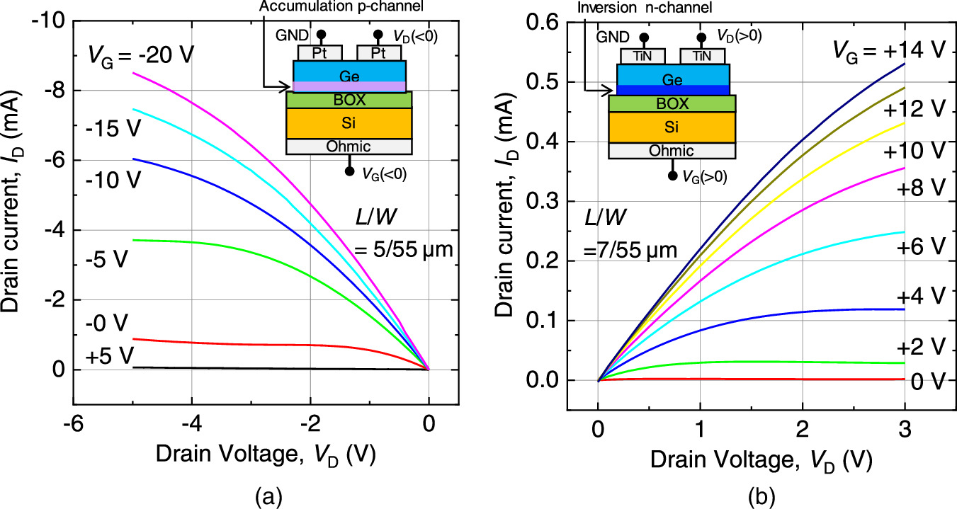
Fig. 11. ID–VD characteristics of the back-gate MOSFETs on the GOI from GeON #1. (a) Accumulation mode p-MOSFET. (b) Inversion mode n-MOSFET.
Download figure:
Standard image High-resolution image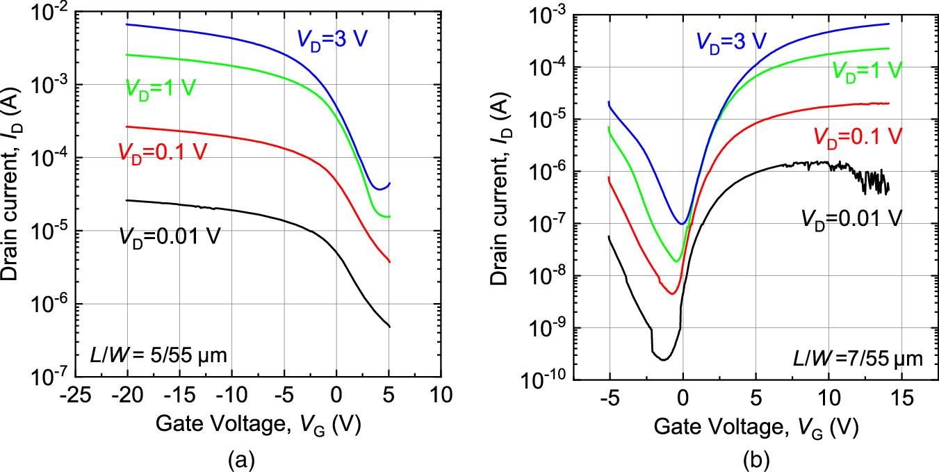
Fig. 12. ID–VG characteristics of the back-gate MOSFETs fabricated on GOI from GeON #1. (a) Accumulation mode p-MOSFET. (b) Inversion mode n-MOSFET.
Download figure:
Standard image High-resolution image
4. Conclusions
A novel GOI formation scheme based on direct wafer bonding starting from the GeON template is proposed. We report a successful wafer bonding and layer detachment, and compared its electrical/optical/structural characteristics with GOIs fabricated using other methods of mechanical thinning and Smart-CutTM. PL signals from GeON-based GOI are higher in intensity compared to those measured for bulk Ge which might be due to carrier confinement effects. The GeON-based GOI shows higher carrier mobility, in Hall effect characteristics than GOI fabricated by direct bonding and mechanical polishing even in the low Ge thickness region. These observations are correlated by TEM with a higher crystal quality at the interface of the Ge-oxide interface. The fabricated GeON-based GOI also shows a better uniformity than Smart-CutTM GOI. The electrical material properties are further illustrated by the characteristics of fabricated back-gate GOI capacitors and MOSFETs. The presented back-gate GOI capacitor follows the theoretically predicted C–V behavior. Moreover, functional back-gate MOSFETs with excellent operation curves are reported. The proposed fabrication scheme therefore enables the production of high-quality GOI for advanced devices in electronics, optics, spintronics, and quantum application fields.
Acknowledgments
This work was partially supported by a Grant-in-Aid for Scientific Research (No. 19H05616), JSPS-FWO Bilateral Joint Research Projects, and the Cooperative Research Project of the RIEC, Tohoku University. The development of the GeON template was carried out under a program of and funded by the European Space Agency (ESA) with contract no. 4000129924/20/NL/FE. The view expressed herein can in no way be taken to reflect the official opinion of the European Space Agency. The TEM analysis was conducted by Melco Semiconductor Engineering Corp.