
Abstract
Plasmonic color is a structural color generated via preferential light absorption and scattering in dielectric nanostructures. In this study, a large plasmonic color image was successfully fabricated by an electron beam lithography (EBL) system. A software program, referred to as P-color in this study, was developed to facilitate the conversion of a desired color bitmap image to a GDS file composed of multiple nano-patterns to realize plasmonic color. The relationship between the color, width, and pitch of the pattern structures was investigated under different area-dose conditions during EBL as basic data for plasmonic color image design. After establishing conversion techniques for both the large-capacity GDS and EBL files, a plasmonic color image sample with a size of 60 mm × 40 mm area (which is difficult to fabricate using a conventional point-type EBL system) was successfully fabricated.
Export citation and abstract BibTeX RIS
1. Introduction
In various fields, such as mobile electronic devices and automobiles, it is valuable to improve surface performance and value via the formation of nano-patterns. 1–3) At present, nanostructure colors based on biomimetic structural colors attract attention. For example, morpho-related single rare color 4,5) is used for luxury automobiles. However, resolution control and function of information transfer are under development.
Printing technology using ink can produce various colors, and inkjet printers are widely used across different fields. 6–9) Despite being a highly efficient printing technology, the impermanent durability of its ink and the lack of possible significant improvements in printing performance, such as resolution, are major drawbacks. Thus, there is increased demand for next-generation technology.
As a solution, we conducted research and developed a nano-processing technology that can provide nano-decoration with structural colors, such as complex photographs over a large area, with the aim of developing applications for nano-decoration, security, and other applications.
Plasmonic color is a structural color created by resonant interactions between light and metallic nanostructures without the use of dyes. Plasmonic structural coloring effects result from the resonant coupling of light with free electrons in metal nanoparticles, known as surface plasmons. 10–13) Theoretically, the size of one pixel can be on the nanoscale, rendering it possible to achieve extremely fine depictions compared to conventional printing technology. 14) The promising applications include decoration, security, optical components, and coatings. Several studies related to this technology have been conducted in Japan and overseas. 15–29) Recently, an efficient color printing method employing sub-micrometer-scale plasmonic pixels of a single constituent metal structure was demonstrated by Mudachathi and Tanaka. 15) They demonstrated high-quality color plasmonic images with sub-micron structures by a simple fabrication process. When we apply those ideas to various color images, electron beam lithography (EBL) is a prime candidate as it can easily produce any figures with such dimensions. From the viewpoint of nanostructure patterning, EBL is a good selection, however, the throughput of EBL, especially point-type EBL system is very slow. Therefore, the fabricated areas of plasmonic color images were limited to within 1 mm2 in most cases.
Since 2016, we have been developing ultra-high-speed electron beam (UHSEB) processing equipment, which is more than 100 times faster than conventional systems, achieving writing tasks that would require 100 days in just 24 h. 30) In addition, we have developed a combined use of nanoimprinting, which can form nanostructures on a wafer scale at a low cost, drastically boosting the throughput.
In this study, we attempted to establish the fabrication technology of low-cost, large-area nanostructured color substrate using an UHSEB lithography system. We adopted the same approach as Mudachathi and Tanaka 15) because of the simplicity of the fabrication process. As basic data for plasmonic color image design, the relationship among process parameters under different area dose conditions during EBL was investigated. Additionally, a software program (referred to as P-color), which facilitated the conversion of a desired bitmap image to a GDS file composed of several nano-patterns to realize plasmonic color, was developed. After establishing conversion techniques for both the large-capacity GDS and EBL files, a plasmonic color image sample with a size of 60 mm × 40 mm area was fabricated.
2. Experiments
Plasmonic color can adjust the color visible to the naked eye by controlling the wavelength of light absorbed by surface plasmons, depending on the pattern size, pitch, and height of the nanostructures, as well as the type of metal and dielectric. Figure 1 shows a schematic of a single plasmonic color element. The colors of the plasmonic color elements can be changed systematically by varying the square width W and inter-square gap G (Pitch P = W + G). As high-value decoration is considered one of the main application fields, we chose Ti as the metal layer material for the realization of color, mainly because of its high resistance to corrosion and excellent biocompatibility.
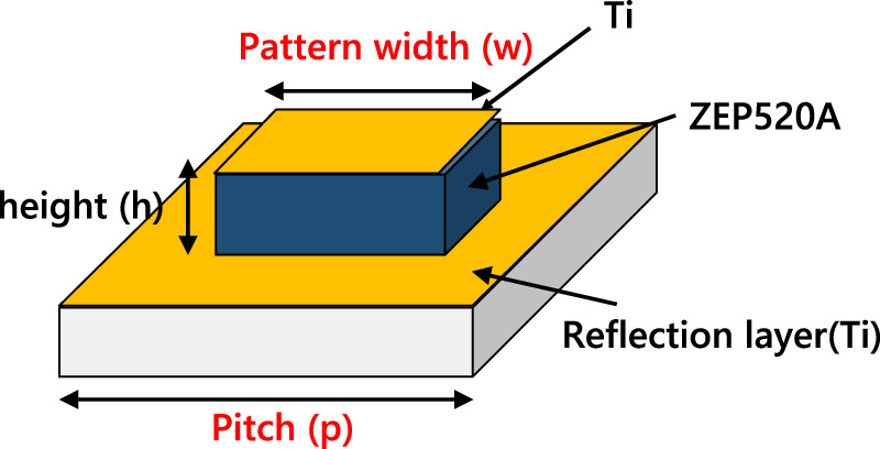
Fig. 1. Schematic drawing of a single plasmonic color element.
Download figure:
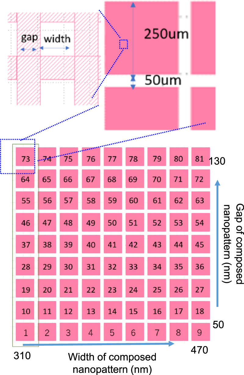
Standard image High-resolution imageThe process flow for fabricating the plasmonic color image samples is listed in Table I. The first step is to investigate the relationship between structural color and dimensions of pattern structure. For producing the best color forming, simulations should be done for the determination of plasmonic structures. However, we omitted simulations and adopted an easy way i.e. experimental exploration for appropriate plasmonic structures based on the manner of Mudachati and Tanaka. 15) We had carried out several preliminary experiments using various plasmonic structures and selected a promising structure as shown in Fig. 2, which yet showed not enough color forming at this moment. We focused on the structure (hereafter, we call it a color pallet) and investigated 16 different dose conditions to modify the width and gap of nano-patterns as 81 color variables for realizing better color forming.
Table I. Process flow of fabrication of plasmonic color image sample.
| Procedure | |
|---|---|
| Step 1 | Investigation of the relationship between structural color and dimensions of pattern structures (ex: width, pitch, etc.) |
| Step 2 | Transformation of original bitmap image file to GDS CAD file by using program software of P-color developed by AIST |
| Step 3 | Conversion of data format from.GDS to.car for EBL |
| Step 4 | EBL using UHSEB |
| Step 5 | Sputtering metal (Ti) |

Fig. 2. Design of drawing to investigate the relationship between the pattern dimensional factors and colors.
Download figure:
Standard image High-resolution imageAfter investigating the relationship between structural color and dimensions of pattern structures, an original color bitmap image is transformed into a colorless CAD file. For this transformation, the program software "P-color" that we have developed was used. In the next step, GenISys Beamer software was used to convert the CAD file (GDSII format) into an EB drawing file (CAR format). A proximity-effect correction was also performed.
EBL experiments were performed using a 50 kV UHSEB system developed by a commercial company (Elionix Inc.) and our institute (AIST). The UHSEB allowed for a beam current of 1 μA and a large field size of 10 mm × 10 mm; thus, it had a throughput 100 times higher than that of conventional point-beam-type EB systems. The major specifications of the UHSEB are summarized in Table II. In preliminary research, the line width of 100 nm could be achieved at 3 nA (50 kV, 10 mm × 10 mm). In this study, beam current was set at 3 nA considering stability and distribution uniformity of pattern dimensions. Electron beam resists ZEP520A (Nippon Zeon Co.) were spun onto a silicon wafer by spin-coating with thicknesses of 100 nm. The films were then baked on a hot plate at 90 °C for 3 min. After EBL, the samples were developed in O-xylene for 1 min. The remaining resist patterns act as dielectric as shown in Fig. 1. Subsequently, Ti was deposited onto the sample surfaces with a thickness of 50 mm.
Table II. Main specification of UHSEB.
| Issues | Specification |
|---|---|
| Maximum acceleration voltage | 50 kV |
| Beam current | Maximum 1 uA (effective current: 100 times higher than that of conventional EB system) |
| Beam deflection area | Maximum 10 mm square (100 times larger than that of conventional EB system) |
| Deflection signal clock frequency field size | 400 MHz. (4 times higher than that of the conventional EB system) |
| Minimum pattern width to be made | 100 nm |
We investigated the color changes of the plasmonic color elements array (1 pixel size: 250 μm × 250 μm) comprising metal/resist squares with different widths (range of 310–470 nm) and gaps (range of 50–130 nm) as illustrated in Fig. 2.
For the large capacity conversion (60 mm × 40 mm) from bitmap images to GDS and CAD files using P-color software, data errors were removed via the addition of several solutions (e.g., functions for group conversion of color data, pattern grouping, and parallel computing) developed in this study.
3. Results and discussion
3.1. Plasmonic color design
Figure 3 shows the photograph of the 4 × 4 arrays of color pallets on the surface of a 4 inch Ti/resist/Si sample fabricated under different area dose conditions (90–240 μC cm−2). Different colors are observed at different dose conditions. We can see several colors in a pallet by the naked eye and similar pallets are fabricated in these dose conditions.
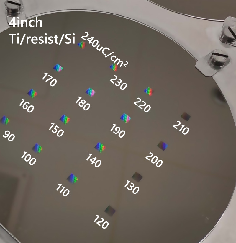
Fig. 3. Photo of a Ti/resist/Si sample surface.
Download figure:
Standard image High-resolution imageFigure 4 shows an example of a color pallet obtained for the dose condition of 170 μC cm−2. The color information of each plasmonic color pixel was obtained using an Olympus STM7. Relatively clear 81 colors are obtained in this pallet.
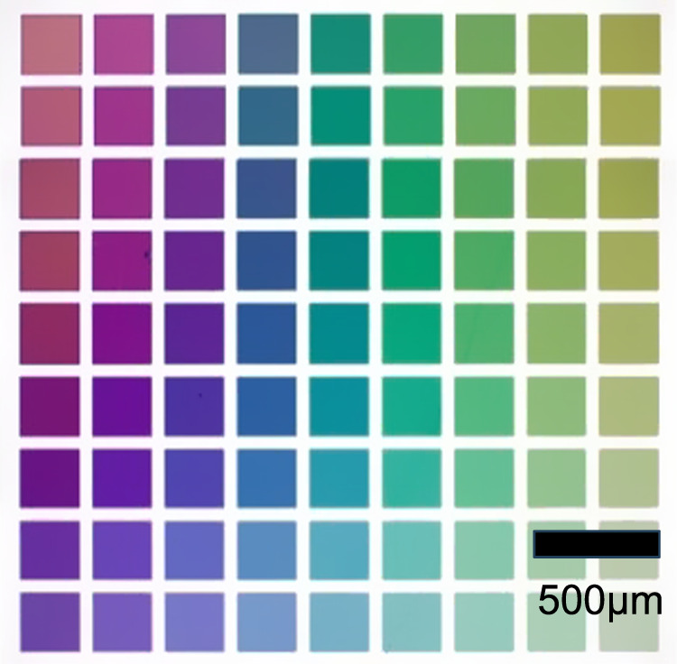
Fig. 4. Optical microscope image of an example of chip area for 170 μC cm−2.
Download figure:
Standard image High-resolution imageFigure 5 shows SEM images of patterns with two different colors (violet and yellow) elements (No. 1 and No. 62 positions shown in Fig. 2,) in the pallet.
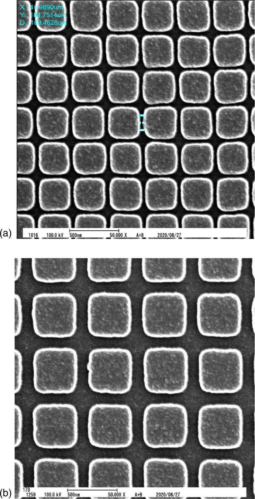
Fig. 5. SEM observation examples in the patterned area for 170 μC cm−2.
Download figure:
Standard image High-resolution imageAs can be expected, the change in dose conditions must change the pattern dimensions and induce a difference in color by tuning dimensions such as width and gap. For example, the pattern gap as a function of area dose for the minimum feature size (50 nm gap and 310 nm width pattern) in Fig. 6. It was observed that the pattern gap increased with the increase of areal dose. Gaps become approximately 10 nm wider with a 20 μC cm−2 increase in area dose. Under the condition of 170 uC cm−2, the gab measured has good agreement with the designed value (50 nm gap and 310 nm width)
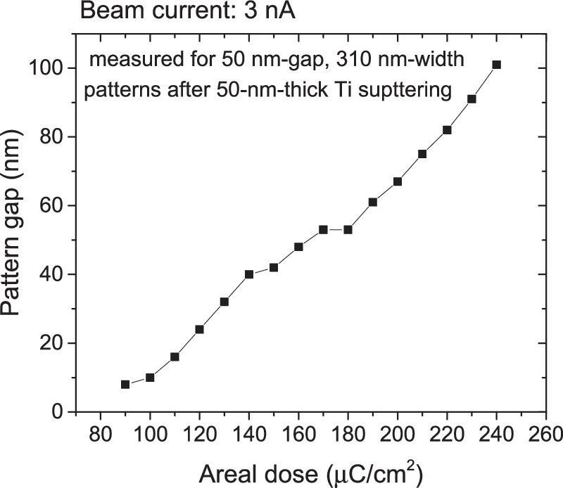
Fig. 6. Relationship between pattern gap and areal dose for plasmonic elements with 50 nm gap and 310 nm width.
Download figure:
Standard image High-resolution imageFigure 7 shows color pallets with different doses. Sixteen palates (each pallet has 81 colors) were obtained, and some of them are shown. With increasing aria dose, the colors shifted in the down-right direction owing to dimensional changes in the plasmonic color elements. The aim of this study is to convert a colorful image into 81 plasmonic colors reflecting the original color. Thus, colors contained in a color pallet should be various hues with good saturation. From the viewpoint of usefulness, the color pallet for 170 uC cm−1 looks good and the judgment is supported by the result shown in Fig. 6.

Fig. 7. Colormaps with the different doses.
Download figure:
Standard image High-resolution imageIn this case, we think our selection may be the best, however, someone might select another color pallet among the similar pallets. For good selection, it is useful if there exists a figure of merit (FOM) that characterizes the performance of the color pallet. Besides RGB, we have different ways to express colors, e.g. HSV and CMYK, and we thought that HSV in particular would be a good indicator because it matches human sensibilities. As an index for quantifying the quality of the image, we focus saturation of the HSV color model. When a color consists of (R, G, B), Saturation (S) is determined by the following formula,

where MAX and MIN are maximum and minimum function, respectively.
Figure 8 shows a conversion of a color pallet to a saturation map. Each color element is converted to a monochrome saturation element. Here, we define the FOM of a pallet by the averaged saturation of the color pallet.
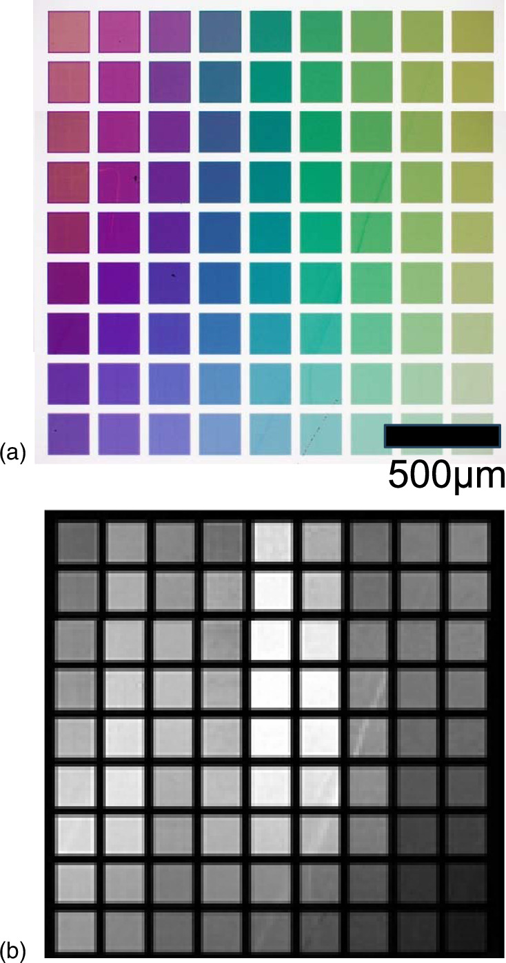
Fig. 8. Calculation of R G B compositions: (a) color palate sample and (b) saturation of HSV.
Download figure:
Standard image High-resolution imageFigure 9 shows the relationship between dose and averaged saturation. As expected, the average saturation of HSV is highest for the sample fabricated under 170 μC cm−2. We can select the best pallet among similar pallets without resorting to sensory testing. This method is equally applicable and useful when increasing the number of colors in a palette.
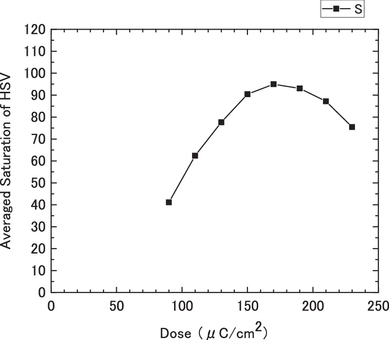
Fig. 9. Relationship between dose and averaged saturation.
Download figure:
Standard image High-resolution image3.2. Conversion of colors to figures of plasmonic device
As previously listed in Table II, the first step in the process was to transform the original bitmap image into a GDS file composed of nano-patterns to realize a plasmonic color. For this, we developed a software program (P-color) that enabled us to convert a desired bitmap image to a GDS file composed of several nano-patterns to realize plasmonic color. The major functions of the P-color software are listed in Table III. Following this procedure, the pattern was converted from CAD data (GDS format) to EBL data (CAR format for EBL system made by Elionix Inc.) using EBL software BEAMER (GenISys GmbH).
Table III. Major functions of P-color software.
| Technical issues | Functions |
|---|---|
| Transformation of the plasmonic nano-pattern image from a bitmap image to a CAD file | Division of bitmap image by input pixel size |
| Equalization of RGB colors around positions to pick up RGB information. | |
| Generation of nano-patterns based on the data related to the relationship between the color and | |
| Conversion from GDSTXT to GDSII format | |
| Handling of large-capacity GDS files | Group conversion of color data |
| Pattern grouping | |
| Parallel computing |
Figure 10 shows an example of BMP to GDS conversion using P-color software. The original image shown in Fig. 10(a) is converted to an image consisting of 81 colors. One of the converted 81 color images is shown in Fig. 10(b). The bright part is the pattern data consisting of plasmonic device figures corresponding to a selected color. P-color software generates GDS data of 81 layers likewise. In some cases, the GDS data consisting of numerous plasmonic device patterns are so huge that we had to reduce the resolution of converted images or split an original image into a few hundred tiles for the following BEAMER data conversion.
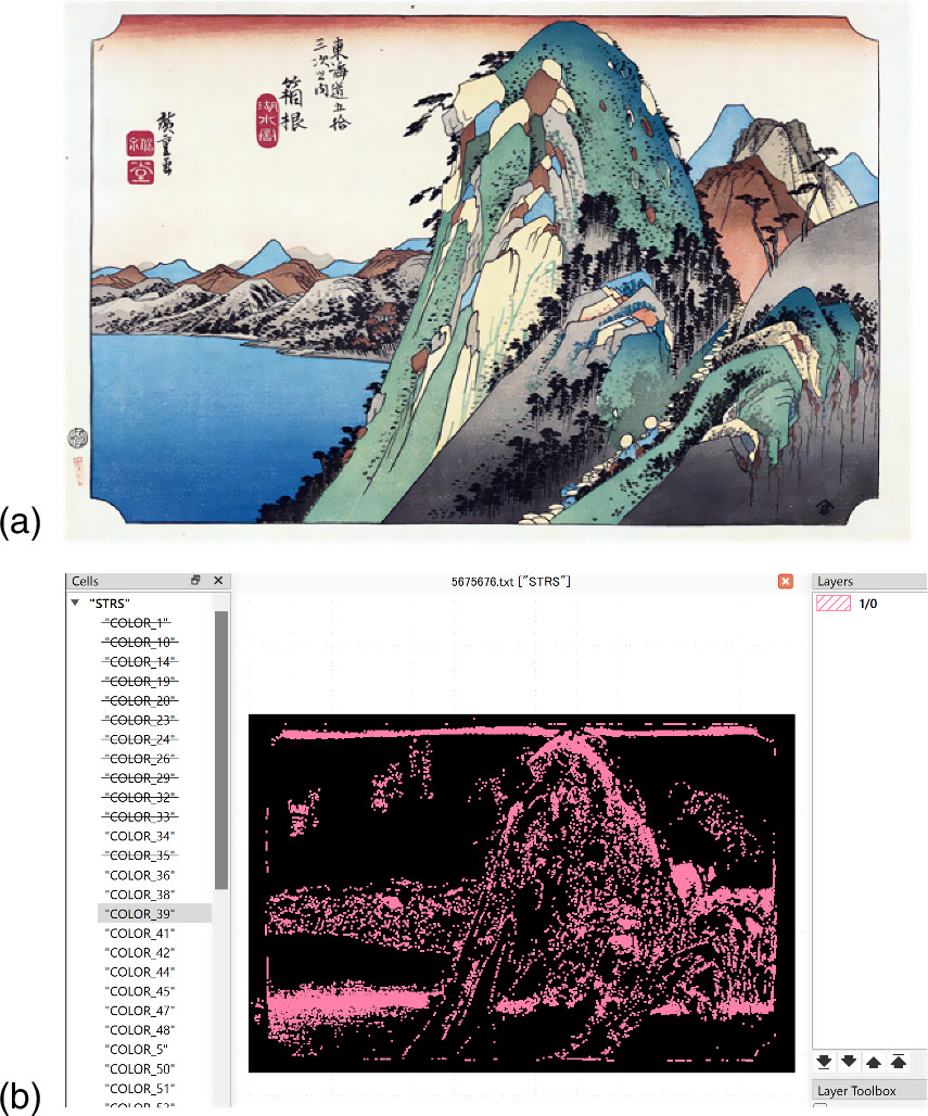
Fig. 10. Example of BMP to GDS conversion: (a) original bitmap image for conversion and (b) a layer in converted GDSII file having different layers according to colors.
Download figure:
Standard image High-resolution image3.3. Validity of process and fabrication of large plasmonic color image
Figure 11(a) shows plasmonic color images on a 4 inch Si wafer fabricated by the aforementioned process and Fig. 11(b) shows a magnified image with an optical microscope. Plasmonic color samples with the size of 6 mm × 4 mm were successfully obtained. In previous literature, 1–5) in most cases, the size of the plasmonic color samples fabricated using EB was less than 1 mm square, so the size obtained here is considerably larger than those previously reported. We should note that the exposure time of the plasmonic images is within 1 h, thanks to the ultra-high throughput of the UHSEB system. As previously mentioned, the data volume is a cumbersome issue. So, to reduce the file capacity for the conversion of format, we utilize the group conversion function. In the method, by setting the minimum pixel size to 10 μm, pixels within 10 μm2 can be converted as one group, thus facilitating a remarkable reduction in the calculation amount.
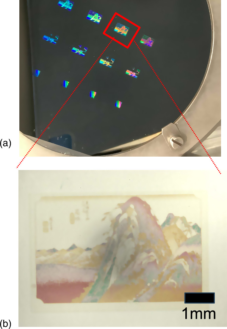
Fig. 11. Plasmonic color structuring on 6 mm × 4 mm squares: (a) 4 inch wafer after EBL and Ti sputtering and (b) magnified optical microscope image of an area.
Download figure:
Standard image High-resolution imageIn the next step, we attempted to fabricate a plasmonic color image with dimensions of 60 mm × 40 mm. This is an enormous and valuable challenge because the exposed area is 100 times larger than in our previous case and the plasmonic color image can be seen by the naked eye without using microscopes if successful. The pixel size was set at 10 μm, and the number of polygons was estimated at approximately 240,000,000,000. In this EB exposure, the drawing area exceeds the EB's unit exposure field by several tens of mm2, thus the drawing area was split into 12 × 8 tiles. In each tile, innumerable nano-patterns in the size range of 80–800 nm must be arranged in a complicated manner according to the image or photograph. Therefore, the capacity of the drawing file to be generated is very large. In the early stages of development, errors often occurred when converting to drawing data because the capacity of the CAD data was excessively large. Thus, by tiling the EB area by 2.5 mm (Fig. 12), 384 (24 × 16) area patterns were generated. Figure 11 shows the EB resist image after resist development. The elapsed time for EB drawing was 192 h. We can see an uncolorful rectangular on a 4 inch Si wafer because metal sputtering was not performed.
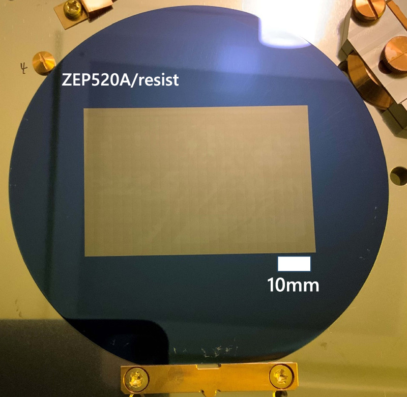
Fig. 12. The surface of the sample after EBL on a 60 mm × 40 mm area.
Download figure:
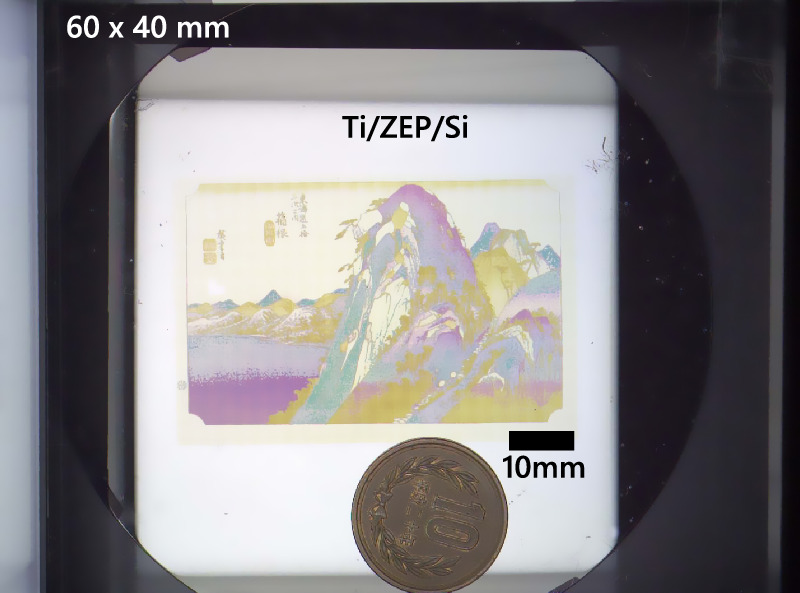
Standard image High-resolution imageFigure 13 shows an optical image of the plasmonic color image on the Ti/ZEP520A/Si wafer sample. The observation was performed with a camera using coaxial illumination. Plasmonic colors were successfully fabricated on a 60 mm × 40 mm area.
Fig. 13. Optical microscope image of the plasmonic color image on Ti/ZEP520A/Si wafer sample.
Download figure:
Standard image High-resolution image
4. Conclusion
A large plasmonic color image was successfully fabricated. First, we investigated the basic data for plasmonic color design. Subsequently, we developed a software program (P-color) that enabled us to convert a desired bitmap image to a GDS file composed of nano-patterns to realize plasmonic color. After establishing conversion techniques for both the large-capacity GDS and EBL files, a plasmonic color image sample with a size of 60 mm × 40 mm area (which is difficult to fabricate using a conventional point-type EB system) was fabricated. It is expected that much higher throughput can be accomplished compared to the process developed in this study by utilizing nanoimprint technology.
Acknowledgments
We would like to thank Mr. Komatsuzaki Tamao who provided us technical support for the development of the P-color program.