
Abstract
Benefitted from progress on the large-diameter Ga2O3 wafers and Ga2O3 processing techniques, the Ga2O3 power device technology has witnessed fast advances toward power electronics applications. Recently, reports on large-area (ampere-class) Ga2O3 power devices have emerged globally, and the scope of these works have gone well beyond the bare-die device demonstration into the device packaging, circuit testing, and ruggedness evaluation. These results have placed Ga2O3 in a unique position as the only ultra-wide bandgap semiconductor reaching these indispensable milestones for power device development. This paper presents a timely review on the state-of-the-art of the ampere-class Ga2O3 power devices (current up to >100 A and voltage up to >2000 V), including their static electrical performance, switching characteristics, packaging and thermal management, and the overcurrent/overvoltage ruggedness and reliability. Exciting research opportunities and critical technological gaps are also discussed.
Export citation and abstract BibTeX RIS

Content from this work may be used under the terms of the Creative Commons Attribution 4.0 license. Any further distribution of this work must maintain attribution to the author(s) and the title of the work, journal citation and DOI.
1. . Introduction
Power semiconductor devices are key to delivering high-efficiency energy conversion in power electronics applications such as electric vehicles, data centers, electric grids, renewable energy processing, and consumer electronics. 1) The market size of power semiconductor devices has reached $40 billion and is fast growing. 1,2) The advances in power devices hinge on innovations in semiconductor materials and device architectures. From the material perspective, power devices based on silicon (Si), silicon carbide (SiC), and gallium nitride (GaN) have been commercialized. 2,3) Several emerging materials with bandgaps larger than SiC and GaN, i.e. ultra-wide bandgap (UWBG) semiconductors, are being extensively researched, including gallium oxide (Ga2O3), aluminum nitride, aluminum gallium nitride, diamond, and boron nitride. 4)
Among these UWBG materials, Ga2O3 has shown particular promise as the Ga2O3 device technology has recently achieved several critical milestones for power applications. Power devices are used as solid-state switches to modulate considerable power flow in applications. Despite the wide range of specifications, industrial power devices are all packaged; they usually can conduct at least several amperes of current in the on-state, block at least tens or hundreds of volts in the off-state, and switch at a frequency of at least tens of kilohertz. During these operations, the junction temperature has to maintain below a safety limit (e.g. 150 °C–175 °C). In addition, power devices are required to possess good robustness against fault events (e.g. overvoltage, overcurrent, and surge energy 5)). These requirements define critical development milestones for any power device technology, i.e. the demonstration of (1) ampere-class devices with decent breakdown voltage (Vbr), (2) packaging and thermal management, (3) switching operation in converter applications, and (4) reliability and robustness.
Ga2O3 is featured by a high critical electric-field (projected to be up to 8 MV cm−1), controllable n-type doping with shallow dopants (1014 ∼ 1020 cm−3), and the availability of large-diameter wafers by the melt growth. 6–10) Low-cost beta-phase gallium oxide (β-Ga2O3) wafers have recently reached the 4-inch commercial milestone and are on track for the 6-inch wafer scale production by 2027. 11) This has paved the road for developing ampere-class devices. Since the first report of Ga2O3 transistors by Higashiwaki et al. in 2012–2013, 12,13) Ga2O3 power devices have witnessed fast progress not only in the innovation of device architectures but also in the scaling of power levels. Recently, large-area Ga2O3 power devices with a current of up to 135 A 14) or Vbr of up to over 2000 V 15) have been demonstrated. Beyond the die-level, packaging has been applied to large-area Ga2O3 devices and enabled a junction-to-case thermal resistance down to 0.5 °C W−1. 16) Excellent switching characteristics such as fast switching speed 17,18) and minimal reverse recovery 19) have been achieved in power converters. Impressive surge-current 20) and overvoltage ruggedness 15) have been reported in large-area Ga2O3 devices.
To the best of our knowledge, Ga2O3 is the only UWBG material that has made the above critical milestones for power applications. This suggests that the commercialization and application of Ga2O3 power devices are within reach. This prospect is well supported by the development of a reference power device technology slightly ahead of Ga2O3, the vertical GaN technology. Its development shows a similar trajectory from small-area devices to large-area diodes 21,22) and transistors 23–28) fabricated on large-diameter wafers. After a further breakthrough in avalanche 29–32) and short-circuit robustness, 33–35) vertical GaN devices rapidly evolve into industrial manufacturing and start to be deployed in various power applications. 36)
This article presents a timely review of the recent progress on large-area Ga2O3 power devices, with the scope covering their electrical performance, packaging and thermal management, converter operations, as well as robustness. This review also assists in identifying the gaps and immediate research needs. To date, despite several review papers on Ga2O3 devices, 7,37) such a review on the application prospects is lacking for Ga2O3 power devices. The literature is vast, and space is limited. For a tight focus, only ampere-class Ga2O3 power devices with a conduction current over 1 A are discussed in this paper.
This article is organized as follows. Section 2 discusses the static performance of large-area Ga2O3 devices. Section 3 presents their packaging and thermal management. Sections 4 and 5 discuss their switching characteristics in power converters and circuit-level robustness, respectively. Section 6 identifies the immediate research needs and concludes the paper.
2. . Electrical performance
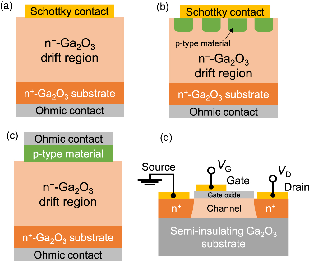
Currently, the reported ampere-class Ga2O3 rectifiers all deploy the vertical architecture with various junction structures including the Schottky barrier diodes (SBD), junction barrier Schottky (JBS) diodes, and p-n heterojunction diodes (HJD). As compared to the conventional p-n diode, the HJD relies on the p-n junction formed by n-type Ga2O3 and a distinct p-type material. The progress of these vertical Ga2O3 rectifiers is fast, and various edge termination designs have been reported to achieve high Vbr. For transistors, the only ampere-class Ga2O3 power transistor reported in the literature is the lateral Ga2O3 MOSFET with a saturation current over 2.5 A and Vbr over 400 V. 17,18) Schematics of the Ga2O3 vertical SBD, JBS diode and HJD, as well as lateral MOSFET, are shown in Fig. 1.

Fig. 1. (Color online) The schematic diagram of Ga2O3-based vertical (a) SBD, (b) JBS diode, (c) HJD, and (d) lateral MOSFET device.
Download figure:
Standard image High-resolution imageFigures 2(a)–2(c) benchmark the forward current versus Vbr, the forward current versus the differential specific on-resistance (Ron,sp), and the Ron ,sp versus Vbr of these ampere-class Ga2O3 power rectifiers and transistors. 14,15,17,19,20,38–49) A more complete set of performance parameters of the representative devices are summarized in Table I. For power diodes, the forward current is extracted at a forward voltage (VF) equal to 1.5 V higher than the turn-on voltage (Von); Ron,sp is the differential resistance after the diode is fully turned on. It is observed that both Vbr and Ron,sp show a decreasing trend as the forward current increases. This suggests that the non-uniformity in material properties and fabrication process, as well as a considerable defect density, are still the dominant performance limiting factors of Vbr in large-area Ga2O3 devices. On the other hand, the smaller Ron,sp achieved at high current levels is a positive sign that implies the superior conduction capability in large-area devices.

Fig. 2. (Color online) Benchmark of (a) forward current versus Vbr, (b) forward current versus Ron,sp, and (c) Vbr versus Ron,sp for the reported ampere-class vertical β-Ga2O3-based SBD, 14,20,38,42–48) JBS diode, 39,41,49) HJD, 15,19,40) and lateral MOSFET. 17)
Download figure:
Standard image High-resolution imageTable I. Summary of the key performance parameters of large-area β-Ga2O3 power devices.
| Device | References | Active area (mm2) | Current at VF = Von + 1.5 V (A) | Differential Ron,sp (mΩ·cm2) | Vbr (V) | Surge current (A) | trr (ns) | Converter tests and efficiency | |
|---|---|---|---|---|---|---|---|---|---|
| SBD | Normal | 14 | 115 | 44 | — | 240 | — | — | — |
| 19 | 1 | 2.6 | 5.8 | 350 | — | — | — | ||
| 9 | 11.7 | 10.35 | 117 | 38 | 11 | — | |||
| FP-SBD | 38,46,47 | 1 | 0.9 | 15.8 | 650 | — | 30 | — | |
| 1.44 | 0.85 | 22 | 760 | — | — | — | |||
| 9 | 15 | 12 | 240 | — | — | — | |||
| 45 | 1.8 | 1.8 | 60 | 300 | — | — | — | ||
| 2.6 | 2.6 | 77.3 | 261 | — | — | — | |||
| 20 | 9 | 16.3 | 6.75 | 700 | 68 | — | — | ||
| 48 | 9 | 30 | 5.13 | 378 | 59 | 98.9% b) | |||
| FP-MOSSBD | 42,44 | 2.89 | 2.8 | 17.1 | 1200 | — | — | — | |
| 16.81 | 8 | 34.9 | 948 | — | — | — | |||
| NiO JTE-SBD | 43 | 0.78 | 2.1 | 4.68 | 1300 | — | — | — | |
| JBS | Normal | 49 | 1 | 1.8 | 7.6 | 700 | — | — | — |
| FP-JBS | 41 | 9 | 10 | 11 | 550 | ||||
| 16 | 15 | 15 | 500 | — | — | — | |||
| Beveled FP-JBS | 39 | 9 | 5.1 | 13.5 | 1060 | 26.8 | 86.07% b) | ||
| HJD | Normal | 19 | 1 | 1.1 | 2.6 | 1370 | — | — | — |
| 9 | 9.1 | 5.85 | 462 | 45 | 11 | — | |||
| Beveled-mesa HJD | 15,40 | 1 | 1.5 | 2.26 | 2040 | — | 16.4 | — | |
| 1 | 1.2 | 1.9 | 1950 | — | — | 98.5% b) | |||
| Lateral MOSFET | 17 | 0.07 | 2.4 a) | 3.29 | 400 | — | — | DPT |
a)Saturation drain current. b)Power-conversion efficiency tested by PFC circuit.
For the trade-off between the differential Ron,sp and Vbr in Ga2O3 unipolar rectifiers, the Ga2O3 HJDs generally outperform the SBD counterparts, with some devices approaching the unipolar limit of SiC devices. This superior trade-off between the differential Ron,sp and Vbr does not necessarily lead to a superior trade-off between the conduction and switching loss, as the turn-on voltage of the HJD devices (2–2.5 V) is usually 1–1.5 V larger than that of SBDs and JBS diodes. 50,51) On the other hand, the SBDs and JBS didoes show the inferior Vbr with nearly no large-area devices exceeding 600 V. These comparisons reflect the pros and cons of using p-n junction in power diodes. Developing more advanced devices is necessary to simultaneously deliver the forward characteristics of SBDs and the reverse blocking capability of HJDs.
It is also interesting to scrutinize the max junction E-field (Emax) in these devices at their Vbr, which may suggest if the high critical E-field (EC) in Ga2O3 has been exploited in large-area devices. Here Emax can be calculated from the 1-D Poisson equations for the non-punch-through (NPT) and punch-through (PT) designs, 52,53) which represents the average junction field


where WD and ND are the thickness and net donor concentration of the drift region, respectively, q and ε0 are electronic charge and permittivity of vacuum, respectively, εn = 12.4 is the dielectric constant of β-Ga2O3 with the orientation of (001). 6,54,55)
Figure 3(a) shows the Vbr versus the calculated Emax for the reported large-area vertical Ga2O3 rectifiers. Most of the reported Ga2O3 SBDs and JBS diodes show an Emax below 3 MV cm−1, which is below the EC of GaN and SiC as well as the Emax of the state-of-the-art GaN/SiC devices. A few Ga2O3 HJDs show an Emax above 3.4 MV cm−1, suggesting the promise of the Ga2O3/NiO heterojunction junction to exceed the blocking field limit of GaN/SiC devices. Figure 3(b) plots the Vbr as a function of Emax 2 for large-area Ga2O3 diodes reported so far. The data points are found to roughly align with a linear relation with a slope of (5.5 ± 0.5)×109 V cm−2, suggesting that most large-area devices (even with the PT design) have not significantly surpassed the NPT limit. Interestingly, this slope agrees with the calculated 2qND/εn ε0 = 5.8 × 10⁹ V cm−2 with an ND ∼ 2 × 1016 cm−3, which is consistent with the usual epitaxy from the commercial vendor Novel Crystal Technology.
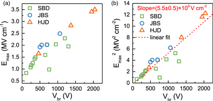
Fig. 3. (Color online) Benchmark of (a) Vbr versus Emax, and (b) Vbr versus Emax 2 for large-sized Ampere-class vertical β-Ga2O3-based SBD, 14,20,38,42–48) JBS diode, 39,41,49) and HJD. 15,19,40)
Download figure:
Standard image High-resolution imageAmong the ampere-class Ga2O3 diodes, the highest Vbr is 2040 V, which is obtained in the beveled-mesa NiO/Ga2O3 HJD reported by Zhou et al. 40) This device has a large on-state current of 20 A at ∼10.5 V (1.5 A at VF = Von + 1.5 V) and also exhibits the lowest Ron,sp of 2.26 mΩ·cm2 with a record Baliga's figure-of-merit of 1.84 (2.87) GW·cm−2 from DC (pulse) measurements. On the other hand, the highest current demonstrated in vertical Ga2O3 diodes exceeds 100 A. Ribhu et al. 14) reported the 115 mm2 vertical Ga2O3 SBD with the highest on-state current of 135 A at 6 V (44 A at VF = Von + 1.5 V) with a relatively low Vbr of around 240 V.
The JBS diodes hold the potential to combine the SBD's advantage of low turn-on voltage and the HJD's advantage of the enhanced reverse blocking capability. To date, p-NiO is a favorable p-type material for the HJD. Wu et al. 39) have fabricated 9 mm2 beveled field-plate (FP) JBS diodes, showing the largest Vbr of 1060 V with the forward current of 5.1 A at VF = Von + 1.5 V. Wei et al. 41) have reported a novel FP vertical Ga2O3 JBS diode with periodically distributed NiO/Ga2O3 heterojunction. The large-area 9 mm2 (16 mm2) devices exhibit the largest forward current of 37 A (51 A) at 6 V and 10 A (15 A) at VF = Von + 1.5 V, the Ron,sp of 11 mΩ·cm2 (15 mΩ·cm2), and Vbr of 550 V (500 V). Even though, the reverse leakage current level in JBS diodes is still much higher than that of the HJDs, especially under low reverse bias. Thus, advanced designs are needed to further improve the electrical performance of JBS diodes.
3. . Thermal management and packaging
For Ga2O3 power devices, an inevitable by-product of the superior electrical performance is the need to dissipate a higher density of heat due to the smaller device area. In addition, the concurrence of high current density and E-field could produce very high local heat flux, leading to non-uniform temperature distributions and local thermal runaway. What makes heat dissipation more challenging is the low thermal conductivity (kT) of Ga2O3, i.e. 11–27 W m−1·K−1. 56,57) To address these challenges, thermal management at both the device and package levels is essential. 58) At the device-level, substrate thinning and hetero-integration with high-kT substrates, such as SiC and diamond, have been reported. 59–62) Improved device characteristics up to 230 °C were demonstrated in Ga2O3 devices on SiC. 60) At the packaging level, junction- and double-side heat extraction with advanced cooling are essential for Ga2O3 devices. 63,64) Regardless of these thermal management approaches, their effectiveness has to be evaluated in packaged, large-area power devices as characterized by indispensable datasheet parameters such as the junction-to-case thermal resistance (RθJC).
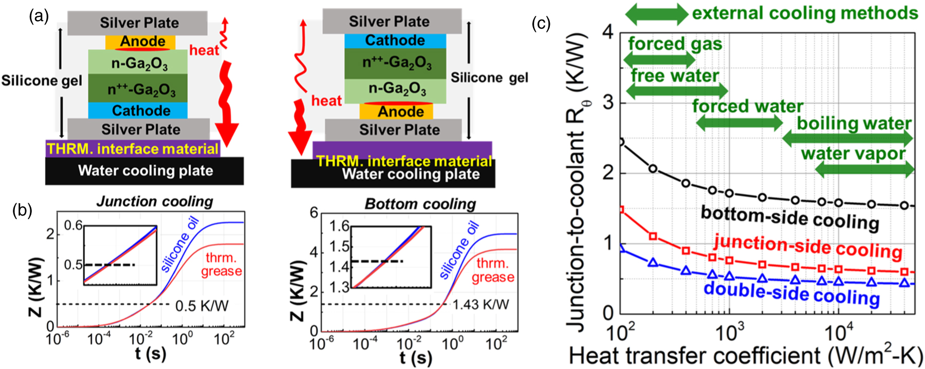
Wang et al. 16) first demonstrated the double-side packaging of 600 V/15 A Ga2O3 SBDs with nanosilver sintering as the die attach and then employed the packaged devices to evaluate the RθJC under the junction- and bottom-side cooling [Fig. 4(a)]. The junction-side cooling allows for heat extraction directly from the device junction instead of through the Ga2O3 chip. From the thermal impedance curves obtained under two thermal interface materials, the RθJC of the packaged device was extracted to be 1.4 K W−1 and 0.5 K W−1 for the bottom-and junction-side-cooling, respectively [Fig. 4(b)]. The RθJC of the junction-side-cooled Ga2O3 SBD is smaller than similarly-rated, TO-packaged commercial SiC SBDs, manifesting the effectiveness of the junction-side cooling to overcome the low kT of Ga2O3.
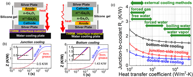
Fig. 4. (Color online) (a) Measurement setup for the junction-to-case thermal resistance of a double-side-packaged Ga2O3 SBD under the bottom-side cooling (left) and junction-side cooling (right). The measurement results are shown in (b). (c) The simulated junction-to-ambient thermal resistance of the bottom-side-, junction-side- and double-side-cooled Ga2O3 SBD with different external cooling approaches [Reprinted from IEEE Electron Device Lett. 42 1132 (2021). 16)]
Download figure:
Standard image High-resolution imageBuilding on RθJC, the authors also simulated the junction to ambient thermal resistance (RθJA) of Ga2O3 SBDs under different external cooling strategies [Fig. 4(c)]. The results confirmed the need for junction-side cooling and suggested deployment of the external cooling with a heat transfer coefficient (HTC) over 103 W m−2·K−1, which can be achieved by the forced water. Double-side cooling can further reduce the RθJA by 30%–40% at the price of the increased complexity, cost, and thermomechanical stress.
For device-level thermal management, despite many simulation studies, 65) experimental works on the large-area, packaged Ga2O3 devices have not been reported until very recently. Willhelmi et al. measured the RθJC of large-area Ga2O3 SBDs with a substrate thickness thinned down to 200 μm. 66) These Ga2O3 SBDs were assembled in standard TO-247 packages by soldering and wire bonding and were cathode-side cooled. The thermal measurements and simulations show that the substrate thinning reduces the device RθJC by more than half as compared to the standard substrate thickness (500 μm). Later simulation results by the same authors 67) revealed the flip-chip assembly for junction-side cooling could further reduce RθJC to be comparable to commercial SiC devices. These results supported the experimental results from Wang and Xiao et al. 16)
By combining the junction-side-cooling package and substrate thinning, Gong et al. 48) demonstrated low RθJC in a 335 V/20 A Ga2O3 SBD [Fig. 5(a)]. Under the junction-side-cooling, the flip-chip Ga2O3 SBD with the thinned substrate (70 μm) showed a RθJC (1.48 K W−1) lower than the device with the 550 μm Ga2O3 substrate (2.71 K W−1) [Fig. 5(b)]. In addition to the steady-state RθJC, the transient RθJC of two devices was measured down to a μs-level time scale. This result suggests that, even with an effective junction-side heat extraction, the substrate thinning may still enhance thermal management by boosting heat extraction through the other side of the chip. The package-level and die-level thermal management need to be co-designed and co-optimized for Ga2O3 power devices. 63)
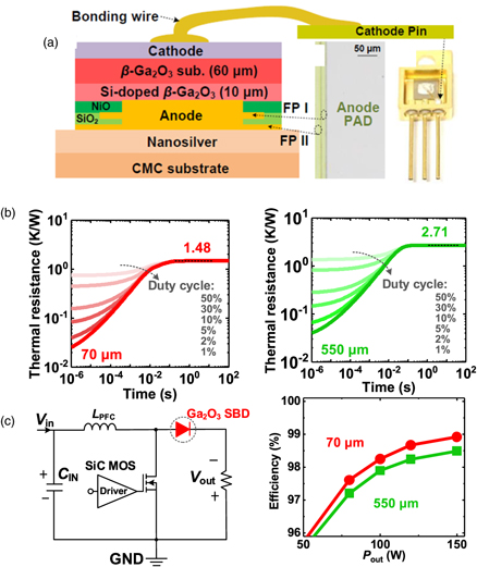
Fig. 5. (Color online) (a) Schematic diagram of the thin-body Ga2O3 SBD with flip-chip packaging. (b) Time-resolved thermal resistance curves of 70 μm thin-body Ga2O3 SBD (left) and 550 μm normal body thickness Ga2O3 SBD (right). (c) Circuit schematic of the boost PFC (left) and system efficiency as a function of the output power (Pout) at a switching frequency of 0.1 MHz [Reprinted from IEEE Electron Device Lett. 43 773 (2022). 48)]
Download figure:
Standard image High-resolution imageA challenge for the package-die thermal co-design is the lack of a modeling framework that interfaces the package- and device-level simulations. 63) Typical package-level finite element analysis (FEA) simulations assume a uniform power dissipation over the device junction neglecting the electrothermal effects (e.g. lattice heating in the sub-micron device structure). Conversely, the typical physics-based device simulations simplify the packaging into a normal boundary thermal resistance or HTC. Recently, Albano et al. 68) investigated a series of models to integrate the physics-based TCAD model with a package-level FEA model for the packaged Ga2O3 power devices, which demonstrated a superior trade-off between the simulation accuracy and computation load. This paves the road for package-die, electrothermal co-design, and co-optimization for Ga2O3 power devices.
4. . Switching performance and circuit applications
Switching performance evaluation and converter demonstrations are key to identifying the market value of the Ga2O3 power device technology. Up to now, the relevant switching studies have been reported in both vertical Ga2O3 diodes and lateral Ga2O3 MOSFETs.
Vertical Ga2O3 diodes have good potential for various applications such as power factor correction (PFC) and active clamp flyback circuits. An essential test for power diodes is the reverse recovery measurements, as the reverse recovery time (trr) is a key limiting factor for the switching speed and loss. It should be mentioned that serious reverse recovery tests should be performed on large-area devices. Otherwise, the waveform could be dominated by the RC discharging time; the large resistance of small-area devices could blind the true reverse recovery process. To date, several research groups have made progress in the switching characterization of large-area vertical Ga2O3 diodes.
Yang et al. 38) reported that the trr of 1 mm2 Ga2O3 SBD was ∼30 ns for switching from +2 V to a relatively small reverse voltage (−5 V). They later reported a 0.785 mm2 Ga2O3 rectifier with Vbr of 760 V. 69) The device showed a trr of 64 ns when switched from 1 A to −300 V with a minimal temperature dependence of trr up to 150 °C. This temperature independence is expected for unipolar conduction.
Gong et al. 19) evaluated the dynamic switching performance of 9 mm2 Ga2O3 HJD and SBD by utilizing the double-pulse-test (DPT) measurements [Fig. 6(a)]. When switched from a forward current of 1.6 A to a reverse bias of 100 V with a fast di/dt of 500 A μs−1, the HJD and SBD exhibit similar switching performance with a trr of 11 ns and a reverse recovery charge (Qrr) of 13 nC, which is comparable to commercial SiC SBD and far outperforms the Si fast-recovery diode (FRD) [Fig. 6(b)]. Even when the device is switched from a high forward current of ∼6.5 A, the HJD still shows almost zero reverse-recovery with a low trr of 12.0 ns [Fig. 6(c)]. This is attributed to the short minority carrier lifetime (4.5 ns) in n-Ga2O3 even at high-level injection. A similar nearly-zero reverse recovery was also reported in GaN native p-n junctions. 35) The small trr suggests that the Ga2O3 HJD could possess the benefits of the bipolar conduction, such as higher current capability and superior robustness, but do not suffer from the trr increase, i.e. the adverse consequence of the bipolar conduction in Si and SiC.
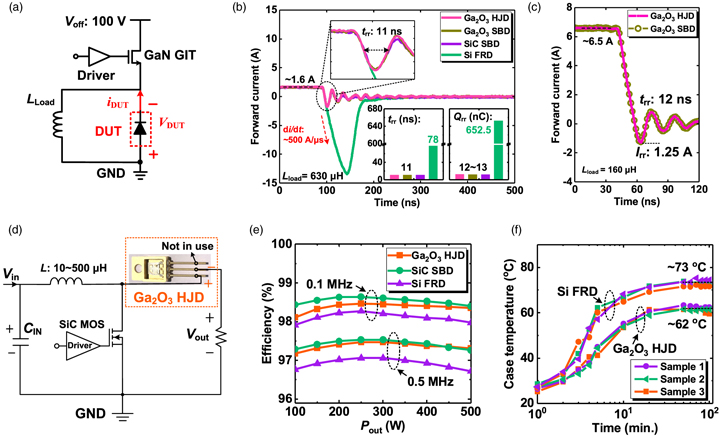
Fig. 6. (Color online) (a) Schematic of the DPT circuit. The fast-speed commercial GaN gate injection transistor (GIT) has been used as a control switch. (b) Reverse recovery characteristics of different diodes. (c) Reverse recovery waveforms with a high forward current of ∼6.5 A. (d) Schematic of the PFC circuit (Vin: 0–310 V, Vout: ∼390 V) with the packaged Ga2O3 HJD. (e) System power-conversion efficiency versus output power (Pout) of a 500 W PFC circuit at switching frequencies of 0.1 and 0.5 MHz. (f) The extracted cast temperature of the 3 samples at 0.3 MHz/500 W [(a)–(c) Reprinted from IEEE Trans. Power Electron. 36 12213 (2021). 19) (d)–(f) Reprinted from IEEE Trans. Power Electron. 37 1223 (2021). 15)]
Download figure:
Standard image High-resolution imageSimilarly, Zhou et al. 15,40) reported a short trr of 16.4 ns and a reverse recovery charge of 34 nC in the 1 mm2 beveled-mesa Ga2O3 HJD assembled in the TO-220 package. Furthermore, the overall correction capability of this device was evaluated in a 500 W PFC converter with long-term continuous operation [Fig. 6(d)]. This device showed good stability in continuous operation and enabled a high power-conversion efficiency of 98.5% and 97.4% at the switching frequency of 0.1 and 0.5 MHz, respectively, which outperformed Si FRDs [Fig. 6(e)]. Figure 6(f) demonstrates that the HJD exhibited a low case temperature of 62 °C at 0.3 MHz/500 W steady-state operation, approximately 11 °C lower than that of commercial Si FRD. Similar converter tests were also performed by Gong et al. 48) on the thin-substrate Ga2O3 SBD as described in Sect. 3 (see Fig. 5). A record high power efficiency of 98.9% at a switching frequency of 0.1 MHz was achieved by the device, which is higher than the device with the standard substrate thickness (and inferior thermal performance) [Fig. 5(c)].
Guo et al. demonstrated a DC-DC converter with the 2 A/467 V Ga2O3 SBDs assembled in a TO-220 package. 70) The trr of 8.8 ns with a Qrr of 8.33 nC was achieved when the device was switched from 1 A to −100 V with a di/dt of 400 A μs−1. The converter showed a high conversion efficiency of up to 95.62% at the input voltage of 200 V and an operating frequency of 100 kHz, which is comparable to that based on a similarly-rated commercial SiC SBD. Later, the same group reported a trr of 26.8 ns in a 5 A/1060 V Ga2O3 JBS diode. 71) They further used this device to demonstrate a four-stage hybrid half-wave Cockcroft-Walton voltage multiplier. The hybrid circuit using the Ga2O3 JBS and SiC SBD showed a multiplication factor of 3.81, being comparable to the factor of all SiC SBD circuits. A high circuit efficiency of 86.07% was also demonstrated. The above results show the gigantic potential of vertical Ga2O3 power diodes for low switching loss, high conversion efficiency, and high-temperature power electronics applications.
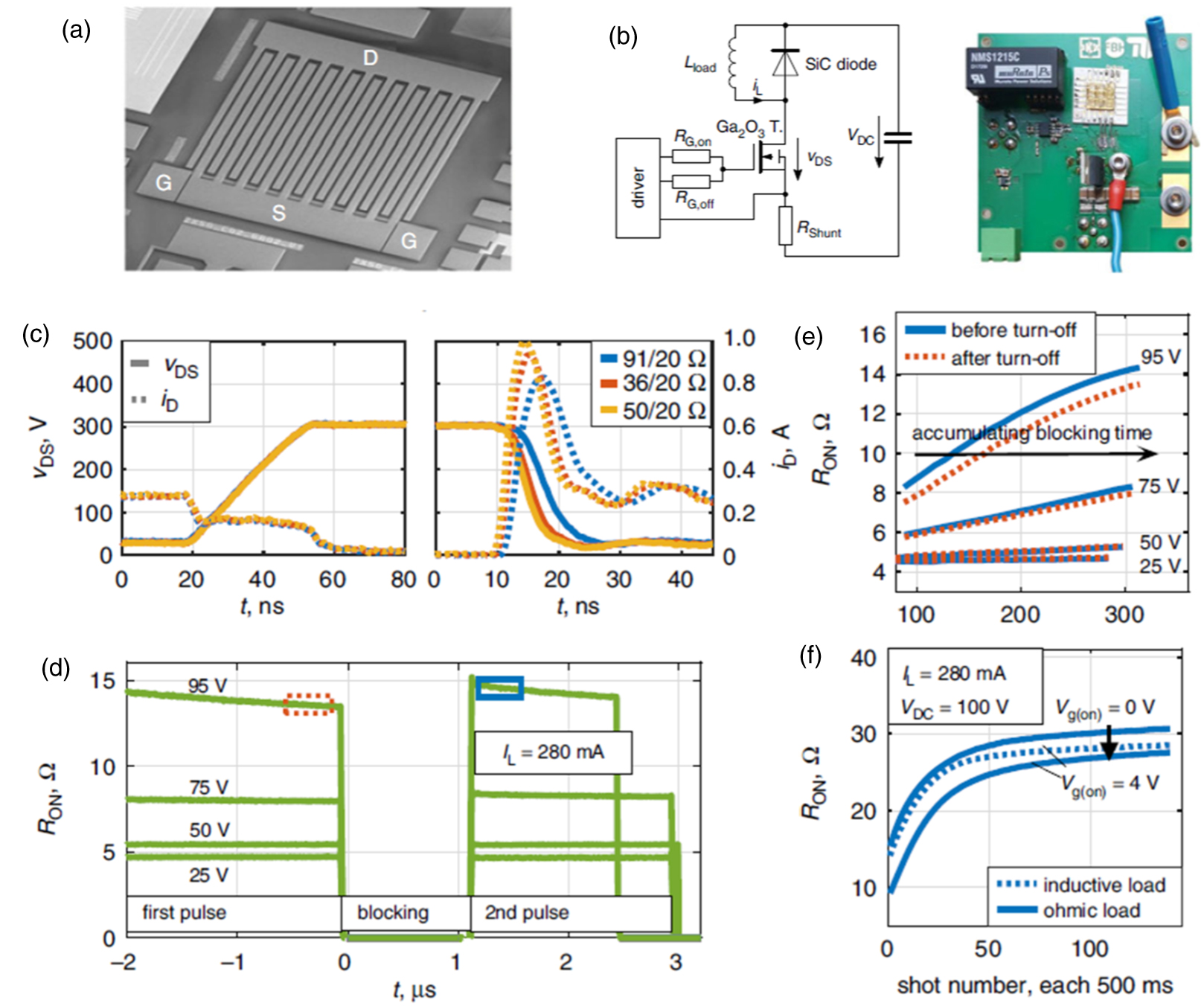
Static characteristics and switching performance of lateral Ga2O3 MOSFET have also been investigated. 17,18) J. Böcker et al. reported a large-area lateral Ga2O3 MOSFET with a Ron of 5 Ω and forward saturation current up to 2.5 A, as shown in Fig. 7(a). 18) DPT setup shown in Fig. 7(b) is employed to evaluate the high-voltage switching dynamics. Figure 7(c) shows the hard-switching performance under different gate resistances. The voltage slope during turn-on increased from 35 to 50 V ns−1 by reducing the gate resistance from 91 to 36 Ω at an input voltage of 300 V. The dynamics Ron under different DC voltages, load currents and load conditions, as well as the increased blocking time, were investigated to determine the impact and origin of the charge trapping effect [Figs. 7(d)–7(f)]. The Ron was found to increase obviously by applying a DC voltage for 1 s before the DPT. Only a small further increase was observed after 1 μs blocking and the following turn-on process [Fig. 7(d)]. The increased blocking time also resulted in Ron increase during the repetitive DPT [Fig. 7(e)]. Figure 7(f) showed that the Ron dynamic increase could be mitigated by increasing the turn-on driver voltage. These results suggested that the charge trapping during the blocking process in the gate region mainly resulted in the dynamics Ron increase.

Fig. 7. (Color online) (a) A photograph of the lateral Ga2O3 MOSFET. (b) Circuit test setup for the DPT. (c) Switching characteristics of the lateral Ga2O3 MOSFET with different gate resistance. Ron dynamics during DPT (d) at different DC voltages, (e) before and after the blocking period for rising load currents, and (f) with ohmic and inductive load, as well as different turn-on driver voltages. [Reprinted from Electron. Lett. 56 838 (2020). 18)]
Download figure:
Standard image High-resolution imageAfterward, the same group reported the hard-switching characteristics of large-area lateral MOSFET with a bus voltage increased up to 400 V. 17) A higher turn-on speed of 78 V ns−1 was demonstrated by utilizing the FP structure and improving the fabrication process. Similar dynamics Ron issues were found during the hard-switching operation. Hence, device innovation and process improvement should be focused on future research to mitigate the current dispersion and dynamics Ron increase under the dynamic switching.
5. . Ruggedness
Power devices are required to possess ruggedness against abnormal operations outside the safe operating area for a sufficient time before the protection circuitry intervenes. Such abnormal operations involve overvoltage and overcurrent far exceeding the rated values. The corresponding ruggedness for power diodes mainly includes (1) the avalanche or overvoltage ruggedness, 5,72,73) which measures the device capability to withstand transient surge energy or overvoltage in the off-state, and (2) the surge current ruggedness, 35) which measures the device capability to withstand transient overcurrent in the on-state. For power transistors, in addition to the avalanche/overvoltage ruggedness, the short-circuit ruggedness measures the device capability to withstand the transient overcurrent not only in the on-state but also in the high-bias blocking state. 34) Meanwhile, gate ruggedness is also important for power transistors. 74)
The ruggedness is a critical concern for Ga2O3 power devices due to the high junction E-field and low kT of Ga2O3. As most ruggedness involves the electrothermal, transient, non-equilibrium process, it has to be characterized on large-area, packaged devices in circuit tests. The measurement results for on-wafer, small-area devices are usually less meaningful, as there are no straightforward scaling laws to use these results to project the ruggedness of practical devices. Very recently, thanks to the progress on Ga2O3 large-area devices, a few groups have experimentally investigated the surge current and overvoltage ruggedness of Ga2O3 diodes. Meanwhile, simulation investigations have been reported on the short-circuit ruggedness of Ga2O3 transistors.
Surge current is an essential ruggedness metric listed in any power diode's datasheet. A surge-current test circuit usually produces a 10 ms wide half-sinusoidal current waveform based on the JEDEC standard. Buttay et al. 75) first studied the surge current capability of Ga2O3 diodes using the device model and the SPICE network model; junction-side cooling was identified to be an effective pathway to boost the surge ruggedness. Following this theoretical study, Xiao and Wang et al. 20) reported the first experimental studies of the surge current ruggedness of Ga2O3 SBDs assembled in the bottom-side and double-side cooling package. As shown in Figs. 8(a)–8(c), a 1 mm thick Ag plate was deployed to confine the heat diffusion during the 10 ms transient and thus eliminate the impact of the outer solder, DBC, and wire bonds. The surge-current tests revealed a critical surge current of 37.5 A for the bottom-side-packaged Ga2O3 SBD and 68 A for the double-side-packaged Ga2O3 SBD [Fig. 8(d)].
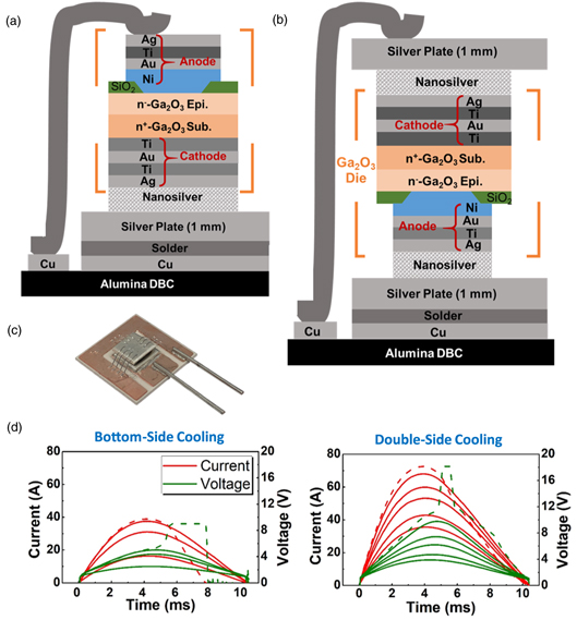
Fig. 8. (Color online) (a) Schematics of Ga2O3 SBDs assembled in the (a) bottom-side cooling package and (b) double-side cooling package. (c) Photo of the prototyped double-side packaged Ga2O3 SBDs. (d) Surge current test waveforms of the two packaged Ga2O3 SBDs with the increased surge current magnitude. [Reprinted from IEEE Trans. Power Electron. 36 8565 (2021). 20)]
Download figure:
Standard image High-resolution imageThe higher surge current capability of the double-side-packaged Ga2O3 SBD is attributable to the effective heat removal through the junction and the resultant migration of the peak temperature location. This was illustrated by the results of the electrothermal, device-circuit, mixed-mode TCAD simulations. 20) At the high surge current transient, in a double-side-packaged Ga2O3 SBDs, the simulated heat flux contour reveals that most heat is removed through the junction [Fig. 9(a)], and the peak temperature location moves from the Schottky junction into the bulk Ga2O3 [Fig. 9(b)]. As the bulk semiconductor is usually more thermally robust as compared to the heterogenous interface, a higher peak temperature (and higher surge current capability) can be accommodated.

Fig. 9. (Color online) The simulated contours of (a) heat flux and (b) temperature in the Ga2O3 SBD junction region at the surge current transient. (c) Projected peak temperature as a function of peak surge current for the Ga2O3 SBDs with different thermal management techniques (bottom/double-side package, 0.1/0.5 mm substrate thickness, transfer to SiC substrate) and a reference SiC SBD. [Reprinted from IEEE Trans. Power Electron. 36 8565 (2021). 20)]
Download figure:
Standard image High-resolution image
The other interesting finding in Ref. 20 is that the packaged Ga2O3 SBDs show a superior surge current capability as compared to the similarly-rated commercial SiC SBDs. In addition to the effective junction-side heat removal, a key enabling mechanism is the smaller temperature coefficient of the differential on-resistance (α) in Ga2O3 SBDs (α ∼ 0.73) as compared to that in SiC SBDs (α > 2.5), which suppress the positive feedback of the increase in on-resistance and junction temperature. The critical role of α on the surge current capability was also confirmed in GaN, where the negative α of GaN p-n diodes enables a high surge current. 35) The physical mechanism of the low α of Ga2O3 SBDs could be related to the deep donors but requires further investigation. 20) The authors in Ref. 20 also used the calibrated simulation models to explore the approaches to further improve the surge current capability of Ga2O3 SBDs [Fig. 9(c)]. The Ga2O3 integration with the high-kT substrate, in the combination with the double-side-cooling package, is predicted to be the most effective way.
Gong et al. 19) recently reported the surge current ruggedness of Ga2O3 HJDs and SBDs assembled in the TO-220 package. The Ga2O3/NiO HJDs exhibit a higher surge current capability than SBD, possibly due to the negative α observed in HJDs. These results suggest the Ga2O3/NiO p-n junction possesses the functionality to boost the surge current ruggedness similar to the homogenous p-n junction in GaN and SiC. Later, the authors 48) reported the surge current capability of the junction-side-packaged Ga2O3 SBDs with the thinned substrate [see Fig. 5(a)]. A critical surge current (59 A) much higher than the TO-packaged Ga2O3 SBD (38 A) 19) was demonstrated, further manifesting the importance of packaging on the surge current ruggedness of Ga2O3 devices.
Avalanche is a desirable capability for power devices to withstand overvoltage stresses, as it relies on impact ionization and multiplication to allow devices to pass a high current at the non-destructive Vbr. 5) However, not all power devices come with the avalanche capability: it is absent in commercial GaN high-electron mobility transistors 5) but equipped in most Si and SiC devices as well as some other GaN bipolar devices. 21,29–32) As the avalanche in Si, SiC and GaN devices all rely on native p-n junctions, it could be very difficult to realize the avalanche-capable Ga2O3 devices due to the lack of the p-type Ga2O3. Hence, for the overvoltage ruggedness of Ga2O3 devices, a very good reference is the GaN HEMT. Recent studies of the GaN HEMT overvoltage ruggedness converge on several key conclusions: (1) the device relies on the overvoltage margin and output capacitance to withstand the overvoltage stress without the capability to dissipate the surge energy, 5,73,76) (2) the overvoltage ruggedness can be characterized by the unclamped inductive switching (UIS) circuit, 5) and (3) the Vbr in short switching transient (i.e. dynamic Vbr) could be very different from (usually larger) that measured on the curve tracer (i.e. static Vbr). 76–78)
Recently, Zhou et al. 15) reported the overvoltage ruggedness of large-area Ga2O3/NiO HJDs using single-pulse and repetitive UIS circuits. The Ga2O3 HJD exhibits a static Vbr of 1.95 kV and a dynamic Vbr of 2.23 kV, suggesting an increased overvoltage margin in dynamic switching. In addition, the Ga2O3 HJD shows no parametric shifts after 1 million cycles if UIS stresses with a peak overvoltage of 1.2 kV. This result demonstrates the good overvoltage ruggedness with a withstanding physics similar to GaN HEMTs in Ga2O3 power devices.
Very recently, Lu et al. 79) reported a numerical simulation on the short-circuit ruggedness of a kV-class vertical Ga2O3 power FinFET at the blocking voltage of 800 V. The FinFET is an emerging power transistor first developed in GaN 1,23,24) and later demonstrated in Ga2O3 80,81) with state-of-the-art performance in Ga2O3 power transistors. The forward conduction and breakdown mechanism both hinge on the fin channel design, 82–84) and switching performance also depends on the inter-fin designs. 85) The short-circuit analysis of vertical Ga2O3 FinFETs suggests the strong impact of the inter-fin architectures on the device short-circuit withstanding time (SCWT). 79) The full-gate structure has the worst SCWT due to electrostatics; the split-gate structure can increase the SCWT at the price of Vbr degradation. The simulation predicts that the split-gate design with the inter-fin source coverage could provide the best trade-off between the short-circuit ruggedness and Vbr in vertical Ga2O3 power FinFETs.
6. . Summary and research needs
This paper provides a timely review of the state-of-the-art of the large-area Ga2O3 power devices. The key takeaways include:
- 1)Ampere-class Ga2O3 power diodes (SBDs, JBS diodes, and HJDs) and MOSFETs have been widely reported with Vbr up to >2 kV and 400 V for diodes and MOSFETs, respectively. The performance of most devices is superior to the Si counterparts but still inferior to the SiC and GaN ones. The junction field of several large-area Ga2O3 HJDs has surpassed the EC of SiC or GaN, fulfilling the superior electrical properties of Ga2O3.
- 2)Junction-side packaging and cooling are essential for the thermal management of Ga2O3 power devices, and they can overcome the low-kT limitations of the Ga2O3 material to deliver a low device RθJC. Die-level thermal management such as heterogenous integration and substrate thinning are desirable to be further combined with the junction-side or double-side packaging.
- 3)Ga2O3 SBDs and HJDs have shown minimal reverse recovery and have been applied in a variety of power converters to achieve high power-conversion efficiency. Ga2O3 MOSFETs have exhibited fast switching speed in inductive power switching.
- 4)The surge current capability and overvoltage ruggedness of Ga2O3 SBDs and HJDs have been demonstrated to be comparable or even superior to some SiC and GaN counterparts. Device architectures (e.g. channel design), packaging and cooling, and material properties (e.g. deep dopants) all impact the ruggedness of Ga2O3 devices in an interdependent way.
- 5)The NiO/Ga2O3 heterogenous p-n junction exhibits promising characteristics for power devices, including good current and voltage scalability, minimal reverse recovery, and excellent surge-current and overvoltage ruggedness. It could become an important building block for many advanced Ga2O3 diodes and transistors.
Despite the exciting progress, the research of large-area Ga2O3 power devices is still in the early stage. We envision the following immediate research gaps that need to be addressed for advancing Ga2O3 into industrial power electronics applications.
- 1)P-n junctions form the blocking block for nearly all power devices with avalanche capability and overcurrent robustness. Despite the numerous advantages offered by the UWBG material, the absence of p-type Ga2O3 conductivity may make it difficult to fully utilize these advantages. Although Ga2O3 p-n heterojunction has emerged as an alternative bipolar design to deliver superior performance than the SBD counterparts, the fundamental challenge is the mismatch of bandgap and critical electrical field strength that may hinder the electric-field handling capability. Another important consideration is the interface engineering in such heterojunctions, where interfacial traps and impurities would degrade the electrical performance and reliability robustness.
- 2)Defect reduction is key to boosting the performance of large-area devices. Deep-level defects/traps within Ga2O3 bulk and interfacial regions generally act as carrier generation-recombination (G-R) centers, which are the dominant sources to degrade device performance and reliability. Defects may be unintentionally-introduced impurities or intrinsic crystalline defects (dislocations or stacking faults) that are energetically formed and inhomogeneously distributed during material growth. Therefore, the fundamental challenge in the material aspect, reducing defects and dislocations, is crucial to enhance carrier transport and improve device performance.
- 3)Junction capacitance and switching charges are critical for power devices; to enable advantages in practical power devices, the low Ron,sp has to be converted to the realization of smaller capacitances and charges. 1) However, the relevant studies are quite scarce in Ga2O3. Very recent work reported the capacitance, charges, and switching figure-of-merits (FOMs) of Ga2O3 SBDs for the first time, 86) while the switching FOM is still inferior to the commercial SiC SBDs. A rigorous study of the impact of the low carrier mobility in Ga2O3 on the switching FOMs of Ga2O3 devices for different applications (e.g. soft-switching, hard-switching) is highly desirable to understand Ga2O3's true application space in power electronics.
- 4)Device innovations are highly desirable to further improve the junction E-field in large-area Ga2O3 devices and ensure it would not compromise in devices with the upscaled current and voltage ratings. While the average junction E-field calculated in many papers of small-area Ga2O3 devices could be a good indicator of the material limit, it does not mean any true advantage in power device performance, particularly for devices with low Vbr. Currently, the junction E-field in ampere-class, high-voltage Ga2O3 devices is still much lower than that reported in small-area Ga2O3 devices with low Vbr.
- 5)The fundamentals of the Ga2O3 heterogeneous p-n junction in power switching, particularly the carrier dynamics under the non-equilibrium, transient switching conditions, are important for understanding the device switching and ruggedness characteristics. In addition, the feasibility of avalanche in heterogeneous p-n junction remains an open question. The avalanche capability, if achievable in heterogeneous junctions, could be a strong boost to not only the ruggedness but also the performance of Ga2O3 power devices (as the Vbr margin required for a specific voltage rating could be much smaller for avalanche-capable power devices).
We envision that Ga2O3 power devices hold tremendous potential for penetration into power electronics applications if these gaps can be addressed in the next few years.
Acknowledgments
We appreciate the in-person discussions with Ga2O3 researchers in IWGO2022. The work at Virginia Tech is in part supported by National Science Foundation under Grants ECCS-2100504 and ECCS-2230412 and in part by the Center for Power Electronics Systems High Density Integration Industry Consortium.