

Abstract
In the past few years, graphene has drawn interest for applications in optoelectronic devices. Due to its extraordinary properties, i.e. wide optical bandwidth, tunable absorption, high carrier mobility, and CMOS compatibility, it is a candidate to improve current state-of-the-art high-speed optoelectronic devices, such as modulators. In this work, we present a model that describes the DC and high-speed behaviour of single-layer graphene-oxide-silicon electro-absorption modulators (EAM). We compare the theoretical analysis with experimental results, and we find that p-doped graphene combined with p-doped silicon enables high-speed operation at low DC bias. Using this configuration, we demonstrate 75 μm long TM EAMs operating in the O-band and in the C-band. The O-band EAM exhibits 3.1 dB extinction ratio (ER) and 16.0 GHz 3 dB bandwidth at 1 V DC bias. With the C-band EAM we achieve 6.5 dB ER and 14.2 GHz 3 dB bandwidth at 0 V DC bias. Open eye diagrams up to 50 Gbit s−1 are measured using 2.5 Vpp and −0.5 V DC bias at a wavelength of 1560 nm.
Export citation and abstract BibTeX RIS
1. Introduction
Electro-optical modulators are key components in optical communication systems. Important requirements for modulators are low insertion loss (IL), high extinction ratio (ER), high operation speed and low energy consumption.
In the past few years, graphene, a two-dimensional network of sp2-hybridised carbon atoms, has attracted a lot of interest due to its unique optoelectronic properties.1–3) Graphene is a zero bandgap material, with an optical bandwidth from visible to infrared (up to 180 nm in the C-band).4,5) It absorbs 2.3% of the perpendicularly incident light, which can be enhanced further by integrating graphene on a waveguide to increase the interaction length between light and graphene. Graphene's absorption can be easily tuned through capacitive charging by applying an electric field,2) and has therefore the potential to enable active optoelectronic functionality onto passive optical waveguides, such as Si and low-loss SiN waveguides.6) In addition, graphene is CMOS compatible and can be integrated into CMOS processes in the back end of line. These properties, together with the high carrier mobility (e.g. more than 300 000 cm2 V−1 s−1 with hBN encapsulation7)), make graphene a candidate for applications in high-speed optoelectronic devices, such as photodetectors8–13) and modulators.4,5,13–21)
High-speed graphene modulators have been reported in literature in single-layer graphene (SLG)4,5,15,19) or double-layer graphene (DLG)13,14,20,21) configuration on top of the waveguide. DLG modulators are based on a graphene-oxide-graphene capacitor, while SLG modulators are based on a graphene-oxide-silicon (GOS) capacitor. Due to the presence of two graphene layers, DLG modulators offer potential for higher ER than SLG modulators, but they suffer from higher IL. In addition, SLG modulators have a simpler fabrication process compared to DLG modulators, requiring the transfer of only one graphene layer. A DLG ring modulator with 30 GHz 3 dB frequency response and open eye diagrams at 22 Gbit s−1 was demonstrated by reducing the capacitance of the device using a 65 nm thick Al2O3 as spacer between the two graphene layers.14) However, employing a thick Al2O3 comes at the expense of the high drive voltage (7.5 Vpp) and high DC bias (−30 V) necessary to operate the device. In addition, the device has limited optical bandwidth, due to the resonant nature of the ring modulator. A more recent work reports a 120 μm long DLG electro-absorption modulator (EAM), built on top of a silicon waveguide with a 20 nm thick SiN spacer between the two graphene layers, exhibiting 20 dB IL and 3 dB ER for 9 Vpp.21) The device shows 29 GHz 3 dB frequency response and open eye diagrams at 50 Gbit s−1 using 3.5 Vpp, at a high DC bias of 8 V. Among SLG modulators, in5) a broadband SLG EAM with a n-doped Si waveguide was demonstrated, achieving a 3 dB frequency response of 5.9 GHz and open eye diagrams at 10 Gbit s−1 using 2.5 Vpp at 1.75 V DC bias in the wavelength range between 1530 and 1565 nm. In,15) a 50 μm long SLG EAM with a p-doped Si waveguide was demonstrated, exhibiting an improved 3 dB frequency response of 16 GHz at 0 V DC bias and open eye diagrams up to 25 Gbit s−1 using 2.5 Vpp at 2 V DC bias.
In this paper, we present a theoretical model that describes the DC and high-speed performance of SLG EAMs. The model is used to identify the optimal combination of graphene doping and silicon waveguide doping, in order to optimise the DC performance and the total device RC for high-speed operation around 0 V DC bias. We compare experimental results from three samples, fabricated by transferring graphene on waveguides with different type and level of silicon doping, to corroborate the theoretical analysis. After transfer, graphene on waveguides exhibits p-doping behaviour. We employ a thin SiO2 layer with a thickness of 5 nm as spacer between graphene and Si, in order to achieve a low operating bias. The best static and high-speed performance is obtained on TM SLG EAMs fabricated with p-doped silicon waveguides. O-band and C-band operation with more than 14 GHz 3 dB frequency response is demonstrated across a total wavelength range of 140 nm. On a 75 μm long O-band TM SLG EAM, we achieve 4.0 dB IL, 3.1 dB ER using 8 Vpp and 16.0 GHz 3 dB frequency response at 1 V DC bias at 1300 nm wavelength. In the C-band, we demonstrate a 75 μm long broadband SLG EAM with 4.2 dB IL, 6.5 dB ER using 8 Vpp and 14.2 GHz 3 dB frequency response at 0 V DC bias and 1560 nm wavelength. Open eye diagrams are obtained up to 50 Gbit s−1 at 1560 nm wavelength for the first time on a SLG EAM, using 2.5 Vpp and −0.5 V DC bias, thus showing potential for graphene integration in high-speed photonics applications.
2. Device design and fabrication
The SLG-silicon EAM is based on a 220 nm thick silicon (Si) waveguide, fabricated on a silicon-on-insulator (SOI) wafer with 2 μm buried oxide in imec's 200 mm Si photonics platform [Fig. 1(a)].22) The waveguide is partially etched on one side, creating a rib structure that allows to contact the Si waveguide through the 70 nm thick slab layer. The waveguide is embedded in SiO2 to ensure a planar surface for the subsequent graphene transfer. Three separate doping levels ( for the contact region,
  for the slab region,
  for the waveguide region) are used to minimise the Si contact and sheet resistance, without significantly increasing the waveguide loss. After Si waveguide patterning, a chemical-mechanical planarisation step is performed to planarise the waveguides. Through thermal oxide growth the desired SiO2 thickness of 5 nm is obtained on top of the Si waveguide. After wafer dicing, subsequent processing is performed at coupon level in a cleanroom lab environment. Graphene grown by chemical vapour deposition is transferred on top of the Si waveguides. Both growth and transfer processes were carried out by Graphenea (www.graphenea.com. Subsequently,graphene is patterned to cover part of the Si waveguide and to define the length of the EAM. Contacts are made to graphene (50 nm Pd) and to the doped Si (10 nm Ti/20 nm Pt/50 nm Au) based on a standard lift-off process. These contact metals were selected to minimise the contact resistance to graphene and to Si respectively.23) The contacts are placed 2 μm away from the waveguide and therefore have no impact on transmission loss. The graphene and silicon contacts are used to apply an electric field across the device, which modulates the Fermi level in graphene.

Fig. 1. (Color online) (a) Schematic cross section of the SLG EAM. The three doped silicon regions are either p- or n-doped: waveguide ( ), slab (
 ) and contact (
 ). The graphene, oxide and silicon layers form a GOS capacitor. (b) Equivalent electrical circuit of the SLG EAM. The RC constant limits the 3 dB frequency response.
Download figure:
Standard image High-resolution image3. Device modeling
3.1. Static electro-optical behaviour of the SLG EAM
The static electro-optical behaviour of the SLG EAM is defined by the relation between the absorption and graphene's Fermi level μ. Graphene's absorption is derived from the 2D complex optical conductivity  , calculated from the Kubo formula.2) This formula takes into account interband and intraband transitions, and it depends on the angular frequency ω, the charged particle scattering rate ℏΓ, the temperature T, and most importantly graphene's Fermi level μ. The latter can be shifted by sweeping the voltage Vg across the GOS capacitor,2) according to
where q is the elementary charge, ℏ is the reduced Planck constant, vF is the Fermi velocity of carriers in graphene and CGOS is the capacitance of the GOS capacitor. The Fermi level μ is the sum of two contributions:

μ0 is the initial Fermi level position due to the fixed number of charges n0 (graphene's intrinsic doping), and Δμ is the Fermi level shift caused by the number of charges ns accumulated on graphene when we apply Vg across the capacitor.
The static electro-optical behaviour of the SLG EAM as a function of applied voltage is mainly affected by two parameters: graphene's intrinsic doping (n0) and the scattering rate ℏΓ. The intrinsic doping n0 affects the position of minimum transmission as a function of applied voltage. Figure 2(a) shows the simulation, performed using Lumerical MODE Solutions, of the optical transmission as a function of gate voltage for a TE SLG EAM with 5 nm thick SiO2 and 500 nm wide waveguide operating at 1560 nm, for neutral (n0 = 0 cm−2) and p-doped ( ) graphene, for scattering rate ℏΓ = 15 meV. For neutral graphene, the minimum is at 0 V, therefore switching between high transmission (on-state) and low transmission (off-state) requires ∼3.5 or ∼−4 V DC bias. For p-doped graphene, the minimum transmission point is shifted to negative bias. In this case, switching occurs between −2 and 2 V, which is compatible with current CMOS technology. The scattering rate ℏΓ, which is inversely proportional to the mobility μ,24) affects the ER of the modulator. As shown in Fig. 2(b), a lower scattering rate, implying higher graphene quality, results in higher ER for a given Vpp because graphene can reach full transparency. For example, a 75 μm long SLG EAM would show 0.5 dB higher ER for ℏΓ = 0.43 eV compared to ℏΓ=30 eV. In real applications, graphene's scattering rate is often more than 10 meV,24) resulting in a reduced ER and increased IL.

Fig. 2. (Color online) Simulated transmission as a function of gate voltage at λ = 1560 nm of a TE SLG EAM with 5 nm oxide, 500 nm wide waveguide and  cm−3: (a) for neutral (n0 = 0 cm−2) and p-doped (
 ) graphene, with graphene's scattering rate ℏΓ = 15 meV; (b) for p-doped graphene (
 ) and scattering rates ℏΓ = 0.43, 15, 30 meV. When graphene is p-doped the switch between on- and off-state occurs between −2 and 2 V. Higher scattering rate results in lower ER and higher IL.
Download figure:
Standard image High-resolution image3.2. RC limited high-speed behaviour of the SLG EAM
The 3 dB frequency response of a SLG EAM is limited by the RC constant of the device, and can be explained using the equivalent electrical circuit in Fig. 1(b).
3.2.1. Device resistance
The device total resistance (Rtot) is the sum of graphene's contact and sheet resistance (RgraC and Rgra) and the Si contact and sheet resistance (RSiC and RSi). Graphene's resistance is affected by the scattering rate ℏΓ, which is proportional to the impurity density  , caused by local potential fluctuations and electron/hole puddles on the graphene layer.25,26) Higher scattering rate corresponds to lower mobility and therefore higher resistance. When the mobility is higher (lower ℏΓ and
  ), the peak in graphene's resistance corresponding to the neutrality point is higher. As a consequence, the resistance experiences a more abrupt change when the gate voltage is increased or decreased to move away from the neutrality point.24) The values of RgraC and Rgra at a fixed DC voltage bias are also affected by graphene's intrinsic doping n0. For n0 = 0, graphene's resistance reaches its peak value at 0 V voltage bias, and decreases for increasing (or decreasing) voltage bias. When applying Vgate as indicated in Fig. 1(a), p-doped (n-doped) graphene shows a peak value at negative (positive) voltage bias due to the shift of graphene's charge neutrality point [Fig. 3(a)]. The resistance then decreases as the voltage increases (decreases). In case of p-doped graphene, there is therefore a low resistance region for voltage values around or greater than 0 V. The Si contribution to Rtot depends on the doping level of the three Si regions: contact, slab and waveguide areas. To properly estimate how the silicon doping impacts the resistance, we perform a process simulation using Sentaurus TCAD, which accurately emulates the real processing performed in the fab. Afterwards we extract the values of silicon resistance (RSi and RSiC) for the three doped regions together (contact, slab and waveguide) by performing a transient device simulation at different voltage values. Figure 3(b) shows the values of Rtot as a function of gate voltage for a 75 μm long device with p-doped graphene (mobility μc = 800 cm2 V−1 s−1; RgraC = 880 Ω μm and Rgra = 340Ω/□at 0 V) and a waveguide width of 500 nm, for p-doped (pwg = 1.9 × 1018 cm−3, pslab = 3.2 × 1019 cm−3) and n-doped (nwg = 2.3 × 1018 cm−3, nslab = 2.7 × 1019 cm−3) Si. p-doped silicon exhibits higher sheet resistance than n-doped silicon, due to the lower mobility of holes compared to electrons. The variation of Rtot with gate voltage is influenced by the voltage-dependent behaviour of RgraC(V) and Rgra(V) only.

Fig. 3. (Color online) (a) Graphene resistance as a function of gate voltage for n-doped, neutral and p-doped graphene. For p-doped graphene there is a low resistance region for voltage values around or greater than 0 V. The plotted graph is a visualisation modified from an experimental curve. (b) Simulated total resistance as a function of gate voltage of a 75 μm long SLG EAM with p-doped graphene ( ), for p-doped (pwg = 1.9 × 1018 cm−3, pslab = 3.2 × 1019 cm−3) and n-doped silicon (
 ). P-doped silicon exhibits higher sheet resistance than n-doped silicon. The voltage-dependent behaviour is caused by RgraC and Rgra.
Download figure:
Standard image High-resolution image3.2.2. GOS capacitance
The total GOS capacitance CGOS is given by the series of graphene's quantum capacitance Cq, the oxide capacitance Cox and the Si depletion capacitance CSi:

Graphene's quantum capacitance is given by the following equation27,28):

where μ is graphene's Fermi level as defined in Eq. (2). The quantum capacitance is characterised by a minimum when μ = 0 [Δμ = −μ0, according to Eq. (2)] and it increases linearly for  [Fig. 4(a)]. For intrinsic (undoped) graphene, the Fermi level is at the Dirac point, μ0 = 0 and therefore Cq = 0 for Δμ = 0 [Fig. 4(b)]. In p-doped (n-doped) graphene, μ0 < 0 (μ0 > 0) and, as a consequence, the minimum of Cq is located at Δμ = −μ0 [Fig. 4(b)]. When graphene is not pristine, the additional impurity carrier density
  should be included in the calculation, The quantum capacitance becomes26)

If we compare Cq with Cox calculated for 5 nm of SiO2 (Fig. 4), we see that the latter is significantly smaller for each value of μ away from the neutrality point. When  , the minimum of the quantum capacitance increases and Cq becomes significantly higher than Cox for any value of chemical potential, as shown by the dotted lines in Fig. 4. For this reason, when placed in series with Cox, the contribution of Cq is minor.

Fig. 4. (Color online) (a) Calculated graphene quantum capacitance as a function of graphene's Fermi level μ, for n-doped ( ), neutral (n0 = 0 cm−2) and p-doped (
 ) graphene, compared with the capacitance of 5 nm thick SiO2. The full lines are calculated for
  and the dotted lines for
  cm−2. (b) Same as (a), but the capacitance is plotted as a function of Fermi level shift (
 ).
).
Download figure:
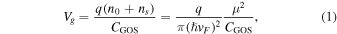
Standard image High-resolution imageThe analytical model used to calculate CGOS as a function of applied voltage Vg is based on the MOS capacitor model,29) with the difference that for the GOS capacitor graphene's quantum capacitance Cq is included in the calculation. The voltage is applied on the graphene contact, while the silicon contact is grounded. In accumulation, when Vg < VFB < 0 for p-doped Si and Vg > VFB > 0 for n-doped Si, with VFB being the commonly known flatband voltage of a MOS capacitor,29) the silicon layer is not yet depleted, so the quantities that play a role are Cq and Cox. To calculate the amount of charges ns accumulated on the graphene layer for each Vg < VFB, we need to solve the following system
where Qacc is the accumulation charge. The resulting equation for ns is
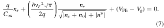
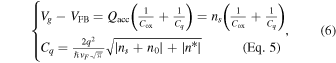
Once the value of ns for each Vg is known, we can calculate Cq through Eq. (4) and therefore the total accumulation capacitance  . Graphene's natural doping n0 is considered in the calculation as an initial condition and it will automatically affect the position of graphene's charge neutrality point in the final result. In fact, ns and n0 in Eq. (4) are summed up before applying the absolute value, which is necessary to make a distinction between n-doped (n0 < 0) and p-doped graphene (n0 > 0). In inversion (Vg > VT > 0 for p-doped Si and Vg < VT < 0 for n-doped Si, where VT is threshold voltage29)) the silicon layer has reached maximum depletion and the quantities to be considered are Cq, Cox and
  . Equation (7) becomes
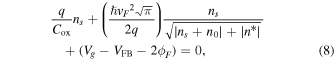
where the bulk potential  takes into account the voltage drop due to
  . The total inversion capacitance can be calculated as
  , where
  is the maximum width of the depletion region in the silicon layer.
To calculate the total capacitance  in depletion (
 for p-doped Si and
  for n-doped Si), a different approach is necessary. The width of the depletion region in silicon Wdep has to be calculated for values of the surface potential
  ranging from 0 to
  . From Wdep, the depletion charge Qdep and therefore the number of charges on graphene ns can be calculated. The total GOS capacitance in depletion is given by
  . All the quantities that have been calculated as a function of
  can then be expressed as a function of the applied voltage through
  .
.
Throughout the calculation of CGOS, the values of  , and therefore
  , are extracted step by step, and are used to obtain graphene's absorption (and therefore transmission) as a function of the applied voltage Vg through Eq. (1), as shown in Fig. 2.
The results of the calculation of CGOS for a GOS capacitor with p-doped silicon ( ) for n-doped (
 ), neutral (n0 = 0 cm−2) and p-doped (
 ) graphene is shown in Fig. 5(b). As expected, graphene's quantum capacitance affects CGOS only where Cq reaches its minimum [Fig. 5(a)]. This effect is clearly visible only when the GOS capacitor is in accumulation mode, and therefore CGOS is higher. As a consequence, reducing Cq by reducing the impurity density
  would only have a small effect on CGOS as a whole. In order to decrease Cox, we could use an oxide with a lower permittivity or increase the oxide thickness. However, both solutions would increase the field necessary to accumulate charges on the capacitor plates in the whole range necessary to operate the device. In other words, the lower capacitance would allow to obtain a higher 3 dB frequency response, but the ER for the same voltage range would be significantly reduced. The device capacitance can therefore be optimised by focusing on how CSi changes when varying the type and level of doping, and on how this affects CGOS. Figure 6 shows the calculation of CGOS performed for p-doped graphene (
 ) for different levels of p-type and n-type silicon doping. The capacitance in accumulation is not affected by the variation in silicon doping level. A reduction in capacitance is achieved in depletion for lower silicon doping, as expected due to the lower silicon depletion capacitance CSi when the silicon doping is decreased. Due to this characteristic MOS behaviour, it is preferable to operate the device in depletion in order to obtain lower capacitance.

Fig. 5. (Color online) (a) Graphene quantum capacitance as a function of gate voltage for n-doped ( ), neutral (n0 = 0 cm−2) and p-doped (
 ) graphene (
 ). The minimum of Cq shifts depending on the graphene doping. (b) GOS capacitance as a function of gate voltage with fixed p-type silicon waveguide doping (
 ), for n-doped (
 ), neutral (n0 = 0 cm−2) and p-doped (
 ) graphene (
 ). Cq affects CGOS only in proximity of its minimum.
Download figure:
Standard image High-resolution image
Fig. 6. (Color online) Calculated GOS capacitance with p-doped graphene ( ), for varying p-type (a) and n-type (b) Si waveguide doping levels. The capacitance in depletion decreases for lower doping level.
Download figure:
Standard image High-resolution image3.3. Device optimisation
To optimise the SLG EAM for high-speed operation, the 3 dB frequency response of the device has to be maximised. This figure of merit is limited by the device RC constant, therefore the total resistance and capacitance of the device have to be minimised in the desired operating region in order to obtain the lowest possible RC. In fabricated devices, graphene is most often p-doped, due to dangling oxygen bonds in the SiO2 below and also due to environmental and polymer contamination during processing.30,31) In terms of static electro-optical performance, as seen in Sect. 3.1, this means that the switching between on and off states takes place in the region between −2 and 2 V voltage bias. This region corresponds to the low resistance region in case of p-doped graphene, as shown in Fig. 3. In order to have low capacitance in the same voltage range, p-doped Si is preferable because it allows to operate the device in depletion for voltage bias higher than 0 V. As a result, when p-doped graphene is combined with p-doped silicon, the total RC is reduced in the region between 0 and 2 V. Likewise, in case of n-doped graphene, the situation would be reversed and the best choice would be a device with n-doped silicon operating at low reverse bias. This is better visualised in the example in Fig. 7. Figure 7(a) shows the values of CGOS as a function of gate voltage for a 75 μm long device with p-doped graphene ( ) and a waveguide width of 500 nm, for p-doped and n-doped Si (doping values in Table I). Using these values of CGOS and values of Rtot from Fig. 3(b), the 3 dB frequency response is then extracted by simulating the electrical equivalent circuit in Fig. 1(b). Even though p-doped silicon exhibits higher sheet resistance than n-doped silicon, the considerably lower GOS capacitance of the EAM with p-doped silicon in the 0–2 V region allows to achieve a two-fold improvement in 3 dB frequency response at 0 V [Fig. 7(b)].

Fig. 7. (Color online) Calculated GOS capacitance (a) and simulated 3 dB frequency response (b) as a function of gate voltage of a 75 μm long SLG EAM, for p-doped ( ) and n-doped silicon (
 ). P-doped Si allows to operate the SLG EAM in depletion in the operating region of interest (0–2 V), thus achieving more than double
  compared to n-doped Si.
Download figure:
Standard image High-resolution imageTable I. Summary of the level and type of Si doping used for the theoretical calculation shown in Fig. 7.
| Doping type | Slab doping (cm−3) | Wg doping (cm−3) |
|---|---|---|
| n-doped | 2.7 × 10¹⁹ | 2.3 × 10¹⁸ |
| p-doped | 3.2 × 10¹⁹ | 1.9 × 10¹⁸ |
Patterning graphene under the contact area, e.g. with holes, to increase the edge contact perimeter between graphene and the metal can lead to a significant reduction in graphene's contact resistance.32) Improved values of graphene contact and sheet resistance ( Ω μm and Rgra = 60 Ω/□) would allow to achieve a 3 dB frequency response of 17 GHz (18% improvement) at 0 V DC bias for a 75 μm long EAM and 25 GHz for a 25 μm long EAM. With reduced doping in the waveguide (
 ) this values could be further improved up to 23 and 31 GHz for Ldevice = 75 μm and Ldevice = 25 μm respectively.
4. Experimental results and discussion
In the first part of this experimental section, we compare the performance of four C-band SLG EAMs on TE waveguides between three samples, fabricated with different type and level of doping in Si. In Sect. 4.2, we select the sample with p-type Si doping and we compare the performance of C-band SLG EAMs on TE and TM waveguides, showing the benefit of using TM waveguides. In Sect. 4.3, on the same sample with p-type Si and using TM waveguides, we show uniform performance of SLG EAMs in the O-band, thus demonstrating broadband operation. In Sect. 4.4, we conclude that the best performance is given by SLG EAMs on TM waveguides in the C-band, and we measure open eye diagrams up to 50 Gbit s−1.
4.1. Effect of Si waveguide doping on the performance of C-band TE SLG EAMs
We fabricated three samples with different type and level of doping in Si (summary in Table II). Sample A was fabricated with n-doped Si, with average carrier concentrations of nslab = 2.5 × 1018 cm−3 and nwg = 1.2 × 1018 cm−3 for the slab and the waveguide regions respectively. Sample B was fabricated using higher n-doping in the Si slab and waveguide regions than sample A (nslab = 2.7 × 1019 cm−3 and nwg = 2.3 × 1018 cm−3), with the purpose of reducing the total parasitic resistance without significantly impacting the GOS capacitance. Sample C was fabricated using p-doped Si ( pslab = 3.2 × 1019 cm−3 and pwg = 1.9 × 1018 cm−3). The characterisation of the samples was carried out under ambient conditions.
Table II. Summary of the level and type of Si doping on the three samples used for the experiment.
| Doping type | Slab doping (cm−3) | Wg doping (cm−3) | |
|---|---|---|---|
| Sample A | n-doped | 2.51 × 10¹⁸ | 1.16 × 10¹⁸ |
| Sample B | n-doped | 2.67 × 10¹⁹ | 2.33 × 10¹⁸ |
| Sample C | p-doped | 3.20 × 10¹⁹ | 1.85 × 10¹⁸ |
The three samples were first characterised by performing unbiased fiber-to-fiber transmission measurements on SLG EAMs with waveguides optimised for TE mode propagation (TE waveguides, Wwg = 500 nm) and with four different device lengths (Ldevice = 25, 40, 50 and 75 μm). The transmission scales linearly with the device length, and the extracted average and standard deviation values of absorption are 0.08 ± 0.01, 0.08 ± 0.01 and 0.05 ± 0.01 dB μm−1 for samples A, B and C respectively.
We then performed biased fiber-to-fiber transmission measurements on the same EAMs, by sweeping the wavelength from 1510 to 1600 nm, while applying a DC bias ranging from −4 to 4 V. Figure 8(a) shows the extracted ER versus device length (Ldevice) for the three samples at the peak transmission wavelength of 1560 nm. The values of ER scale linearly with the device length, reaching up to 2.6 dB for Samples A and C and 3.8 dB for sample B for Ldevice = 75 μm. An example of the extracted transmission as a function of DC bias at 1560 nm for Ldevice = 75 μm is reported in Fig. 8(b). All three samples show minimum transmission of the modulation curve located at reverse bias. which indicates p-type doping in graphene. Sample B exhibits lower p-type graphene doping than the other two samples, which translates into the minimum transmission being shifted towards lower reverse bias. As a consequence, when the reverse bias on sample B is increased, graphene approaches again transparency, resulting in a more symmetrical transmission curve compared to the other two samples. The average and standard deviation values of modulation efficiency ( ) across the four devices at 1560 nm are 0.03 ± 0.01, 0.05 ± 0.01 and 0.04 ± 0.01 dB μm−1 for samples A, B and C respectively. The higher modulation in sample B is attributed to higher mobility in graphene compared to the other two samples. This is confirmed by the values of graphene's mobility extracted from transfer length measurements (TLM) of graphene's electrical test structures fabricated on the same sample (
 for sample B and
  for sample C). The lower p-type graphene doping and the higher graphene mobility in sample B are attributed to sample-to-sample variations of graphene's properties, caused by uncontrolled variations in processing conditions.

Fig. 8. (Color online) (a) Extinction ratio as a function of device length of TE SLG EAMs, obtained by measuring the transmission at 1560 nm from −4 to 4 V DC bias on three samples with different type and level of Si doping. The ER scales linearly with device length. (b) Transmission, normalised to the reference waveguide, as a function of applied DC bias, measured on TE SLG EAMs with Ldevice = 75 μm. Graphene is p-doped on all the samples.
Download figure:
Standard image High-resolution imageThe electro-optical S21 frequency response of the modulators was measured between 100 MHz and 30 GHz at DC bias ranging from 0 to 2 V with a vector network analyser, using −8 dBm RF power and a 50 Ω load resistor. Figure 9(a) compares the extracted 3 dB frequency response ( ) of the three samples as a function of DC bias for Ldevice = 75 μm. Figures 9(b) and 9(c) compare the extracted Rtot and CGOS from the fitting of the S11 frequency response measured on the three samples, performed using the equivalent electrical circuit shown in Fig. 1(b). Among the n-doped samples, sample B exhibits the highest 3 dB frequency response at any forward voltage bias, with a maximum value of 8.9 GHz at 0 V DC bias for Ldevice = 75 μm. The decrease in Rtot (20% at 0 V DC bias) achieved in sample B with the higher doping in the slab and waveguide regions, counteracts the slight increase in CGOS caused by the higher waveguide doping (13% at 0 V DC bias). This allows to improve the
  from sample A to sample B at any forward voltage bias, e.g. with a gain of 2 GHz (29%) at 0 V DC bias (Table III). As expected from the theoretical analysis, the sample fabricated using p-doped Si (sample C) shows a substantial increase in 3 dB frequency response compared to sample B, with values up to 22.8, 21.6, 14.2 and 16.1 GHz at 0 V DC bias for Ldevice = 25, 40, 50 and 75 μm respectively (Table III). Even though the Si sheet resistance is higher, the lower CGOS obtained by operating the device in depletion mode instead of accumulation mode allows to significantly reduce the total RC constant, and thus enhance the 3 dB frequency response at any forward voltage bias. The values of
  decrease with higher device length, due to the increase in the total RC constant related to the 50 Ω load resistor (Table III).

Fig. 9. (Color online) (a) 3 dB frequency response, (b) total resistance Rtot and (c) GOS capacitance CGOS as a function of DC bias of TE SLG EAMs with Ldevice = 75 μm on the three samples. The values of Rtot and CGOS were extracted from S11 parameters fitting. Sample C exhibits higher  due to the lower CGOS.
Download figure:
Standard image High-resolution imageTable III.
Values of measured 3 dB frequency response (f3dB) at 0 V DC bias on TE SLG EAMs for Ldevice = 25, 40, 50 and 75 μm. The  is higher for sample C (p-doped Si) and for smaller device lengths.
Measured  (GHz) (GHz) |
||||
|---|---|---|---|---|
| L = 25 μm | L = 40 μm | L = 50 μm | L = 75 μm | |
| Sample A | 10.9 | 7.7 | 8.2 | 6.9 |
| Sample B | 12.9 | 10.6 | 9.6 | 8.9 |
| Sample C | 22.8 | 21.6 | 14.2 | 16.1 |
4.2. Performance comparison of C-band TE and TM SLG EAMs
Despite the high 3 dB frequency response achieved with the sample with p-doped Si (sample C), the ER of the SLG EAMs remains limited when using TE-polarised light, with values ranging from 0.9 dB for Ldevice = 25 μm–2.6 dB for Ldevice = 75 μm. The performance with TE-polarised light can be improved by using an optimised waveguide thickness.33,34) However, in our case this approach is not possible due to specific waveguide height requirements of the fab used to fabricate the substrate. Using waveguides optimised for TM mode propagation (TM waveguides) can increase the ER for a given device length, due to the bigger overlap between the TM optical mode and the graphene layer compared to TE when the waveguide thickness is 220 nm [see inset of Fig. 10(a)]. To maximise the overlap with graphene but still ensure mode confinement in the waveguide, we use a waveguide width of 750 nm.5) Unbiased transmission measurements performed on sample C (p-doped Si) from 1510 to 1600 nm on SLG EAMs with TM waveguides, equivalent to the ones performed on TE waveguides, showed that graphene's absorption is 0.09 ± 0.01 dB μm−1, which is 2.3 times higher than the 0.04 ± 0.01 dB μm−1 measured on TE waveguides, in agreement with the value of 2.2 extracted from Lumerical MODE simulations. The ME of the four SLG EAMs is consistent across the measured C-band spectrum for both TE and TM devices [Fig. 10(b)]. The drawback in using TM waveguides comes from the wider waveguide width, which leads to higher sheet resistance and GOS capacitance, resulting in a 1.1–1.5 times lower 3 dB frequency response compared to TE waveguides (Fig. 11). Nevertheless, due to the low CGOS at forward bias on the SLG EAMs with p-doped Si, TM waveguides exhibit 3 dB frequency response at 0 V DC bias of 20.7, 18.0, 15.7 and 14.2 GHz for Ldevice = 25, 40, 50 and 75 μm respectively.

Fig. 10. (Color online) (a) Comparison of measured extinction ratio on sample C between TE mode and TM mode SLG EAMs. TM EAMs exhibit higher ER due to the bigger mode overlap with the graphene layer. (b) Modulation efficiency as a function of wavelength of the four TE and four TM C-band SLG EAMs on sample C. All the devices are broadband and the ME is consistent across the C-band spectrum.
Download figure:
Standard image High-resolution image
Fig. 11. (Color online) Comparison of 3 dB frequency response between TE and TM SLG EAMs measured on sample C as a function of applied DC bias for different device lengths. TM SLG EAMs have lower  than TE SLG EAMs.
Download figure:
Standard image High-resolution image4.3. Performance of O-band TM SLG EAMs
To demonstrate the broadband operation of graphene devices, we measured TM graphene-Si EAMs fabricated on sample C with exactly the same processing steps and cross section, but designed to operate in the O-band. We characterised four devices, with same lengths as the TM C-band devices demonstrated earlier (Ldevice = 25, 40, 50 and 75 μm) and waveguide width of 380 nm. Fiber-to-fiber transmission measurements from 1260 to 1330 nm, resulted in an average absorption across the four devices of 0.10 ± 0.01 dB μm−1. The biased transmission measurements were performed sweeping the DC bias from −4 to 4 V and the wavelength from 1270 to 1320 nm. The average and standard deviation values of ME at the peak of the fiber grating couplers (1300 nm) across the four devices are 0.041 ± 0.005 dB μm−1. The lower modulation efficiency compared to C-band TM devices is due to the higher energy of the photons in the O-band. As a consequence, it's necessary to apply a higher voltage in order to achieve full transparency in graphene, which may result in oxide breakdown. The extracted ME of the four TM O-band SLG EAMs is consistent across the O-band spectrum, as shown in Fig. 12(a). The 3 dB frequency response of the O-band SLG EAMs, extracted from electro-optical S21-parameters measurements at 1300 nm wavelength, reaches values of 19.7, 20.3, 19.3 and 16.0 GHz at 1 V DC bias for Ldevice = 25, 40, 50 and 75 μm respectively [Fig. 12(b)].

Fig. 12. (Color online) (a) Modulation efficiency as a function of wavelength of the four TM O-band SLG EAMs. The devices are broadband and the ME is consistent across the O-band spectrum. Inset: normalised transmission as a function of applied DC bias measured on the 75 μm long EAM. (b) S21 parameters measured on the four TM O-band SLG EAMs at 1 V DC bias.
Download figure:
Standard image High-resolution image4.4. Large signal high-speed performance
A summary of the performance of the C-band TE, C-band TM and O-band TM SLG EAMs on sample C is reported in Table IV for Ldevice = 75 μm. The FOM is defined as ER/IL and should therefore be as high as possible. The C-band TM EAM represents the best compromise between IL and ER, as shown by the high value of FOM, while also exhibiting a 3 dB frequency response of 14 GHz. Eye diagrams were measured on the C-band SLG EAM with p-doped Si (sample C), TM waveguide and Ldevice = 75 μm at 1560 nm using 223-1 PRBS, 2.5 Vpp, 14 dBm input optical power and a 50 Ω terminated probe. Open eye diagrams were generated from 5 Gb s−1 up to 50 Gbit s−1, thus demonstrating potential for high-speed data transmission using graphene technology. Examples at 10, 25 and 50 Gbit s−1 are shown in Fig. 13(a). The large-signal ER and the signal-to-noise ratio (SNR) are reported in Fig. 13(b) as a function of bit rate. The dynamic energy consumption ( ) of the SLG EAM is calculated to be ∼112 fJ, while the static power consumption is < 10−8 mW, due to the low leakage current flowing through the GOS capacitor (< 10 pA).

Fig. 13. (Color online) (a) Eye diagrams measured at 10, 25 and 50 Gbit s−1 on the SLG EAM with p-doped Si, TM waveguide and Ldevice = 75 μm (sample C). (b) SNR and large-signal extinction ratio plotted as a function of the bit rate for the same device. The SNR and the ER remain higher than 3.0 and 1.0 dB respectively up to 35 Gbit s−1.
Download figure:
Standard image High-resolution image
Table IV. Summary of the main figures of merit measured on the three types of SLG EAMs on sample C (p-doped Si). The values reported are for 75 μm long devices. The FOM is calculated as ER/IL. The C-band TM SLG EAM offers the best trade-off.
| IL (dB) | ER (dB) | FOM | f3dB (GHz) | λ (nm) | |
|---|---|---|---|---|---|
| C-band TE | 3.0 | 2.6 | 0.9 | 16.1 | 1510–1600 |
| C-band TM | 4.2 | 6.5 | 1.5 | 14.2 | 1510–1600 |
| O-band TM | 4.0 | 3.1 | 0.8 | 16.0 | 1270–1320 |
5. Conclusion
In this paper we analysed the DC and high-speed performance of SLG-silicon EAMs. Three samples were fabricated by transferring p-doped graphene on Si waveguides with different type and level of silicon doping. By means of a theoretical model, the influence of the waveguide doping on the total parasitic resistance and capacitance of SLG-silicon EAMs was discussed and compared to experimental results from the three samples. We found that the best static and high-speed performance is obtained on SLG EAMs fabricated using p-doped silicon waveguides. We demonstrated high-speed performance on SLG EAMs in the O-band and in the C-band, for a total wavelength range of 140 nm. On a 75 μm long O-band TM SLG EAM, we achieved 3.1 dB ER and 16.0 GHz 3 dB frequency response at 1 V DC bias at 1300 nm wavelength. In the C-band, we demonstrated a 75 μm long broadband SLG EAM with 6.5 dB ER and 14.2 GHz 3 dB frequency response at 0 V DC bias at 1560 nm wavelength. Open eye diagrams were obtained up to 50 Gbit s−1 using 2.5 Vpp and −0.5 V DC bias at 1560 nm, thus showing potential for the integration of SLG modulators in high-speed integrated photonics.
Acknowledgments
We deeply thank Antonino Contino for useful discussions regarding the modeling of graphene. The authors acknowledge imec's industrial affiliation Optical I/O program. This project has received funding from the European Union's Horizon 2020 research and innovation programme under grant agreement No. 785 219.