

Abstract
We report the structural, electronic, and magnetic study of Cr-doped Sb2Te3 thin films grown by a two-step deposition process using molecular-beam epitaxy (MBE). The samples were investigated using a variety of complementary techniques, namely, x-ray diffraction (XRD), atomic force microscopy, SQUID magnetometry, magneto-transport, and polarized neutron reflectometry (PNR). It is found that the samples retain good crystalline order up to a doping level of  (in CrxSb2−xTe3), above which degradation of the crystal structure is observed by XRD. Fits to the recorded XRD spectra indicate a general reduction in the c-axis lattice parameter as a function of doping, consistent with substitutional doping with an ion of smaller ionic radius. The samples show soft ferromagnetic behavior with the easy axis of magnetization being out-of-plane. The saturation magnetization is dependent on the doping level, and reaches from
  to almost
  per Cr ion. The transition temperature
  depends strongly on the Cr concentration and is found to increase with doping concentration. For the highest achievable doping level for phase-pure films of
  , a
, a  of 125 K was determined. Electric transport measurements find surface-dominated transport below ∼10 K. The magnetic properties extracted from anomalous Hall effect data are in excellent agreement with the magnetometry data. PNR studies indicate a uniform magnetization profile throughout the film, with no indication of enhanced magnetic order towards the sample surface.
Export citation and abstract BibTeX RIS

Published by the EPLA under the terms of the Creative Commons Attribution 3.0 License (CC-BY). Further distribution of this work must maintain attribution to the author(s) and the published article's title, journal citation, and DOI.
Introduction
There have recently been a number of experimental advances regarding the observation of the quantum anomalous Hall effect (QAHE) [1–3]. Most notably this effect was observed in Cr-doped (Bi,Sb)2Te3 [4], and, more recently, in V-doped (Bi,Sb)2Te3 [5]. This effect has also been predicted within Cr-doped Bi2(Se,Te)3, though this is not yet experimentally verified [6]. In the QAHE, the quantization of resistance in units of  is given by the first Chern number, a unique identification of the topological character of the bulk band structure. The QAHE may be realized in a suitable, insulating, topologically non-trivial material through breaking of time-reversal symmetry (TRS) [1,7,8]. This is achievable through the introduction of magnetic impurities, which opens a band gap at the Dirac point. A ferromagnetic ground state, critical to the QAHE, was achieved in both thin film and bulk samples of the (Bi,Sb)2(Te/Se)3 family upon doping with, e.g., Fe [9] and Mn [10–12]. More recently, the focus shifted to samples doped with Cr, which were predicted to exhibit a ferromagnetically ordered, insulating ground state [3,13]. A ferromagnetic ground state has previously been reported in Cr-doped Bi2Se3 [14,15], where the grown samples were of n-type. The Cr has a nominally divalent state, which is remarkable as it substitutionally replaces Bi3+ [16,17]. However, the Cr d-bands have a strong hybridization with the Se p-bands, which are located just above and below the Fermi level. The mixing between these electronic states is increased by the movement of the Se atoms towards the Cr atom, compared to the undisturbed Se–Bi distance. The electronic charge is redistributed within the Cr–Se bonds, so that it does not contribute to the free-carrier concentration [16,17]. It has been proposed that in Cr-doped Sb2Te3 the formation of long-range magnetic order might be mediated through local valence electrons (van Vleck mechanism) [3]. Clearly, a more in-depth study is needed to understand the magnetic state of this material in greater detail. Here, we present a structural, electronic, and magnetic study of Cr-doped Sb2Te3 thin films grown by molecular-beam epitaxy (MBE) investigated by x-ray diffraction (XRD), SQUID magnetometry, magneto-transport, and polarized neutron reflectometry (PNR). We show that the films are of high crystalline quality, free of secondary phases, for doping concentrations of up to
  (in CrxSb2−xTe3). The films are long-range ferromagnetically ordered, with transition temperatures of up to 125 K, and display no signs of enhanced ferromagnetic order at the film's interfaces.
Sample preparation and characterization
Thin-film growth
Thin-film samples of nominal stoichiometry CrxSb2−xTe3 were prepared by MBE on c-plane sapphire substrates in a doping range up to  . The substrates were solvent cleaned (trichloroethylene, 2-propanol, methanol) and then baked for 8 hours in ultra-high vacuum to remove residual water. The samples were grown by co-deposition in an MBE chamber with a typical base pressure of 1 × 10⁻¹⁰ torr. All elemental sources were evaporated from standard effusion cells containing the highest available purity (6N) materials. The samples were grown with an overpressure of Te at a typical flux ratio of
  , as measured by an in situ beam-flux monitor. The overpressure of the chalcogenide element helps to reduce Te vacancies as well as anti-site defects common within this material class. The films were grown via a two-step deposition method, where a ∼5 nm Sb2Te3 nucleation layer was first deposited at a lower substrate temperature
  , which was then annealed under a Te flux while the temperature was raised to
  , followed by the the growth of the CrxSb2−xTe3 layer. The growth rate during this deposition process is typically ∼0.6 nm/min. A series of samples were grown with varying Cr doping concentrations.
Reflection high-energy electron diffraction (RHEED) was used during growth to gain real-time information on the surface morphology of the growing films. The CrxSb2−xTe3 films exhibit a streaky RHEED pattern (fig. 1(a)), indicative of smooth 2D growth, as well as showing the anticipated threefold rotation symmetry of the underlying crystal (space group  ). The images were recorded using 30 keV incident electrons at grazing incidence to the sample. Atomic force microscopy (AFM) was used post-growth as a complementary tool to record the surface morphology of the films. AFM studies were carried out in tapping mode (Veeco MultiMode V AFM). The AFM measurements (fig. 1(c)) show the distinctive threefold symmetric triangular growth features, indicative of this material's
  space group.
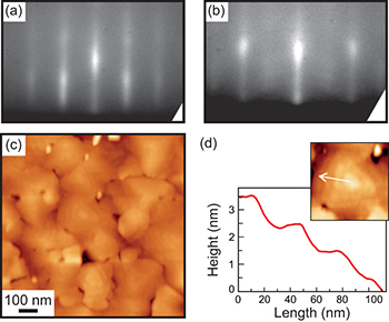
Fig. 1: (Color online) (a) RHEED image of a 59.4 nm thick Cr0.26Sb1.74Te3 film recorded at the end of growth along the [ ] azimuth of the c-plane sapphire substrate. A streaky pattern is visible, indicative of 2D growth. (b) RHEED taken along the
 ![$[11\bar{2}0]$](https://content.cld.iop.org/journals/0295-5075/115/2/27006/revision1/epl18023ieqn17.gif) azimuth. These RHEED patterns are separated by a substrate rotation of 30°. (c) AFM of grown film showing threefold symmetric spiral growth with quintuple layer steps expected from Sb2Te3. (d) Line scan across one of the triangular growth features, indicating quintuple layer steps of ∼1 nm in height. The position of the line scan is shown in the inset to (d).
azimuth. These RHEED patterns are separated by a substrate rotation of 30°. (c) AFM of grown film showing threefold symmetric spiral growth with quintuple layer steps expected from Sb2Te3. (d) Line scan across one of the triangular growth features, indicating quintuple layer steps of ∼1 nm in height. The position of the line scan is shown in the inset to (d).
Download figure:
Standard imageStructural characterization
Rutherford back-scattering spectrometry (RBS) was used for the accurate determination of the doping concentrations. It is found that the incorporated level of Cr dopant follows the expectation based on the in situ measurement of beam fluxes. X-ray diffraction (XRD), x-ray reflectometry (XRR), and rocking curves were obtained using a Bruker D8 diffractometer using incident Cu-Kα1 radiation. XRD measurements provide a strong indication of the crystal quality and phase of the grown film. The c-axis lattice parameters are extracted from the measured data using a Bragg's law fit to the peak positions of the observable (00l) order reflections. All films were grown to the same nominal thickness with varying concentrations of Cr dopant.
The XRR data (cf. fig. 2) were fitted using a three-layer model in the GenX package [18] to account for the grown nucleation layer and any reduced filling factor towards the sample surface. The thicknesses used for each of the three layers may be considered accurate in their total thickness, but have a greater degree of uncertainty in their individual thicknesses. This is due to the scattering length density varying only slightly between each layer to accommodate the Cr dopant or lower filling factor towards the surface. This means very little contrast for x-rays between the layers so that any change in layer thicknesses that leaves the total thickness unchanged creates a small change in the model fitting. Due to this, it makes little sense to quote in detail the interfacial mixing between each layer. Instead, the calculated roughness parameters are stated as a total interfacial roughness (RMS of all interfacial values) plus the surface roughness. The key parameters from the model fitted to the measured XRR data are shown in table 1.
Fig. 2: (Color online) XRR plots showing the measured data (colored dots) and fitted film structure (colored lines) for films with a Cr concentration of  , 0.26, and 0.42, as indicated in the legend. The intensities have been normalized to the maximum intensity, and offset in increments of 10 for clarity. The magnitude of the scattering vector, Q, normal to the surface is given by
  , with λ the wavelength of the x-rays and θ the angle of incidence. The inset shows a diagram of the three-layer model used for the fit is shown inset.
Download figure:
Standard imageTable 1:. Fitted parameters to the simulated model of the XRR measurement depicted in fig. 2. A representation of the film structure used in the model is shown as inset to that figure. Errors are computed based on 95% confidence bands of the relevant fit parameter. The given concentrations are from RBS results according to the nominal stoichiometry CrxSb2−xTe3.
 |
Layer thickness (Å) | Roughness (Å) | |||
|---|---|---|---|---|---|
| t1 (Sb2Te3) | t2 (CrxSb2−xTe3) | t3 (CrySb2−yTe3) | Interfacial | Surface | |
| 0.15 | 5.0 ± 1.2 | 600.550 ± 0.001 | 37.575 ± 0.001 | 18.96 ± 0.01 | 75.0 ± 1.0 |
| 0.26 | 5.47 ± 0.6 | 557.47 ± 0.2 | 31.06 ± 2.1 | 13.73 ± 1.0 | 50.00 ± 1 |
| 0.42 | 8.537 ± 0.001 | 603.19 ± 0.01 | 8.261 ± 0.004 | 13.33 ± 0.01 | 24.65 ± 0.01 |
It is clear from the measured diffraction spectra (fig. 3) that the grown films are well ordered, with the c-axis parallel to the surface normal of the sample. For increasing Cr doping concentration a reduction in the c-axis lattice parameter from 30.458 Å for undoped Sb2Te3 to 30.395 Å  , 30.308 Å
  , and 30.127 Å
  for the doped samples is observed, consistent with the idea of substitutional doping with an element with smaller ionic radius. This reduction of the lattice parameter was similarly observed for the analogue system CrxBi2−xSe3 [16,17], where it was ascribed to a contraction of the Cr-Se bond length compared with the Bi-Se bond length when substituting on the Bi site.

Fig. 3: (Color online) XRD for CrxSb2−xTe3 films with varying Cr doping concentration. Gray dashed vertical lines show the peak positions of undoped Sb2Te3. There is a clear shift of the peak positions towards higher angles (smaller c-axis lattice constants) as a function of increasing Cr doping.
Download figure:
Standard imageMagnetometry
The magnetic properties of the grown films were investigated using superconducting quantum interference device (SQUID) magnetometry, magneto-transport, and PNR. Measurements of the magnetization M as a function of the applied field H, and the temperature dependence of the magnetization, M(T), were carried out in a Quantum Design MPMS XL and SQUID VSM, respectively. Magneto-transport measurements were performed in a 9 T cryostat with a base temperature of 1.5 K and the PNR measurements on the PolRef beamline at the ISIS Neutron and Muon Source (Rutherford Appleton Laboratory, UK). SQUID measurements were made of the field dependence, M(H), and temperature dependence, M(T), of a selection of CrxSb2−xTe3 thin films with varying Cr doping levels. All samples are ferromagnetically ordered at low temperature, with the easy axis of magnetization parallel to the c-axis (out-of-plane) and the hard axis in the  -plane. Field-dependent magnetization data have been processed using a linear fit to the high-field region to subtract the diamagnetic contribution of the sapphire substrate. The data shown in fig. 4 is of the film only, with the substrate contribution removed. The units of the vertical axis are scaled using the sample volume and Cr concentration, as measured by RBS.
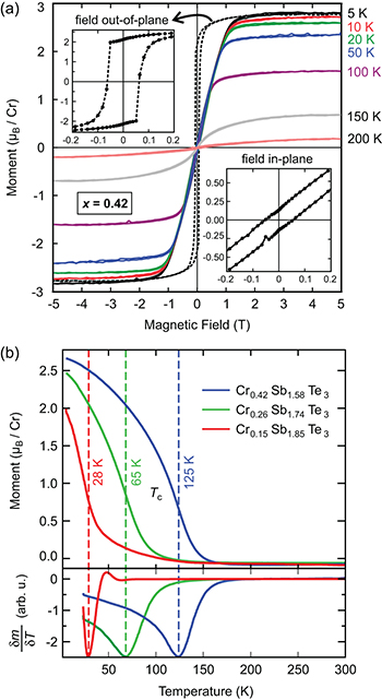
Fig. 4: (Color online) (a) Magnetization curves, M(H), of a Cr0.42Sb1.58Te3 thin film measured at varying temperatures with the field in-plane (solid lines) and at 5 K in an out-of-plane field (dashed line). The insets show the behavior at small fields at 5 K for the field applied out-of-plane (top left) and in-plane (bottom right), respectively. (b) Temperature dependence of magnetization M(T) of samples of varying Cr concentration measured whilst cooling in a 20 mT applied out-of-plane field. The observed transition temperatures, obtained from the minima of the derivative  shown at the bottom, are marked by dashed lines.
Download figure:
Standard imageThe full set of measurements obtained from SQUID magnetometry is shown in fig. 4. Figure 4(a) shows temperature-dependent M(H) loops for the Cr0.42Sb1.58Te3 sample with the field applied parallel and perpendicular to the c-axis, respectively. The saturation magnetization is (2.8 ± 0.2) μB/Cr, the stated uncertainty is dominated by statistical error in the determination of film volume. The volume was obtained from the XRR thickness and measurement of the area of the substrate. Further, the uncertainty of determining the doping concentration from RBS results is taken into account. The saturation magnetization is less than the theoretical Hund's rules value of 3 μB/Cr. However, for Cr-doped Bi2Se3 the hybridization between the Cr-d and Se-p orbitals increases the covalency, effectively reducing the oxidation state of the Cr dopant [16], a similar effect may be anticipated in this system.
At  , all samples show soft ferromagnetic behavior. The saturation magnetization is dependent on the doping concentration and reaches
  ion. M(T) measurements were taken whilst cooling in a field of 2 mT applied in a hard-axis direction in the plane, as shown in fig. 4(b). The diamagnetic contribution to the signal was removed. All samples show a clear paramagnetic to ferromagnetic transition, with the transition temperature
  varying strongly with doping concentration.
  is identified from the smoothed first derivative of each curve (fig. 4(b), bottom) and varies between 28 K for the lowest doping concentration, up to 125 K for the highest doping concentration. Note that no impurity phases are detected for Cr0.42Sb1.58Te3 in XRD.
Electric transport studies
Magneto-transport measurements were carried out on a 60 QL thick Cr0.42Sb1.58Te3 sample. Photolithography and argon ion milling were used to define a microscale Hall bar of dimensions  , followed by 20/80 nm thick Ti/Au Ohmic contacts deposited using a standard lift-off process as shown in the inset to fig. 5. The device was then packaged and measured using a standard AC four-terminal setup with an excitation current of
  at a frequency of 33 Hz. The temperature-dependent sheet resistance Rs was measured at zero magnetic field and is plotted in fig. 5. In the range from room temperature to 25 K, the bulk resistance shows a steep decrease with decreasing temperature. This is characteristic for metallic behavior with a positive temperature coefficient, an effect widely seen in TIs [19,20]. The decrease can be attributed to decreased phonon scattering. However, the resistance then goes up with further decreasing temperatures down to 15 K, consistent with semiconducting behavior. This increase can be explained by the freezing out of bulk conduction band carriers into an impurity band [21]. Finally, the resistance levels out and becomes largely temperature-independent as the temperature is further reduced to 1.5 K. This region is most likely to be dominated by a combination of surface conduction and impurity band conduction [22].
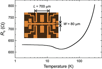
Fig. 5: (Color online) Sheet resistance  vs. temperature for a 60-QL-thick Cr0.42Sb1.58Te3 sample grown on c-plane sapphire. The inset shows the Hall bar structure with length
  and width
  .
.
Download figure:
Standard imageFigure 6 shows the field dependence of the Hall resistance Rxy at a range of temperatures. The main objective was to investigate the magnetic properties through the anomalous Hall effect (AHE). Clear hysteresis loops show that the film is in a long-range–ordered ferromagnetic state, consistent with the SQUID data shown in fig. 4. Similar behavior has been observed in Cr and V-doped (BixSb1−x)2Te3 [4,5,23–25]. In a 2D system, the total Hall resistance is given by  , where R0 is the (ordinary) Hall coefficient, which is inversely proportional to the Hall density, M(H) is the magnetization component perpendicular to the film, and RA is the anomalous Hall coefficient affected by intrinsic and extrinsic scattering mechanisms [26,27]. In the high-magnetic-field limit the Hall resistance component dominates and in the low-magnetic-field region, the anomalous Hall component dominates. Therefore, the slope of Rxy at high fields determines the two-dimensional Hall density,
  , which is calculated to be
  at 1.5 K, comparable to the values reported in refs. [5,23,24] for very thin films. A low carrier density is required to achieve the charge neutrality point by compensation doping with Bi [28]. An estimate for the transition temperature,
  , was obtained by determining the temperature at which the AHE-related part of resistance,
  , became non-zero, as plotted in the inset to fig. 6. We obtain a
  in agreement with the value obtained from SQUID magnetometry (cf. fig. 4(b)).
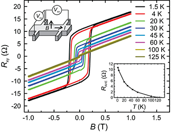
Fig. 6: (Color online) Field dependence of Rxy in a range of temperatures showing the AHE. The inset shows RH reducing as the temperature increases, reaching a value close to zero at 125 K.
Download figure:
Standard imagePolarized neutron study
PNR was used to extract the structural and magnetic depth profile of the  and 0.42 samples at both 5 and 300 K. A magnetic field of 0.65 T was applied parallel to the neutron spin, in the plane of the sample. Reflectivity curves for the two neutron-spin eigenstates were measured without polarization analysis. Model fitting was carried out using an optical transfer matrix approach [29] and a differential evolution fitting algorithm using the GenX package [18]. The reflectivity data and spin asymmetry at 5 K for both samples are shown in fig. 7(a), (b). Figure 7(c) demonstrates the structural and magnetic depth profile for the
  sample.

Fig. 7: (Color online) PNR for the  and 0.42 samples in an applied field of
  at a temperature of 5 K. The normalized reflectometry of both samples is shown in (a) with the
  data being offset by 10−2. (b) Spin asymmetry as a function of the wave vector transfer. The solid line is the best-fit calculation for the model described in the text. (c) Model of the SLD at 5 K for the
  , layered thin-film system, consisting of substrate (dark gray), Sb2Te3 buffer layer (yellow), a Cr-doped layer and top layer (light gray).
Download figure:
Standard imageA variety of fits were attempted allowing the layer thickness, density, roughness, and Cr concentration to vary. In order to test for an inhomogeneous doping profile, we performed fits where the Cr-doped layer was divided into several layers where saturation magnetization was allowed to vary as well. For the  sample, the best fits were obtained using a model similar to the structural model for the XRR data, consisting of three separate layers: the pure Sb2Te3 buffer layer and two CrxSb2−xTe3 layers with differing Cr concentrations. For the
  sample, the best fits were obtained using a two-layer model consisting of the undoped buffer layer and a single CrxSb2−xTe3 layer. The buffer layer has a thickness of 4.8 nm and 6.5 nm for the
  and
and  samples, respectively, and has a low scattering length density (SLD). The magnetization of the buffer layer was allowed to vary but each model shows this layer has no magnetic moment.
The roughness of the interface between the substrate and buffer layer was below the measurable limit for both samples. The interface between the buffer layer and the doped layer is less sharp and transitions are gradually over ∼3 nm for both sample models. There is also a ∼3 nm wide transition region between the doped layer and the top layer of the  sample. Both models give a surface roughness of ∼2 nm.
The best-fit model for the  sample had a top layer thickness of 4.3 nm and a reduced SLD relative to the bulk of the film. The magnetization of this layer was also allowed to vary to allow for the possibility of a different Cr moment; however, no magnetization was favored.
Apart from layer mixing at the interface, the majority of each sample consists of a CrxSb2−xTe3 layer with a single Cr concentration and with thicknesses of 59 nm and 54 nm for the  and
and  samples, respectively. The densities are within 6% of the nominal values [30]. The Cr concentration of the interfacial transition region was fixed to the value determined by RBS measurements for both samples. The best-fit models suggest a uniform magnetization profile with a gradual transition between the buffer layer and the doped layer, as well as a gradual decay in magnetization up to the sample surface. For both samples the estimated moment was found to be
  , which is in agreement with SQUID results obtained at a field of 0.65 T and a temperature of 5 K. The gradual decay in magnetization up to the sample surface shows no enhancement of the magnetization in the surface region. We can conclude that there is no near-surface modification to the polarization present in our results.
Summary and conclusions
We have demonstrated that Cr-doping of Sb2Te3 thin films is possible up to a concentration of  without a significant loss of structural quality or the formation of secondary phases using a complementary multi-technique approach. Increased doping of Sb2Te3 leads to a decreased c-axis lattice constant as expected in a substitutional doping scenario with a smaller diameter ion. A magnetic saturation moment of
  was determined by SQUID for the
  sample. Magneto-transport measurements carried out on the
  sample demonstrate a carrier concentration of
  at 1.5 K and a transition temperature obtained from the AHE loops consistent with the value derived from SQUID measurements of 125 K. PNR shows that the films exhibit homogeneously distributed magnetic moments with no evidence of an enhanced surface magnetic layer. The moment of the Cr ions distributed throughout the samples was found to be in agreement with SQUID magnetometry measurements carried out at the same field and temperature. The magnetic ordering temperature found for high structural, electric and magnetic quality films is ∼125 K, bringing us closer to the realization of novel topologically driven phases at more accessible temperatures (> 77 K).
Acknowledgments
This work arises from research funded by the John Fell Oxford University Press Research Fund. We thank ISIS for neutron beamtime (RB1510161), Diamond Light Source for AFM, SQUID, and XRD access, and RCaH for their hospitality. LJC-M and LBD acknowledge financial support from EPSRC. LBD acknowledges financial support from the Science and Technology Facilities Council (UK) and AS from the Cambridge Commonwealth Trust.