Abstract
In this study, deep-ultraviolet 280-nm-wavelength light-emitting diodes (DUV LEDs) with a nanopatterned sapphire substrate (NPSS) were fabricated using a nanoimprint lithography process. The output power of these flip-chip (FC) DUV LEDs was measured and analyzed in a ray-tracing simulation using NPSSs: cones with diameters of 2.5 μm (LED1), 400 (LED2) and 200 nm (LED3) as well as holes with diameters of 350 (LED4) and 750 nm (LED5). For comparison, a mirror for the c-plane FC DUV LEDs was introduced by coating Ni/Au and Al thin films. With the injection current at 350 mA, the output powers of the c-plane, LED1, LED2, LED3, LED4, and LED5 were 13.38, 14.68, 20.05, 16.79, 15.74, and 18.93 mW, respectively. The LED2 efficiency improved 49.9% compared with mirror LED and the result was consistent with ray-tracing simulation.
Export citation and abstract BibTeX RIS

This is an open access article distributed under the terms of the Creative Commons Attribution 4.0 License (CC BY, http://creativecommons.org/licenses/by/4.0/), which permits unrestricted reuse of the work in any medium, provided the original work is properly cited.
In 1993, the first blue light-emitting diodes (LEDs) were fabricated using InGaN/GaN film materials,1 resulting in extensive research on GaN-based materials. By varying the Al and In content to tune the AlGaInN bandgap,2,3 light emission wavelengths from green to ultraviolet (UV) can be obtained.4 Therefore, LED devices have broad applications and market opportunities, for example, displays, lighting, signage, and medical treatment.
Deep ultraviolet (DUV) LEDs with wavelengths of 250–300 nm5–9 exhibit small volumes, are nontoxic, and have longer lifespans compared with traditional mercury lamps. These LEDs can be used in disinfection, air and water purification, biochemical inspection, and optical communication.1–5 In recent years, improved AlGaN-based DUV LEDs have been developed. The epilayer quality can considerably affect the internal quantum efficiency (IQE). The external quantum efficiency (EQE) of DUV LEDs is low because of their low light extraction efficiency (LEE), which is insufficient for most practical applications.6–11 Currently, LG Innotek has reported the best LEE. In LG Innotek's LEDs, wafer bonding and laser lift-off technology are combined for fabricating thin-film and vertical-type DUV LEDs. The fabrication process is difficult, and the yield is limited because laser lift-off for DUV LEDs is difficult. Compared with vertical-type DUV LEDs, the fabricated processing of flip-chip (FC) LEDs is simpler, and the fabricated yield is higher. However, the technical problems in fabricating short-wavelength LEDs should be addressed to increase the LEE of FC LEDs.
Currently, the majority of DUV LED epilayers are grown on flat sapphire substrates, and FC packages with flat emission surfaces are used. However, this can result in the inability of light to escape into the air because of total light reflection. Patterned sapphire substrates have been widely used in epitaxial growth for blue and green GaN-based LEDs and offer higher epilayer quality and superior light extraction enhancement about 46% comparing to flat sapphire substrates. However, fabrication of AlGaN on a patterned sapphire substrate is difficult because of the low diffusion rate for of the Al source during metal organic chemical vapor deposition (MOCVD). In this study, DUV LEDs were fabricated on flat sapphire substrates. However, the patterns were produced on the back side of the sapphire substrates. The FC DUV LEDs with nanopatterned sapphire substrates (NPSSs) were fabricated through a nanoimprint lithography process to maximize the EQE of the devices. The EQE of the DUV LEDs was analyzed using ray-tracing simulation for the FC DUV LEDs with NPSSs of a variety of depths, sizes, and spacing. Ni/Au and Al thin films were introduced as a transparent contact layer and a mirror for the DUV LEDs, respectively. The nanopatterns' effect on the DUV LEDs is analyzed in this paper.
Experimental
Epitaxial structures were fabricated on c-plane sapphire substrates through MOCVD. DUV LEDs emitting 280-nm light were fabricated on flat c-plane sapphire substrates with a 2-μm-thick undoped Al0.75Ga0.25N template, a Si-doped 2.5-μm-thick n- Al0.75Ga0.25N layer, multiple quantum wells consisting of nine pairs of Al0.5Ga0.5N/Al0.42Ga0.58N multi-quantum wells, a 40-nm-thick electron blocking layer, and a 100-nm-thick Mg-doped p-Al0.75Ga0.25N layer. Then, 3-nm-thick p+-GaN was grown for the o contact layer. After epitaxial growth, a mesa was etched to the n- Al0.75Ga0.25N layer through inductively coupled plasma reactive ion etching. Then, Ti (35 nm)/Al (75 nm)/Ti (15 nm)/Au (90 nm), and Ni (5 nm)/Au (5 nm) were deposited using an e-gun to serve as the n-pad and p-pad, respectively, and subsequently annealed at 500°C for o contact. Furthermore, Al thin films were introduced as mirrors for the DUV LEDs. The UV LED chip size was 1 mm × 1 mm. Finally, the FC die-attaching process was implemented on the AlN substrate to finish the traditional FC DUV LED (mirror LED). With regard to the nanopatterns, 2.5-μm-diameter cone LEDs with 2.8-μm pitch (LED1), 400-nm-diameter cone LEDs with 900-nm pitch (LED2), 200-nm-diameter cone LEDs with 730-nm pitch (LED3), 300-nm-diameter hole LEDs with 750-nm pitch (LED4), and 150-nm-diameter hole LEDs with 350-nm pitch (LED5) were fabricated using a nanoimprint lithography process, and an NPSS structure was obtained through dry etching before the DUV LED processing. A schematic of the nanoimprinted DUV LED device is presented in Fig. 1.
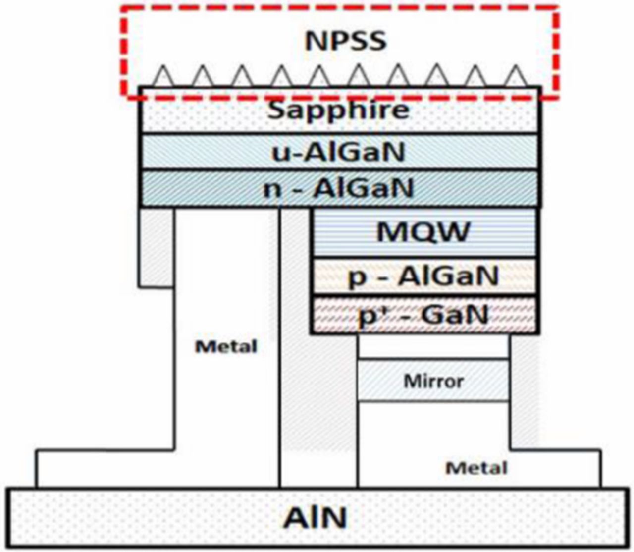
Figure 1. NPSS DUV LED device structure.
Results and Discussion
To evaluate the nanopattern's effect on the EQE, a geometrical model was built in SolidWorks, and the radiant intensity was analyzed using a simulation in TracePro software. The simulation parameters included a chip size of 10 mil × 10 mil made by c-plane sapphire with 400-μm thickness, light source of 280-nm in wavelength, sapphire refractive index n2 = 1.8, and air refractive index of 1. The construction model contains that light source of 280-nm was in the center of a circle with radius 15 mil and was also inside the chip. So, the light can emit from the chip surface and was gathered by the surface of a hemisphere. The surface structures of the sapphire contained a c-plane and LEDs 1–5. Table I lists the geometric parameters of LEDs 1–5. The simulation results are presented in Figs. 2 for these surface structures. The radiant intensity was 0.32, 0.40, 0.46, 0.44, 0.41, and 0.46 W/sr for c-plane, LED 1, LED2, LED3, LED4, and LED5, respectively. The radiant intensity was higher for the DUV LEDs with a patterned substrate than the FC DUV LEDs with a flat sapphire. According to the simulation results, changing the substrate surface structure can improve the radiant intensity and LEE. The simulation result could be used to verify the experimental result.
Table I. Related parameters of the cone-shaped LEDs.
| Parameter\Device | LED1 | LED2 | LED3 | LED4(hole) | LED5(hole) |
|---|---|---|---|---|---|
| 2R (nm) | 2500 | 400 | 200 | 300 | 150 |
| P (nm) | 2800 | 900 | 730 | 750 | 350 |
| H (nm) | 1500 | 290 | 210 | 290 | 250 |
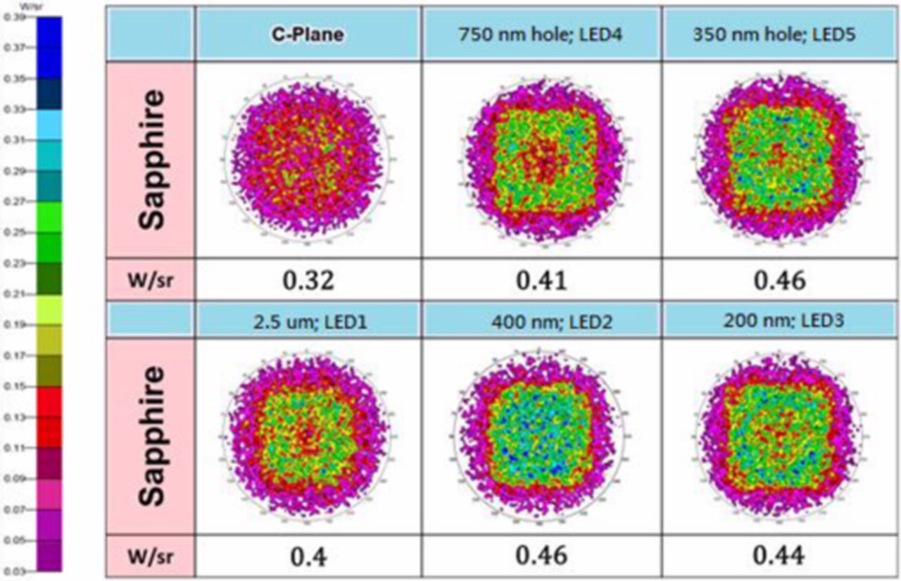
Figure 2. TracePro simulation of different NPSS structures.
Fig. 3 depicts scanning electron microscopy (SEM) images of various NPSSs fabricated using the nanoimprint lithography process. To understand how light emitted from the patterns, measurement of patterns was conducted by top view at 45° tilt, top view at 0° and cross-section view. Figs. 3a–3c present SEM images of the nanoimprinted 2.5-μm diameter on the sapphire substrate of DUV LEDs. The cone is 2.57 μm in diameter, with pitch of 2.8 μm and depth of 1.5 μm. Figs. 3d–3f present SEM images of nanoimprinted 400-nm cones on the sapphire with pitch of 900 nm and 290-nm depth. Figs. 3g–3i present SEM images of nanoimprinted 200-nm-diameter cones on the sapphire substrate with pitch of 730 nm and 210-nm depth. To evaluate the LEE factors, hole patters were also prepared. Figs. 3j–3l present SEM images of nanoimprinted 750-nm holes with 290-nm depth on an NPSS for a DUV LED. The hole diameter in the bottom is 300 nm with a hole-to-hole distance of 750 nm and 290-nm depth. Figs. 3m–3o present SEM images of nanoimprinted 350-nm holes with 250-nm depth in a sapphire substrate. At the bottom, the hole diameter was 150 nm, with hole-to-hole distance of 350 nm. The SEM images demonstrate that the nanopatterns were fabricated on the emission side of the sapphire substrate through the combination of nanoimprint lithography technology and dry etching.
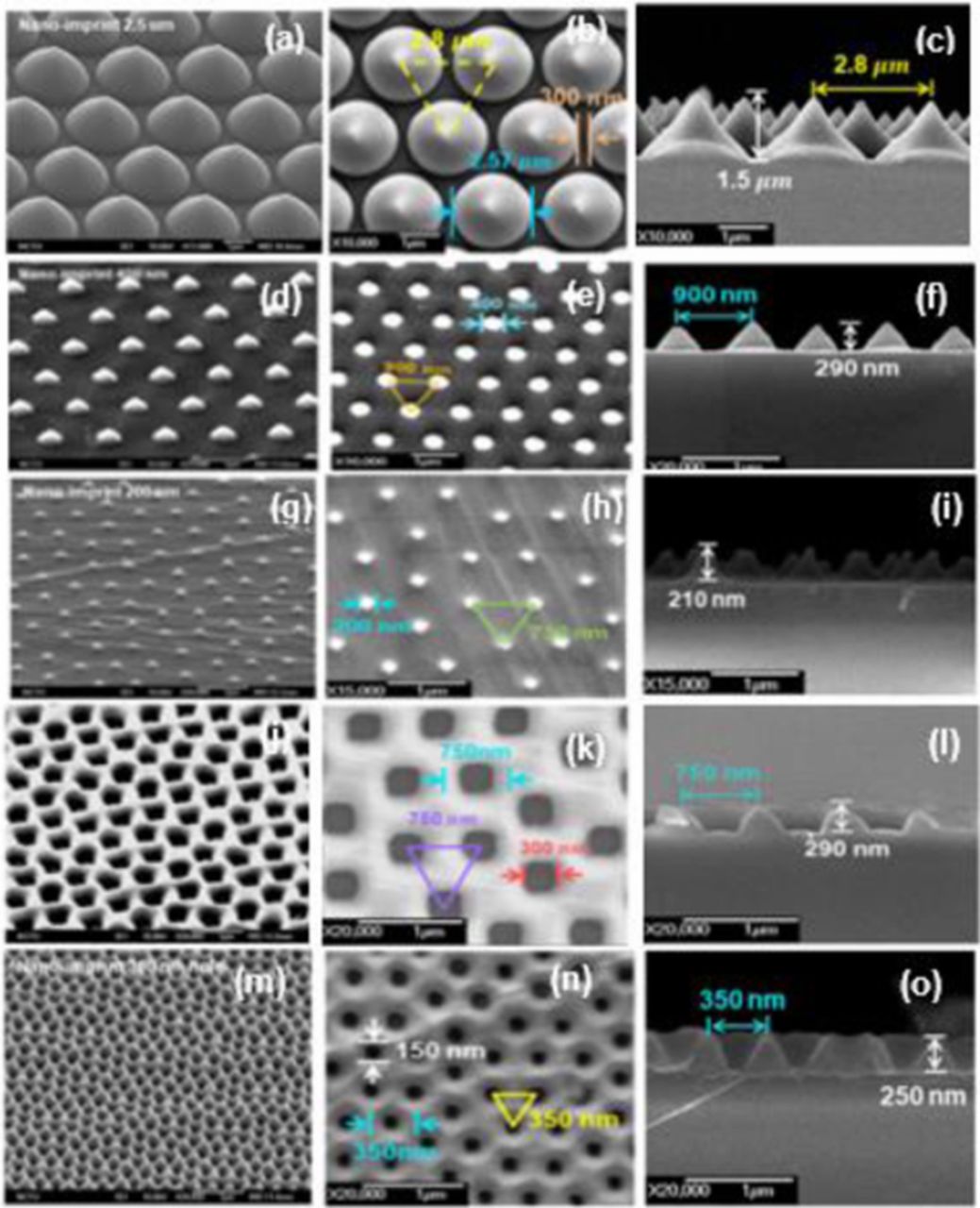
Figure 3. SEM images of nanoimprinted cones patterns with (a)–(c) 2.5-μm, (d)–(f) 400-nm, (g)–(i) 200-nm diameters, and hole patterns with (j)–(l) 750-nm, (m)–(o) 350-nm diameters in NPSS structures.
Fig. 4a shows the current–voltage characteristic and electroluminescence (EL) spectra for the FC DUV LED. Because the nanopatterns were imprinted on sapphire substrates, they did not affect the electrical properties or EL. The voltages were approximately 5.5 and 9 V for current at 20 and 350 mA, respectively. The EL peak was approximately 285 nm with the injection current at 350 mA.
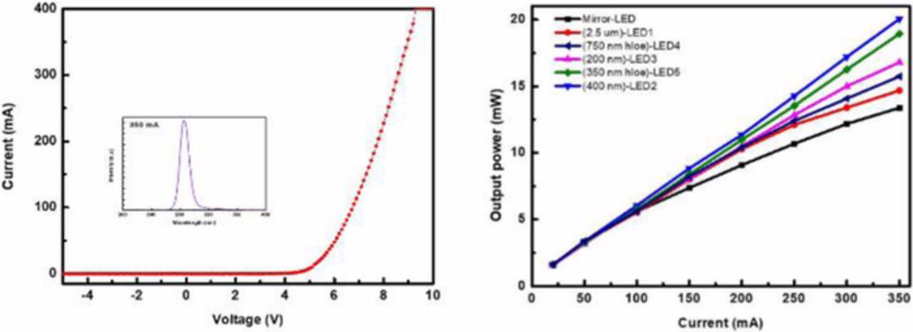
Figure 4. (a) I–V characteristic and electroluminescence (EL) spectra for the typical FC DUV LEDs and (b) L–I characteristic curve of the FC DUV LEDs.
The main concern of this study was the effect of nanopatterns on the light output power of UVC LEDs. Fig. 4b shows the light output power as a function of the injecting current (L–I) characteristics of the c-plane as well as LEDs 1–5. The LEDs were easily to burn out as the injected current was higher than 350 mA. In order to obtain all properties of UVC LEDs for comparison, here, we only measure properties under 350 mA. The output powers of the DUV LEDs with these structures were 1.58, 1.57, 1.62, 1.57, 1.61, and 1.61 mW measured at 20 mA for the mirror LED and LEDs 1–5, respectively. When the injection current was increased to 350 mA, output powers of the mirror LED, LED1, LED2, LED3, LED4, and LED5 were 13.38, 14.68, 20.05, 16.79, 15.74, and 18.93 mW, respectively. It was found that the thermal effect is serious on the L-I-V measurements as the high current injection. This is why the measurement was measured below 350 mA. Even below 350 mA, the UVC LED with mirror presented the early saturation as compared with others LED did. The nanoimprinted 400-nm LED exhibited the highest illumination intensity, and its efficiency was a 49.9% improvement over the mirror LED. This result is consistent with the TracePro simulation; that is, the 400-nm imprint had increased the radiant intensity and LEE. This result occurred because 400 nm is approximately mλ/2(n), which is ideal for allowing more light outgoing into air. This result agrees well with the simulation shown in Fig. 2. As in Fig. 2, it shows many light wavelengths (blue color) can be output by the 400-nm-diameter nanopattern. On the other hand, it was found that the thermal effect is serious on the L-I-V measurements as the high current injection. This is why the measurement was measured below 350 mA. Even below 350 mA, the UVC LED with mirror presented the early saturation as compared with others LED did.
The wall plug efficiency (WPE) of the FC DUV LEDs is shown in Fig. 5. With an operating current at 20 mA, the WPEs of the mirror LED and LEDs 1–5 were 1.41%, 1.44%, 1.47%, 1.40%, 1.04%, and 1.32%, respectively. When the current was increased to 350 mA, the WPEs of the mirror LED, nanoimprinted 2.5-μm, 400-nm, and 200-nm cone LEDs and nanoimprinted 750-nm and 350-nm hole LEDs were 0.36%, 0.45%, 0.61%, 0.49%, 0.42%, and 0.55%, respectively. Based on this result, the WPEs of the nanoimprinted 2.5-μm, 400-nm, and 200-nm cone LEDs and nanoimprinted 750-nm and 350-nm hole LEDs were improved 16.7%, 69.4%, 36.1%, 25.0%, and 52.8% over the mirror LED in the high-current condition. The WPE of the nanoimprinted 400-nm LED was the highest. The nanoimprinted 350-nm hole LED presented the second-best performance.
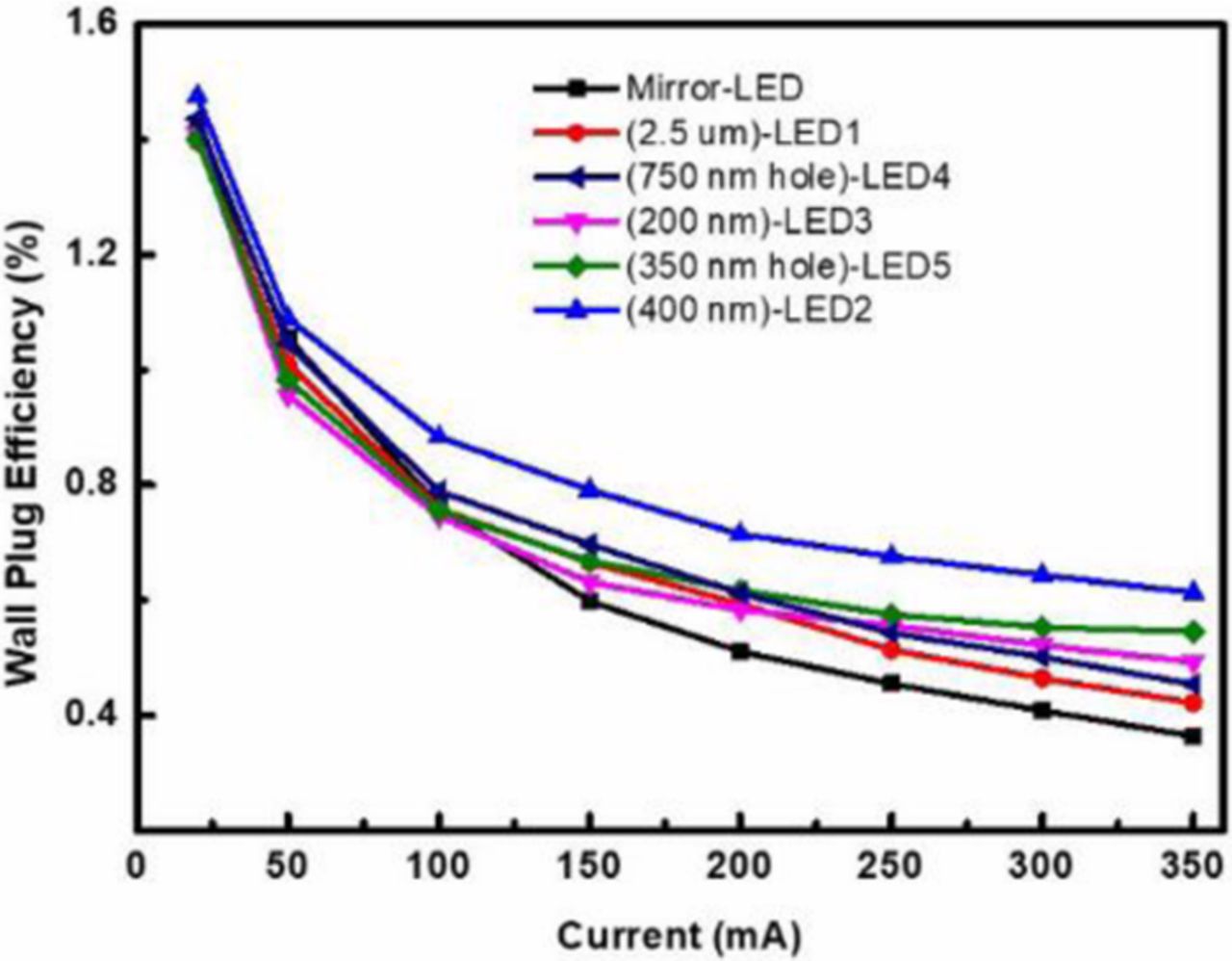
Figure 5. WPE–I characteristics of the FC DUV LEDs.
The EQE of the FC DUV LEDs was calculated using the following equation:12
![Equation ([1])](https://content.cld.iop.org/journals/2162-8777/9/1/015005/revision1/d0001.gif)
where Eph is the photon energy, Vf is the device's forward voltage, and q is the electron charge.
We can calculate the EQE using Eq. 1 with Eph = 4.43 eV at 280 nm when operating current is at 20 mA, as shown in Fig. 6. The EQEs of the mirror LED and LEDs 1–5 were 1.78%, 1.77%, 1.82%, 1.77%, 1.77%, and 1.81%, respectively. When the current was increased to 350 mA, the EQEs were 0.86%, 0.95%, 1.29%, 1.08%, 1.02%, and 1.22%. The EQE of the nanoimprinted 400-nm LED was the highest, and its result was consistent with TracePro simulation because the nanopattern changed the critical angle and enhanced the external LEE. However, an emitting surface with a hole pattern measuring 150 nm in diameter at the bottom with a hole-to-hole distance of 350 nm can also yield good EQE, meaning that not only convex patterns but also concave patterns can enhance EQE if the pattern dimension is appropriately matched with the emission wavelength, such as LED2 and LED5.
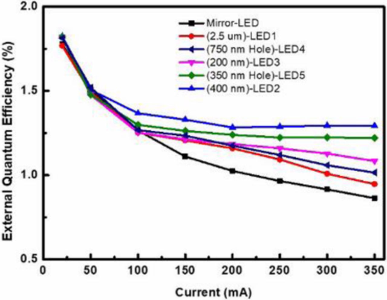
Figure 6. EQE–I characteristics of the FC DUV LEDs.
Conclusions
In this study, FC DUV LEDs with NPSSs were fabricated through nanoimprint lithography to improve the EQE of LED devices. LEDs with nanoimprinted 2.5-μm, 400-nm, and 200-nm cones and 750- and 350-nm holes exhibited EQEs 10.4%, 49.8%, 25.5%, 18.6%, and 41.8% higher than that of a traditional FC mirror DUV LED. For the first time, FC DUV LEDs with optimized NPSSs were nanoimprinted with 400-nm LEDs for EQE improvement of 49.8% over a conventional mirror LED. The result is consistent with a ray-tracing simulation due to the decreased internal total reflection on the interface between the sapphire and air. However, an emitting surface with a hole pattern measuring 150 nm in diameter at the bottom with a hole-to-hole distance of 350 nm can also yield good EQE, meaning that not only convex patterns but also concave patterns can enhance EQE if the pattern dimension is appropriately matched with the emission wavelength.
Acknowledgments
This study was financially supported by the Research Team of Photonic Technologies and the Intelligent System at NCTU within the framework of the Higher Education Sprout Project by the Ministry of Education in Taiwan and the Ministry of Science and Technology (MOST) and by Hsinchu Science Park, Taiwan, R.O.C., under Grants MOST (107-2221-E-009-117-MY3, 107-2262-E-009-018-CC2, 107-2218-E-009-056); Hsinchu Science Park (HSP) (106A03). Thank LUCEMITEK CO., LTD in Taoyu, Taiwan for the nano patterns fabrication.
ORCID
Ray-Hua Horng 0000-0002-1160-6775