
Abstract
The recent experimental synthesis of the monolayer γ-GeSe, characterized by its unique Mexican-hat band dispersion, has attracted considerable research interest. However, the exploration of band gap engineering in bilayer γ-GeSe and γ-SnSe through the application of strain and electric fields remains under-investigated. In this study, we demonstrate that both strain and electric fields are effective methods for band gap engineering in bilayer γ-GeSe and γ-SnSe. We have discovered that strain can not only tune the band gap but also induce a transition from an indirect to a direct band gap. Furthermore, it is observed that the band gap of bilayer γ-GeSe and γ-SnSe can be modulated by an electric field, potentially leading to a transition from semiconductor to metal. Our findings suggest that band gap engineering via strain and electric fields is a promising approach for designing nanoelectronic and optoelectronic devices based on bilayer γ-GeSe and γ-SnSe.
Export citation and abstract BibTeX RIS

Original content from this work may be used under the terms of the Creative Commons Attribution 4.0 licence. Any further distribution of this work must maintain attribution to the author(s) and the title of the work, journal citation and DOI.
1. Introduction
Two-dimensional (2D) layered materials have attracted considerable attention due to their exceptional fundamental physical properties and their immense potential in device applications. The experimental exfoliation of graphene ignited research efforts in 2D layered materials[1–5]. Subsequently, 2D transition metal dichalcogenides (TMD) [6–8] and black phosphorene [9–12] have been extensively researched, particularly for their potential applications in ultra-thin transistors. More recently, the layered 2D MoSi2N4 family has been under extensive study, attributed to their high carrier mobility and excellent air stability [13–26].
Band gap engineering is crucial in the fabrication of devices based on semiconducting 2D layered materials. Previous studies have shown that strain can effectively modulate the electronic properties of these materials [27–34]. Another approach to achieve band gap engineering involves applying an electric field to semiconducting 2D layered materials, which has been proven effective in tuning the band gap [35–43]. These methods of band gap engineering pave the way for the development of devices based on 2D layered materials. Furthermore, emerging 2D materials and their heterostructures demonstrate promising properties for thermal and optical applications [44–47].
Very recently, a new phase of group IV monochalcogenides featuring two merged buckled honeycomb sub-lattices, known as γ-GeSe, was theoretically predicted and experimentally synthesized [48, 49]. The bulk form of γ-GeSe exhibits remarkably high electrical conductivity, reaching 3 × 10⁵ Sm−1. When reduced to a monolayer, γ-GeSe transforms into an indirect band gap semiconductor, characterized by a Mexican-hat (MH) like energy band dispersion at the valence band maximum near the Γ point. This unique MH band often leads to exceptional electronic properties, primarily due to the band edge Van Hove singularity. Extensive research has been conducted to explore the exceptional properties of γ-GeSe [50–52]. Studies on the effects of strain and electric field on monolayer γ-GeSe have been undertaken to aid in nanoelectronic device design [53–55]. Nevertheless, to date, there is still a lack of studies focusing on the band gap engineering of bilayer γ-GeSe. Since bulk materials are less sensitive to strain and electric field effects, our study will primarily focus on bilayer γ-GeSe and γ-SnSe.
In this work, we investigate the effects of strain and external electric fields on the electronic band structure of bilayer γ-GeSe and γ-SnSe. We discover that both compressive and tensile strains can modify the band gap. This alteration in the band structure is attributed to changes in the Ge/Sn-Se bond length and the thickness of the bilayer induced by the strain. Furthermore, we find that the application of an external electric field can also tune the band gap. The charge redistribution caused by the electric field is identified as the underlying mechanism for this tuning of the band gap. Our findings suggest that bilayer γ-GeSe and γ-SnSe, with their strain and electric field-tunable electronic properties, could be promising candidates for the next generation of nanoelectronic and optoelectronic applications.
2. Methodology
In this study, density functional theory (DFT) first-principles calculations were employed to investigate the γ-GeSe and γ-SnSe bilayers under strain and external electric fields. We utilized the Vienna Ab initio Simulation Package (VASP) [56, 57] for geometry optimization and QuantumATK [58] to examine the electronic properties. A gamma-centered k-point mesh of 8 × 8 × 1 was used for the geometry optimization and 16 × 16 × 1 for the property calculations, both based on the Monkhorst–Packmethod [59]. The atomic force criterion for the geometry optimization was set at 0.01eV/Å. The generalized gradient approximation (GGA) with the Perdew–Burke–Ernzerhof form (PBE) [60] was selected for the exchange-correlation functional in the geometry optimization. For the accurate electronic structure of the bilayers, we employed the Heyd-Scuseria-Ernzerhof hybrid functional method (HSE) [61]. The DFT-D3 method with the Grimme scheme [62, 63] was adopted to account for the weak van der Waals interactions in the bilayers. To eliminate interactions from periodic images, a 20 Å thick vacuum layer was inserted between adjacent bilayers. Here, the excitonic binding energy (GW calculation) is not considered due to its high computational cost and our primary focus on the trends of electronic properties modulation by strain and electric field.
3. Results and discussion
Based on total energy calculations, we identified the most stable bilayer configuration with the lowest total energy, as depicted in figure 1(a). This finding is consistent with previous studies [52]. Our calculated lattice parameters for the γ-GeSe and γ-SnSe bilayers are a = 3.77 Å and 4.06 Å respectively, agreed well with previously calculated results for monolayers [48]. The calculated band structures of the γ-GeSe and γ-SnSe bilayers are presented in figure 1(b). As observed in the band structure, the interlayer interactions cause a splitting of the energy bands from the top and bottom layers, leading to a reduced band gap for both the γ-GeSe and γ-SnSe bilayers. The band gaps of the γ-GeSe and γ-SnSe bilayers are calculated to be 0.62 and 0.55 eV, respectively.
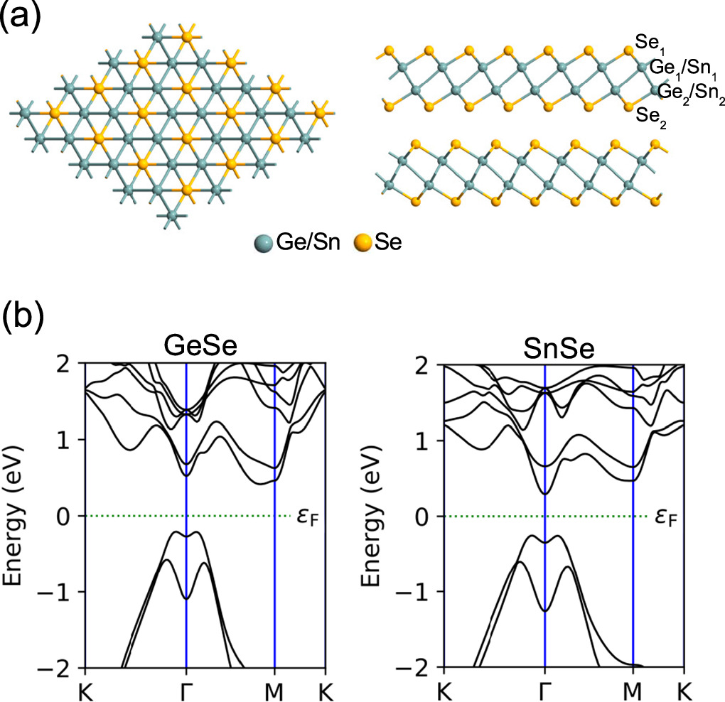
Figure 1. (a) Top and side view of bilayer γ-GeSe and γ-SnSe. (b) HSE band structure of bilayer γ-GeSe and γ-SnSe.
Download figure:
Standard image High-resolution imageStrain engineering can modulate the electron states of 2D materials, leading to changes in their electrical, magnetic, and optical properties. In this study, we employ biaxial strain to tune the energy band gap of the bilayer γ-GeSe and γ-SnSe. Strain (ε) is defined as ε = (a − a0)/a0 × 100%, where a and a0 represent the lattice parameters of the strained and unstrained bilayers, respectively. The evolution of the band structure with applied strain is shown in figure 2. Figure 3(a) displays the variation of the band gap as a function of applied strain for bilayer γ-GeSe and γ-SnSe. We observe that the band gap decreases monotonically with increasing tensile strain. However, with increasing compressive strain, the band gap initially increases and then decreases at around -2 % for the bilayer γ-SnSe. Nevertheless, both band gap of bilayer γ-GeSe and γ-SnSe can be reduced to zero at -4 % and -8 % of strain. It is also noted that strain can transition the band gap from indirect to direct at approximately 10 % tensile strain for both bilayer γ-GeSe and γ-SnSe. The projected band structures to the top and bottom layers, along with the partial charge density corresponding to the valence band maximum (VBM) and conduction band minimum (CBM) for bilayer γ-GeSe and γ-SnSe under −4/−8 % and 10 % strain, are presented in figures 3(b) and (c) to elucidate the strain-engineered electronic structure. From the projected band structure, it is evident that the VBM and CBM originate from both the top and bottom layers of the bilayer γ-GeSe and γ-SnSe, with a reduced band gap for both compressive and tensile strains. Notably, the bilayer γ-GeSe and γ-SnSe become direct band gap semiconductors at a 10 % tensile strain. In the partial charge density plots, we observe a predominance of s orbitals for the Ge/Sn atoms in the VBM and CBM under a compressive −4/−8 % strain. However, with a tensile 10 % strain, there is a greater presence of pz orbitals for the Ge/Sn atoms in the VBM and CBM. This can be attributed to the changes in bond length and thickness as a function of applied strain, as illustrated in figure 3(d). Under compressive strain, the bond length of Ge/Sn-Se decreases, strengthening the interaction between atoms and dispersing the energy bands more widely. Conversely, under tensile strain, the reduction in thickness enhances interlayer atomic interactions, also leading to a more dispersed band structure. Consequently, the band gap decreases due to these effects. This phenomenon is further supported by the stronger out-of-plane bonding, which favors pz orbitals, as seen in the partial charge density plot. Therefore, the reduction in the band gap under both compressive and tensile strains is a result of the interplay between changes in bond length and interlayer distance induced by the strain.
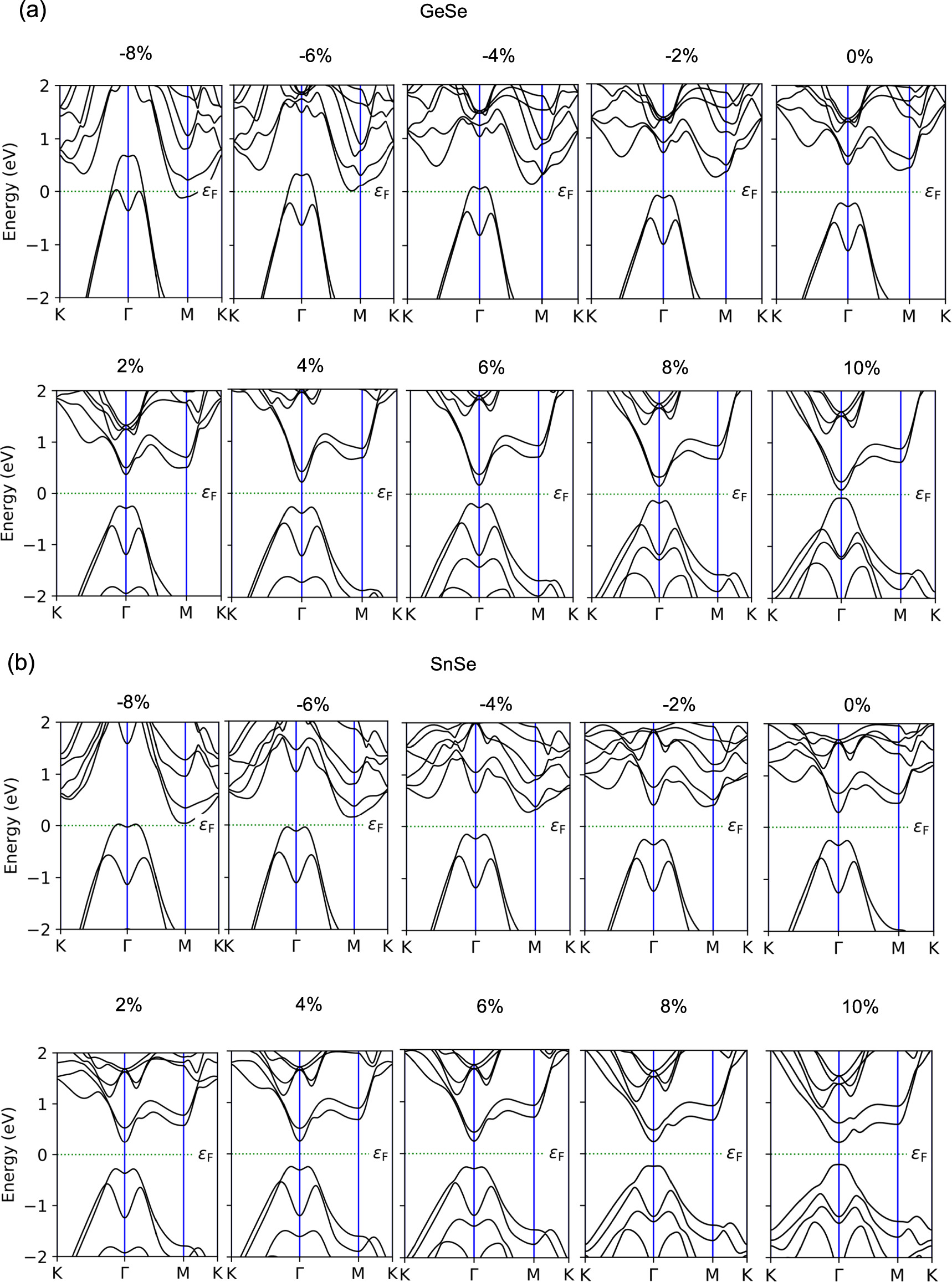
Figure 2. Band structure of bilayer γ-GeSe and γ-SnSe under -8 % to 10 % of strain.
Download figure:
Standard image High-resolution image
Figure 3. (a) Band gap as a function of applied strain for bilayer γ-GeSe and γ-SnSe. (b) Projected band structure for bilayer γ-GeSe and γ-SnSe under -4/-8 % and 10 % strain. (c) Partial charge density corresponding to the valance band maximum (VBM) and conduction band minimum (CBM) for bilayer γ-GeSe and γ-SnSe under -4/-8 % and 10 % strain. (d) Bond length and thickness as a function of applied strain for bilayer γ-GeSe and γ-SnSe.
Download figure:
Standard image High-resolution imageApplying an external electric field perpendicular to layered materials is another effective method for tuning the physical properties of 2D layered materials. We next examine the response of the energy band gap of the bilayer γ-GeSe and γ-SnSe to an external electric field. The evolution of the band structure with varying electric field strength is depicted in figure 4. It is observed that the band gap decreases monotonically as the electric field strength increases, eventually closing at 5 V/nm for bilayer γ-GeSe and 7 V/nm for bilayer γ-SnSe. This variation of the band gap as a function of the applied electric field for bilayer γ-GeSe and γ-SnSe is also presented in figure 5(a). To gain deeper insights into the electronic structure engineering by electric field, we plot the projected band structure and partial charge density of the valence band maximum (VBM) and conduction band minimum (CBM) for bilayer γ-GeSe and γ-SnSe under 0 V/nm and 5/7 V/nm electric fields in figures 5(b) and (c). As shown in the figures, the overall shape of the energy bands for the bottom and top layers remains very similar, regardless of the presence of a 5/7 V/nm electric field. However, the energy bands of the bottom layer shift upwards, while those of the top layer shift downwards, gradually reducing the band gap. This band gap engineering by an external electric field can be explained by the charge redistribution in bilayer γ-GeSe and γ-SnSe under an electric field, as illustrated in figure 5(d). The charge density difference (Δρ) is defined as Δρ = ρE − ρ0, where ρE and ρ0 are the charge densities of the bilayer γ-GeSe and γ-SnSe with and without the external electric field, respectively. Positive (negative) Δρ indicates charge accumulation (depletion). As observed in the figure, there is charge accumulation in the bottom layer and depletion in the top layer. This leads to the VBM in the bottom layer shifting upwards and the CBM in the top layer shifting downwards, which consequently reduces the energy band gap. This modulation of the band gap, resulting from charge redistribution to the top and bottom layers by the electric field, is referred to as the giant Stark effect, as previously proposed in the case of phosphorene nano ribbons [41].

Figure 4. Band structure of bilayer γ-GeSe and γ-SnSe under 0 V/nm to 7 V/nm electric field.
Download figure:
Standard image High-resolution image
Figure 5. (a) Band gap as a function of applied electric field for bilayer γ-GeSe and γ-SnSe. (b) Projected band structure for bilayer γ-GeSe and γ-SnSe under 0 V/nm and 5/7 V/nm electric field. (c) Partial charge density corresponding to the valance band maximum (VBM) and conduction band minimum (CBM) for bilayer γ-GeSe and γ-SnSe under 0 V/nm and 5/7 V/nm electric field. (d) Charge redistribution for bilayer γ-GeSe and γ-SnSe under 5/7 V/nm electric field. The blue (red) isosurfaces represent charge accumulation (depletion).
Download figure:
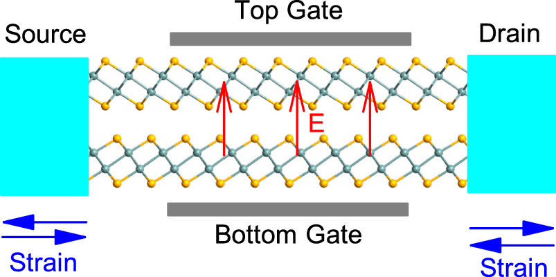
Standard image High-resolution imageBased on the aforementioned strain and electric field modulation of the band gap of γ-GeSe and γ-SnSe bilayer, we have designed a nanoscale transistor. This transistor comprises a bilayer of γ-GeSe or γ-SnSe situated in the middle, with the source and drain located on the left and right sides, respectively. These sides are capable of applying strain, while the top and bottom gates, positioned above and below the bilayer, can apply an electric field (figure 6). When compressive strain is applied, the band gap is reduced. Once the strain reaches a critical point, the band gap closes, and the transistor enters the ON state. As the strain is reduced, the transistor reverts to the OFF state. Similarly, gate voltage can be used to control the electric field applied to the bilayer. When the electric field reaches its critical point, the band gap also reduces to zero, turning the transistor ON. As the gate voltage decreases, the transistor switches back to the OFF state. Therefore, by utilizing both strain and electric field, the creation of a nanoscale transistor based on γ-GeSe and γ-SnSe bilayer can be achieved.
Figure 6. Schematic diagram of a strain and electric field controlled nano scale transistor based on bilayer γ-GeSe and γ-SnSe.
Download figure:
Standard image High-resolution image
4. Conclusion
In summary, both strain and external electric fields can effectively engineer the band gap of bilayer γ-GeSe and γ-SnSe. The band gaps of bilayer γ-GeSe and γ-SnSe are sensitive to both compressive and tensile strains. Tensile strain can even lead to a transition from an indirect to a direct band gap. This band structure engineering through strain results from changes in the Ge/Sn-Se bond length induced by the strain. Additionally, the band gaps of bilayer γ-GeSe and γ-SnSe can also be engineered by electric fields, which may even result in a semiconductor-to-metal transition. The underlying mechanism for this band gap tuning is the charge redistribution caused by the electric field. Our findings suggest that band gap engineering through strain and electric fields is a promising approach for the development of next-generation nanoelectronic and optoelectronic devices based on bilayer γ-GeSe and γ-SnSe.
Acknowledgments
This work is supported by Singapore A*STAR IRG (A2083c0057). All the calculations were carried out using the computational resources provided by the National Supercomputing Centre (NSCC) Singapore.
Data availability statement
All data that support the findings of this study are included within the article (and any supplementary files).