

Abstract
Nanoscale conductive materials are often used for inducing localized free electron oscillations known as plasmons. This is due to their high electronic excitability under optical irradiation owing to their super-small volume. Recently, plasmons have been of interest for enhancing the gain-bandwidth product of optical amplifiers. There are currently two well-established mechanisms for light amplification. The first one is via stimulated emission of radiation (lasers) using a given energy source and often an optical feedback mechanism. The second one is based on the nonlinear coupling of a low-intensity input wave and a high-intensity pump wave for energy exchange (parametric amplifiers). Both techniques have shortcomings. Lasers have a small operation bandwidth and offer a limited gain, but require moderate energy pumping to operate. Whereas optical parametric amplifiers (OPAs) offer a high operation bandwidth along with a much higher optical gain, with the drawback of requiring intense pumping to be functional. The aim of this paper is to introduce a technique that combines the advantages and eliminates the drawbacks of both techniques in the nanoscale to allow for a better amplification performance in integrated optical devices. This is achieved by inducing a plasmonic chirp in conductive nanomaterials a.k.a nano-antennas, which enables the confinement of an enormous electric energy density that can be coupled to an input beam for amplification. Using the Finite Difference Time Domain numerical-method with the material parameters of well-known semiconductors, intramaterial condensation of electric energy density is observed in semiconductor nano-antennas for certain plasmonic chirp-frequencies which enables broadband high-gain optical amplification based on free-electron oscillations that is promising for small-scale optical devices requiring a high gain-bandwidth product. The results are in good agreement with semiempirical data.
Export citation and abstract BibTeX RIS

Original content from this work may be used under the terms of the Creative Commons Attribution 4.0 license. Any further distribution of this work must maintain attribution to the author(s) and the title of the work, journal citation and DOI.
1. Introduction
Plasma oscillations occur in conductive media where free electrons are generated under electromagnetic irradiation [1], a quantum of which is referred as plasmons [1, 2]. In the last decade there has been an interest on the use of plasmons for enhancing both the gain-factor and the gain-bandwidth of optical amplifiers [3–6]. Currently, most optical amplifiers are based on the technique of stimulated emission of radiation, which requires a gain medium, a source to energize the gain medium, and often a stable optical feedback mechanism [7, 8]. These optical amplifiers are very commonly referred as lasers. It is well-known that lasers are quite limited in their gain-bandwidth product. This is because their performance depends on the intrinsic properties of the employed gain medium, which usually offers a limited gain over a narrow spectral band. As a result, in many applications, the limited gain-bandwidth product constrains the performance and capabilities of the overall optical system as lasers are usually the most fundamental component in an integrated optical system. This limitation of stimulated emission based amplifiers can be avoided by using optical parametric amplifiers (OPAs) which can simultaneously provide a very high optical gain, and a large user-controlled bandwidth, thereby allowing for a huge gain-bandwidth product [8–11]. For this reason, at first sight OPAs may seem to be the ultimate solution to enhance the amplification capabilities of integrated optical devices. However, OPAs require very high pump intensities to provide a gain factor that can surpass that of lasers. Furthermore, this requires large and bulky energy sources and hinders the feasibility of employing OPAs in integrated photonic devices [7, 8].
Different designs and scenarios have been proposed to come up with the ideal optical amplifier configuration, especially for the case of OPAs [7–11]. A prominent technique is the creation of artificial materials with extraordinary electrical non-linearity to provide OPA at a lower pump wave intensity. Other techniques involve altering the structure of an OPA system for super-nonlinearity, or to excite the structure in a special manner such that an extraordinary non-linearity is induced [8]. This indeed relaxes the high-intensity requirement for a given pump wave during OPA, but it still does not make OPAs favorable in small-scale optical devices due to the requirement of a sufficient interaction medium length, which should be on the order of centimeters [10]. On the other hand, lasers can be employed in small-scale devices while enabling sufficient optical gain for many applications, albeit within a narrow bandwidth. For lasers, the issue of having a low gain-bandwidth product is usually only solvable from the gain point of view via increased optical pumping (up to the saturation power). The operation bandwidth of lasers remains fixed in most practical designs, although limited tunability can be achieved for some cases. Currently, research on OPAs mostly continues because of their potential to replace lasers, in case the requirements of applying a high-intensity pump, and using a bulk/centimeter-scale interaction medium are partially resolved using certain implementations and operation conditions.
In the last decade, optical amplification based on plasma oscillations (plasmons) has been investigated for a possible combination of the advantages of lasers and OPAs [12–14]. Based on these investigations, it can be inferred that plasmons can be utilized to attain optical amplification with a high gain-bandwidth product. However, optical amplification via plasmons, usually, also requires intense optical pumping (although relatively less than OPAs), especially for higher frequencies. Moreover, the gain is quite limited in the small-scale just as in the case of OPAs. Therefore, the problem of attaining optical amplification with a high gain-bandwidth product in the small-scale under moderate optical pumping, remains a big challenge. The main issue is to stimulate plasmons that are strong enough to induce and confine the required electric energy density that can be used for the amplification of an input beam with a gain-bandwidth product that can surpass that of lasers and OPAs.
Consequently, the aim of this study is to propose a solution to this problem by suggesting a simple small-scale optical system that can eliminate the aforementioned drawbacks to be eligible for being used as an efficient amplifier in small-scale integrated photonic devices. Here, semiconductor nano-antennas are investigated for their suitability as high-efficiency plasmonic optical amplifiers. There are two reasons for the preference of semiconductor nano-antennas: The first one is the small volume of nano-antennas, as inducing strong plasma oscillations is easier in small volumes [15–17]. The second reason is that dielectric structures are impractical for generating free electrons. Importantly, semiconductors are more favorable for plasmonic optical amplification compared to metals, as metals have strong absorption characteristics that would greatly reduce the rate of amplification of an incoming optical beam. Therefore, in this study, we will focus on generating plasmonic chirps in semiconductor nano-antennas via free electron density modulation, which may yield strong optical amplification through electromagnetic energy accumulation under the undulation of the effective permittivity due to the corresponding fluctuation in bound charge polarization. A plasmonic chirp can be induced by intensity-modulated optical pumping as shown in figure 1. Hence, this paper examines the interaction of an incoming low-intensity electric field with a semiconductor nano-antenna throughout an intensity modulated optical pump. The goal is to show that a high optical gain can be attained this way over a huge bandwidth, even under moderate optical pumping. This is to be achieved by the confinement of a huge electric energy density within the nano-antenna through a continuously modulated refractive index via an intensity-modulated optical pump, which induces a plasmonic chirp that eases the transmission of an input wave (to be amplified) into the material, but hinders its retransmission into the air, thereby trapping it under strong fluctuations in bound charge polarization. While the input beam is trapped within the nano-antenna, the energy is transferred from the optical pump to the medium, which then transfers it to the input beam. Next, we discuss the underlying mechanism.
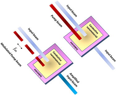
Figure 1. Amplification of an input beam under modulated optical pumping.
Download figure:
Standard image High-resolution image2. Methods
To analyze light amplification via plasmonic chirps, which can be produced by carrier injection rate modulation using an intensity-modulated optical pump in semiconductor nano-antennas, the semi-classical modeling approach is followed. The input beam to be amplified is treated as a wave and modeled using the wave equation, whereas the electron dynamics are modeled using the rate equation. These equations are coupled through the Lorentz dispersion equation to model the charge polarization dynamics. For simplicity, a gain medium with a single electronic transition is considered, which is quite realistic in many cases (such as Nd:YAG, ruby, and Titanium Sapphire). The concurrent solution of these equations enables one to observe the amplitude variation of the input wave in time. Since we are only interested in the amplitude of the input wave while it is undergoing amplification, beam characteristics such as cross-sectional shape and spot-size are ignored. Hence, a one dimensional spatial modeling is carried out. As some of the induced plasmonic chirps are expected to yield a very high intensity for the amplified input wave, for an accurate modeling of the dispersion characteristics of the underlying semiconductor nanomaterial, one should use the nonlinear form of the Lorentz dispersion equation for modeling the carrier dynamics. The coupling of the wave equation and the nonlinear Lorentz dispersion equation occurs through the polarization density term 
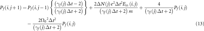
The modulated high-intensity optical pump that energizes the semiconductor nanomaterial via the formation of a plasmonic chirp, is included as the intensity term (within the carrier injection term) in the rate equation, which is a sinusoidal function of time whose frequency (plasmonic-chirp or modulation frequency  ) needs to be adjusted/set for the maximization of the monochromatic input wave amplitude at a selected input wave frequency. Hence, we ultimately have an optimization problem, in which it is assumed that the pump intensity envelope has a sinusoidal variation associated with an intensity modulation frequency
  that is swept over a range of modulation frequencies in order to search for the maximum input wave electric field amplitude. It might be the case that there are many modulation/plasmonic-chirp frequencies that yield a high input wave electric field intensity. Consequently, there can be many carrier-injection functions
  that yield the desired input wave electric field intensity level (gain factor) at a given input wave frequency.
Hence, our investigation involves the concurrent solution of the wave equation, Lorentz dispersion equation, and the associated rate equation that model the carrier dynamics. These equations are expressed as follows [18–21]
Wave equation:

Nonlinear Lorentz dispersion equation for bound electrons:

Lorentz dispersion equation for free electrons:

Rate equation:


Evidently, the wave dynamics and the electron dynamics are coupled through the polarization density, which depends on the transition carrier density (density of population difference between the conduction and the valence band) whose dynamics are determined by the pumping rate and the lifetime of the carriers at each state.
Figure 2 illustrates the associated electron dynamics that are described via equations (4)–(7). Optical pumping raises electrons from the ground level to an excited vibrational state, from where the electrons quickly fall to the upper electronic state that is the bottom of the conduction band. The electrons then recombine to the top of the valence band through several mechanisms, which involve radiative and nonradiative recombinations. Under moderate carrier densities, radiative recombination is more prominent, through which a given electron that recombines spontaneously releases a photon. The radiative recombination rate depends linearly on the carrier density at the upper electronic state. When the carrier density at the upper electronic state is either very low or very high, nonradiative recombination is more prominent. At low carrier densities, the nonradiative recombination mainly occurs due to the presence of defect centers, impurities, and traps within the semiconductor material [21]. Conversely, if the carrier density is high, nonradiative recombination mainly occurs due to Auger recombination, which is proportional to the square of the carrier density [21].

Figure 2. Electron dynamics, which involve excitation from the ground state, recombination mechanisms, and fast thermal decay, with the corresponding electron populations  at each level, where
  .
.
Download figure:
Standard image High-resolution imageUpon investigating equations (1)–(7), one can see that additional nonlinearity is introduced into the system due to the presence of the radiative recombination term  , and the Auger recombination term (
 ). Since the density of carriers undergoing transition is usually quite high within semiconductor nanomaterials (even under moderate pump intensities) [22–24] due their extremely small volume, Auger recombination often dominates the recombination process and has to be taken into account.
Equations (1)–(7) are solved under input and pump excitations. The optical pump is modeled as the time-varying intensity term in equation (6), which has a sinusoidal variation with a frequency of  . Its peak intensity
  can be expressed in terms of the pulse energy of the pump-laser
  , the pulse duration of the pump
  , and the cross-sectional area of the pump-beam


In our analysis, the input wave electric field is numerically excited as a soft-source at a particular point in one-dimensional space, which is designated as the excitation axis (see figure 3)


Figure 3. Configuration for the FDTD analysis of the aforementioned problem.
Download figure:
Standard image High-resolution imageConcerning memory restrictions in an open-boundary computational investigation, the outgoing waves are attenuated using perfectly matched layers (PMLs), which are implemented based on the given formulation in [19]. After inserting equations (8)–(10) into equations (1)–(7), the amplitude variation of the input wave  can be attained at a given point in one-dimensional space, and the gain-factor of the amplification can be found for a given input wave frequency
  , intensity modulation frequency
  , and pump frequency
  . The resulting plasma oscillation that forms within the semiconductor nano-antenna is described by the periodic variation in transition carrier density
  which causes a chirp in the plasmon frequency
  with a chirp frequency
  . The values of the plasma oscillation parameters {
 ,
,  } depend on the intensity of the pump [25–28]. Throughout the simulations, the nano-antenna length is set to 300 nm.
To solve for the amplitude variation of the input wave electric field at each time-step, equations (1)–(4) are discretized and solved using the Finite difference time domain (FDTD) discretization [18, 19] as follows

Hence, the complete set of discretized equations for solving the aforementioned problem involves equations (11)–(14). Here the spatial and temporal sampling must be done carefully as the FDTD method can lead to significant discretization error for nonlinear problems even under the satisfaction of the Courant's stability condition. The discretization error can be minimized by choosing the temporal and spatial discretization,  and
and  , as small as the available computational sources such as memory and processing power allow. This leads to an exponential increase in the cost of computation, but since the problem is nonlinear and prone to error propagation, fine-discretization is usually worth the increased computational cost.
3. Practical implementation
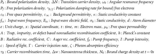
The practical set-up for light amplification via free electron density modulation in a semiconductor nano-antenna is shown in figure 4. The monochromatic pump light (with frequency  ) is initially passed through a strongly nonlinear crystal (such as Lithium-Niobate) along with the monochromatic modulating light (with frequency
  ), after which the second order harmonics (
 ,
,  ), and the sum/difference frequencies (
 ) will be generated. The sum/difference frequency components are transmitted by an optical bandpass filter with the magnitude response indicated in figure 4, and the second order harmonics are filtered out. The output of the optical filter is combined with the input light through the use of a mirror and a beam-splitter. The superposition of the input and the modulated pump beam is sharply focused by a lens onto the semiconductor, which is mounted on a substrate. Both beams propagate through the semiconductor, within which the intensity-modulated optical pump effectively modulates the carrier density, and hence the corresponding effective permittivity, which causes them to be trapped inside the nano-antenna. This way, energy can be accumulated within the semiconductor nano-antenna for long durations, and some of this energy can be transferred to the input beam via free electron oscillations at the same (input beam) frequency, resulting in its amplification. Upon examining equations (4)–(6), one can see that since the nano-antenna thickness is very low, the carrier injection rate is quite high, even at moderate pump intensities.

Figure 4. Practical setup for the implementation of light amplification by free electron density modulation (plasmonic chirp) via intensity-modulated optical pumping through a semiconductor nano-antenna.
Download figure:
Standard image High-resolution image4. Results
4.1. Use of Gallium-arsenide as a semiconductor nano-antenna for plasmonic-chirp induction
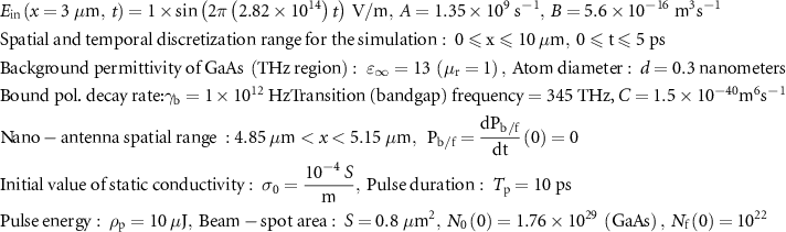
The computations are performed for Gallium arsenide using equations (1)–(7), assuming an Nd:YAG laser-based input wave with a frequency of 282 THz, pulse duration of 10 ps, and an amplitude of 1 Volt/meter. The optical pump originates from a 10 µJoule-laser with a pulse duration of 10 ps and a frequency of 400 THz. The semiconductor nano-antenna (GaAs) has a longitudinal thickness of 300 nm and a cross-sectional area of 0.8  . The wave and medium parameters for the simulation are set as follows [18–21]
The pump intensity is modulated with a modulation frequency  (plasmonic chirp rate) that is swept from 1 THz to 250 THz with 1 THz increments. Hence, the pump intensity is expressed as
Using the discretized equations (equations (11)–(14)), the corresponding peak-amplitude of the input wave is computed for various pump-intensity modulation frequencies. The input wave amplitude  is maximized for certain pump-intensity modulation frequencies, which correspond to the maximization of the electric energy density
  within the semiconductor nano-antenna. For other pump-intensity modulation frequencies, both the input wave amplitude and the energy density remain relatively insignificant. These modulation frequencies correspond to the formation of a suitable time-grating that allows for an efficient energy build-up via letting each incoming pump pulse in during impingement, but not letting them out during the contact for re-transmission into the air (see figure 5).
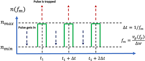
Figure 5. Temporal refractive index variation for trapping pump pulses ( ).
).
Download figure:
Standard image High-resolution imageSince the accumulated energy in the nano-antenna can only be efficiently transferred to an input wave of certain frequency under strong polarization [29–33], the simultaneous maximization of the polarization density in the nano-antenna is equally important. The strong amplification of an input wave is associated with the transfer of the accumulated energy in the medium via free and bound electron polarizations. The polarization of bound electrons enables the confinement or storage of the energies of trapped pump pulses, while the free electrons transfer this stored energy to the input wave during their oscillation at the input wave frequency. Upon examining figures 6(a), (b) and (d), one can deduce that it is due to the simultaneous enhancement of the electric energy density and the polarization density at certain pump-intensity modulation frequencies that the input wave is strongly amplified [34–37].
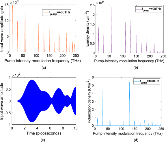
Figure 6. Input wave amplitude gain (a) and energy density (b) variations versus pump-intensity modulation frequency. Temporal variation of the input wave amplitude at 282 THz for a pump-intensity modulation frequency of  (c). Polarization density versus pump-intensity modulation frequency (d). The gain peaks for the input wave coincide with the peaks of the electric energy and polarization densities.
Download figure:
Standard image High-resolution imageFigures 6(a) and (b) show the maximum input wave amplitude that has been attained in the semiconductor nano-antenna and the corresponding electric energy density in the medium, against the pump-intensity modulation frequency, up to a modulation frequency of 250 THz. For certain modulation frequencies ( , the input wave amplitude, electric energy density, and the polarization density are concurrently maximized in agreement with the theoretical prediction. As an arbitrary example for this case, the corresponding temporal variation of the input wave amplitude for
  is illustrated in figure 6(c). Here the input wave is amplified at
  within a duration of 3 ps, beyond which its amplitude fluctuates in line with the polarization dynamics, which depend on the pump-intensity modulation.
The intensity modulation of the optical pump causes a modulation in the free electron density (see figure 7(a)) at the given frequency, with a minimum value of  and a maximum value of
  . Correspondingly, the bound electron density (see figure 7(b)) oscillates between
  and
and  at the given modulation frequency. These modulations of the free electron (carrier) and bound electron densities lead to the modulation of the effective permittivity according to the following relation [18–21]
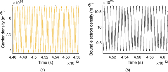
Figure 7. Time variation of the transition carrier density (a) and bound electron density (b).
Download figure:
Standard image High-resolution imagewhich is analytically derived from the linear Lorentz dispersion equations for free and bound electrons and can be used to assess the variation of the refractive index w.r.t the variations in the free and bound electron densities.
Table 1 shows the resulting gain-spectrum of the input wave for the pump intensity-modulation frequency of 109 THz. Since the confined energy density is very large for this modulation frequency, strong input wave amplification can be realized over the entire infrared-ultraviolet spectral range. This is a case of super-broad band optical amplification, unlike stimulated emission which only allows for narrowband amplification.
Table 1. Input wave gain-spectrum, and the confined energy density in the nano-antenna for  .
.

|

|

|
|---|---|---|
| 200 |

|

|
| 400 |

|

|
| 600 |

|

|
| 800 |

|

|
| 1000 |

|

|
4.2. Use of a silicon nano-antenna for plasmonic-chirp induction
The computations are repeated for a silicon nano-antenna with a transition frequency of 272 THz, for an input wave (Indium-Phosphide laser) with a frequency of 194 THz, pulse duration of 10picoseconds, and a normalized amplitude of 1 V m−1 . To observe the effects of decreased pump intensity, this time the pump wave is assumed to be generated by a 5 µJ-laser with a frequency of 400 THz (also 10 picoseconds in duration). The silicon nano-antenna has a longitudinal thickness of 300 nanometers and a cross-sectional area of 1  . In this case, the wave and material parameters are given as follows
Noticeably, due to the reduction in the pump intensity, there appears to be strong input wave amplification around fewer pump-intensity modulation frequencies 
 which are illustrated in figure 8(a). As before, these are the pump-intensity modulation frequencies for which the energy and the polarization densities are concurrently maximized (see figures 8(b) and (c)). This observation reinforces our inference that the pump-intensity modulation frequencies which lead to strong input wave amplification, are the modulation frequencies where the energy transfer is much stronger as a result of enhanced polarization density (see figure 8(d)). It is important to note that, practically, a precise modulation of the pump-intensity at a particular modulation frequency can be challenging due to equipment limitations. Hence, it is better to attain many pump-intensity modulation frequencies that yield a strong input wave amplification (which requires a stronger pump), so that one can choose the most feasible one among them. The resulting temporal variation of the input wave is given in figure 8(c) for
  . The input wave is amplified within 3.5 picoseconds, after which it reaches a polarization saturation and fluctuates in amplitude based on the dynamics of equations (1)–(4).
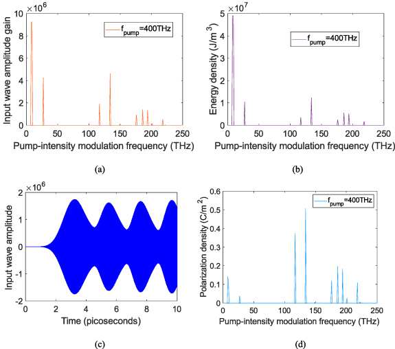
Figure 8. Input wave amplitude gain (a) and energy density (b) variations versus pump-intensity modulation frequency. Temporal variation of the input wave amplitude at 194 THz for a pump-intensity modulation frequency of  (c). Polarization density versus pump-intensity modulation frequency (d). The gain peaks for the input wave coincide with the peaks of the electric energy and polarization densities.
Download figure:
Standard image High-resolution imageThe associated modulations in the free and bound electron densities that induce the plasmonic chirp, are given in figures 9(a) and (b). Notice that the peak value of the carrier density is greater than the peak value of the bound electron density, implying a phase transition from semiconductor to metal, which is taken into account in equations (1)–(4) via the polarization decay and conductivity terms.
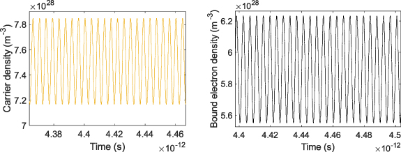
Figure 9. Time variation of the transition carrier density (a) and bound electron density (b) for the case in 3.2.
Download figure:
Standard image High-resolution imageTable 2 shows the gain-spectrum of the input wave for the pump intensity-modulation frequency of 117 THz. Strong input wave amplification is observed once again over the entire infrared-ultraviolet spectral range owing to the large electric energy density induced in the nano-antenna.
Table 2. Input wave gain-spectrum, and the confined energy density in the nano-antenna for  .
.

|

|

|
|---|---|---|
| 200 |

|

|
| 400 |

|

|
| 600 |

|

|
| 800 |

|

|
| 1000 |

|

|
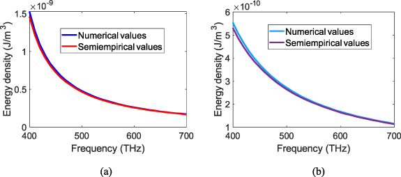
5. Semiempirical versus numerical stored-electric-energy computations
The attained numerical results are compared with semiempirical ones in terms of stored-electric-energy density. Under a pump intensity of  that induces a transition electron density of
  in Silicon and GaAs within the spectral range
  which is far beyond the resonance frequencies of both materials, a reliable comparison can be made due to the convergent behavior of the electric energy density in association with the deviation from the resonance frequency [38–41]. The semiempirical expression for the induced electric energy density by the input wave
  is given as [19–21]

Since the computational results are obtained by solving the Lorentz dispersion equations along with the wave equation (equations (1)–(4)), the computationally attained electric energy density is expressed in terms of the polarization density P [18–21]

The resulting comparison of the numerical and semiempirical results is given in figure 10 within the visible range (400 THz–700 THz). The results mostly agree over the whole bandwidth. The considerable difference between the results for the interval 400 THz–500 THz is due to the effect of increased nonlinearity within this band, which is included in the numerical formulation, but not accounted by the semiempirical formula. The difference between the numerical and semiempirical results converges to zero because of diminished nonlinearity as one gets away from the resonance/transition frequency.
Figure 10. Comparison of the numerical and semiempirical results under the given parameters for GaAs (a) and silicon (b).
Download figure:
Standard image High-resolution image
Regarding experimental feasibility, here the material parameters are chosen to be the actual values of Gallium arsenide, and the frequency of the laser beam is that of an Nd:YAG laser. The pump energy and the pump duration are chosen to be the typical values of ultrashort pulses produced by mode-locked lasers in practice. Therefore the analysis discussed here is directly applicable to experiment. Regarding the attainability of such high pump powers in practice, since the pump duration is ultrashort and the nanoantenna cross-section is very small, under precise focusing towards the nanoantenna surface by an optical lens, such input power is quite practical and realistic given that the light-matter interaction occurs through ultrashort pulses and nano-sized materials. The high-intensity induced optical damage for GaAs is known to occur for intensities above  which is above the intensity levels that are discussed in section 3.
6. Conclusion
Plasmonic-chirp based light amplification in semiconductor nano-antennas is a cost effective amplification technique in terms of pump power and the gain per unit-length. Under similar optical pump power-levels, plasmonic-chirp based light amplification in semiconductor nano-antennas yield a much higher gain per unit-length compared to parametric amplifiers, which is greater by a factor of  assuming an identical longitudinal interaction length. Whereas compared to stimulated emission based amplifiers, the gain per-unit length is greater by a factor of
  . On the other hand, the required pump-power level for amplification is the same with parametric amplifiers, but greater by a factor of
  compared to stimulated emission based amplifiers for attaining the same gain per-unit length. Broadband high-gain light amplification is practically feasible using semiconductor nano-antennas under intensity-modulated optical pumping, given that the resulting plasmonic chirp occurs at a frequency that concurrently maximizes the electric energy density and the polarization density. Over a given spectral range of analysis, many pump-intensity modulation frequencies can be observed to induce such concurrent energy and polarization maximization via associated refractive index modulations that effectively confine high energy densities. The number of these energy-confining modulation frequencies can be increased over a given spectral range via increasing the intensity of the pump pulses. When one of these optimal pump-intensity modulation frequencies is selected for plasmonic-chirp induction in the nano-antenna, high-gain amplification of the input wave can be realized over the entire infrared-ultraviolet range. Hence, the proposed method combines the advantages of lasers and optical parametric amplifiers and yields a high gain-bandwidth product in nano-sized interaction media.
Data availability statement
All data that support the findings of this study are included within the article (and any supplementary files).
Code availability
Available from the author upon reasonable request.
Conflict of interest
On behalf of all authors, the corresponding author states that there is no conflict of interest.
Funding statement
This research received no external funding.