

Abstract
Roll-to-roll (R2R) processing on film substrates has been demonstrated to have the potential for achieving high throughput manufacturing of organic electronic systems at low cost. However, the ever-growing mobile devices market accompanied by the developments in information and communication technologies require high performance systems at very low power operation, sometimes on larger substrates having sizes in the range of a few metres. Organic electronics often fall short of fulfilling the required computing performance and power requirements of most of the common use cases. Hybrid integration of inorganic monocrystalline silicon chips on polymer films is a means to fulfil the aforementioned requirements. In this context, it is opportune to report our recent activities on R2R processing of plastic films for hybrid integration of flexible electronics. Hybrid integration can be performed with conventional, rigid surface mount devices as well as flexible, ultra-thin bare silicon chips. The first section of the paper is dedicated to a brief overview of R2R manufacturing of electronic devices with an example of production of radio frequency identification tags as well as to a discussion emphasising the targets for hybrid integration. Then, detailed descriptions about our processes for R2R manufacturing of metal wiring lines on films and hybrid integration are included. Three-dimensional integration of films and a temperature sensor label manufactured using hybrid integration process are also elaborated on. Furthermore, key results from fatigue reliability assessment of R2R metallised wiring lines are reported. Finally, some of the challenges in transferring the R2R processes for hybrid integration on film substrates from research labs to industrial manufacturing are highlighted.
Export citation and abstract BibTeX RIS

Original content from this work may be used under the terms of the Creative Commons Attribution 3.0 licence. Any further distribution of this work must maintain attribution to the author(s) and the title of the work, journal citation and DOI.
1. Introduction
With the emergence of wearable electronics [1] combined with the burgeoning interest in novel, low cost electronics for niche markets like smart textiles [2, 3], prosthetics [4, 5] and point-of-care diagnostics [6–9] in recent years, flexible electronics have received increasing attention. Flexible electronics is a collective term applied to any kind of electronic system that is conformable and bendable. Such flexible electronic systems are often fabricated using plastic films due to the multitude of valuable properties exhibited by plastic films such as very good flexibility and foldability, high surface quality, lightweight, thin form factor and large area manufacturing feasibility. Implementing roll-to-roll (R2R) processes for handling the plastic films yields several benefits, namely, low cost, fast mass manufacturing, high throughput and hybrid integration possibility to integrate organic as well as inorganic components [10–16]. In principle, R2R processing of plastic films for flexible electronics manufacturing is quite analogous to the processes followed in paper printing industry where desired characters are printed on rolls at speeds of several hundreds of metres per minute at lower cost. However, R2R manufacturing of flexible electronics is still a developing field with several challenges yet to be addressed before transferring the technology to industrial manufacturing environments.
Several methodologies for manufacturing film based flexible electronics have been demonstrated by various academic as well as industrial research groups over the last decade for manufacturing a variety of devices. However, plastic film based flexible electronic manufacturing can be classified mainly into three approaches based on the materials used in the processes: (a) printed organic semiconductors using thiophenes, pentacenes etc [17–19], (b) inorganic thin film semiconductors with amorphous and polycrystalline silicon, indium gallium zinc oxide etc [20–23] and (c) hybrid integration of monocrystalline silicon chip devices [24–26]. Due to the benefits presented by monocrystalline silicon chips in terms of multi-functionality, high performance, mechanical reliability and lower power requirement, hybrid integration has gained increased interest in the past few years [27–29]. For hybrid integration of components, the wiring lines required for the electrical interconnection between the devices can be patterned using a myriad of different materials and methods [30–37]. In this paper, we explain the techniques practised at Fraunhofer EMFT to fabricate wiring lines on plastic films using R2R processes and hybrid integration using these films.
This paper includes some of our recent activities on R2R processed plastic films for hybrid integrated flexible electronics and it is structured as follows. The paper begins with an overview of R2R process for films and an emphasis on primary technological requirements for hybrid integration in section 2. Section 3 describes the diverse R2R processes followed at Fraunhofer EMFT to produce wiring lines, namely (i) screen printing and (ii) microfabrication. Different procedures pursued for hybrid integration of components, namely (i) flip-chip mounting of ultra-thin silicon chips, (ii) integration of commercial, off-the-shelf components and (iii) self-alignment of ultra-thin silicon chips are discussed in section 4. The processes for 3D integration of foils and the interconnection between the foil layers are explained in section 5. Section 6 presents an application example, a temperature sensor label, manufactured using hybrid integration on a R2R processed film substrate. Section 7 comprises the key results from the fatigue reliability studies of R2R micro-fabricated metallic wiring lines. Concluding remarks and our outlook for future work are included in section 8.
2. R2R processing for production of film based electronics
Over the past several decades, printed circuit board (PCB) technology has been the dominant manufacturing methodology for assembly and integration of electronic components and systems. Rigid PCB boards are thermally stable as they withstand solder reflow processes besides offering good dimensional stability. To date, the worldwide electronics manufacturing industry is primarily PCB based and all processing steps have been optimised targeting high throughput, high reliability and low cost. It is worth mentioning here that any new packaging or system integration technology has to compete with this already established production ecosystem.
In this context, it is interesting to notice that there is a prominent example of an electronic product that has been manufactured on film substrates (instead of well-established PCB) since the very beginning—radio frequency identification (RFID) tags. For more than 20 years, RFID labels are being prepared by R2R processing in their billions and they probably represent one of the cheapest microelectronic product on the market. In addition, the number of RFID tags sold per year has increased gradually with a steady decrease in the selling price: from 100 million tags sold in 2004 at a cost of 1 €/tag to 10 billion RFID tags sold in 2016 at 0.05 €/tag [38]. Therefore, it is worthwhile to have a closer look at this product in order to understand the chances and limits of R2R manufacturing in electronic industry. RFID labels for HF frequencies (13.56 MHz) require a coil antenna that is much larger in size than the integrated circuit (IC) chip and hence it is required to be preferably prepared on a cheap substrate. Besides, there is just one other component to be assembled and interconnected to the antenna which is the IC chip that provides all necessary electronic functions. The IC itself requires only two electrical interconnects which also means that there is no need either for a high precision chip bonding process or for high resolution metal wires on the substrate. Finally, the chip and the antenna must have a very low package height in order to enable integration into the body of a standard chip card that is roughly 0.7 mm thick. All these technical requirements can be satisfied when a plastic film like polyethylene terephthalate (PET) film is used as the substrate material and anisotropic conductive adhesives (ACA) for electrical interconnection at relatively low chip bonding temperatures (below 150 °C). It is fair to conclude that introduction of film substrates and the related development of R2R manufacture have been the dominant reasons for the economic success besides the manifold use cases of RFID labels universally.
An obvious question at this moment is: 'Which technology elements are missing to use high throughput R2R manufacturing for new electronic applications?' Two strong demands posed by current microelectronic industry can be highlighted: (i) thinner chip packages for mobile applications, for instance smartphones and (ii) new applications for flexible electronics, such as wearables and sensors on curved surfaces (including human skin). Film substrates as base material for chip and system packaging actually represent perfect candidates for these future applications and the cost effectiveness of R2R manufacture has already been evidenced as exemplified by the example of RFID labels described earlier. Higher value electronic systems than RFIDs, which can enable new applications within the internet of things (IoT), require at least a sensor, a microcontroller, a power management and a connectivity module. Hence, the hybrid integration of classical microelectronic components with high throughput R2R printing technologies is the key challenge. Classical microelectronic components and especially microcontrollers can have many I/O contacts, usually in fine pitch compared to R2R processing technology capabilities and are therefore not compatible for integration. We propose a chip-foil package approach, where the thinned microcontroller is embedded in a fan-out foil package. The fan-out package is produced in fine pitch and translates the microelectronic connections to R2R compatible relaxed large pitch dimensions. Using such a package, many classical and new applications could be transferred to R2R manufacturing technologies. Therefore, it is persuasive to conclude that film based chip packages for ICs with many I/O contacts with relaxed pitch dimensions represent the key component for many new applications of flexible electronic systems. Thus, the plausible answer to the question in the beginning of this paragraph could be: 'Embedding and electrical interconnection of state-of-the-art IC devices in thin and flexible film packages is supposedly the next important step to enable new applications to be produced with high throughput R2R technology'.
R2R processes can be performed on a wide range of flexible substrates such as polymeric films, paper, textiles, metal foils, ultra-thin glass and ceramic materials (uncured green tape). Each of these substrates show their own specific advantages and limitations. Insulating materials may be preferred when through substrate via holes need to be realised. In case of polymeric films, via holes can easily be prepared by laser drilling. Metal foils show best dimensional stability since shrinking or extension of the web is close to zero. This is beneficial for high accuracy placement of components or alignment of photomasks during lithographic patterning. Glass films exhibit highly effective passivation against water or oxygen that might disturb or destroy electronic functions. Paper rolls are well known from R2R printing technologies. However, the use of paper in electronics would require hermetic sealing against water absorption. Nevertheless, the substrate material portfolio offers plenty of variety for R2R manufacture. Some key properties of three widely used polymeric materials used in R2R processing are listed in table 1. The given numbers should be considered as typical values and the actual material properties may vary strongly between different manufacturers as well as individual products. Furthermore, precise cost based comparison of the polymer film materials depends on the surface treatment and variations in specific properties of the films. Thus, only a rough, relative cost comparison of the films is included in table 1.
Table 1. Key properties of common polymeric substrates [39].
| Property | Polyimide (PI) | Polyethylene naphthalate (PEN) | Polyethylene terephthalate (PET) |
|---|---|---|---|
| Tensile strength (MPa) | 280 | 280 | 230 |
| Glass transition temperature (°C) | — | 155 | 110 |
| Dielectric constant, ε | 3.3 | 2.9 | 3.1 |
| Water absorption (%) | 1.3 | 0.3 | 0.4 |
| Cost | 10 × PEN | 10 × PET | 1 |
Extending the chip-on-foil (COF) applications to state-of-the-art IC devices (e.g. microcontrollers) with multiple I/O contacts requires the successful development of some key enabling technologies. Among these, we emphasise the following targets.
- (a)Availability of IC and sensor devices as thin, bare die components: the simple reason for this demand is that chips or components with conventional thicknesses would require very thick plastic substrates (several hundreds of micrometres) and relatively large roll diameters in order to enable safe rewinding of the substrates in a R2R manufacturing environment. On the other hand, using chips with thicknesses below 30 μm would even allow for completely flexible IC packages.
- (b)Low processing temperatures during manufacture: cost effective PEN substrates can withstand temperatures of roughly up to 150 °C (short time up to 180 °C). Besides, low chip bonding and polymer curing temperatures minimise the residual stress in the resulting chip film package. When higher processing temperatures (e.g. soldering of components) are involved, PI film substrates could be used.
- (c)Robustness of chip-on or in film assemblies: reliability testing and analysis is vital before discussing or starting new production facilities for flexible electronic systems.
In line with these objectives, a pilot line manufacturing environment has been setup at Fraunhofer EMFT in Munich, Germany, to further focus on the technological developments of these targets. The technical infrastructure comprises the following R2R processing equipment.
- Sputtering of thin metal films on web substrates (e.g. Cr, Cu).
- Web to web lamination (e.g. for lamination of dry film photoresist).
- Lithographic patterning consisting of a 20 cm × 20 cm ultraviolet (UV) exposure field.
- Electroplating of copper for fabricating wiring lines up to 10 μm thickness.
- Screen printing of metal, resistive and dielectric pastes at temperatures below 180 °C.
- Slid coating on web substrates.
- Chip bonding (high resolution flip-chip bonding, only on single sheets until now).
- Aligned 'sheet-to-roll' attachment allowing for 3D stacking of film modules of different functionalities.
- Laser cutting and drilling of vias or blind holes.
- Electrical testing of final electronic systems.
These processing instruments support the development and test of multifunctional systems-on-film. Typical width of film substrates (mainly PET, PEN, PI) stands at 215 mm. Detailed information about the processes for thin film metallisation, electroplating and screen printing are presented in the ensuing sections. Technological developments on film based flexible electronics are accompanied by various reliability tests. A specific test apparatus for online electrical testing of flexible electronic modules during repeated mechanical bending was constructed and has been adapted as the routine test method.
3. Fabrication of wiring lines using R2R processing
Metallic wiring lines in a film based electronic system act as transmission lines for conveying various signals such as electric power, communication and data signals in and out of the system as well as in between the several components of the flexible electronic system. Here, we present two divergent methodologies based on R2R processing to fabricate these metallic interconnects: (i) screen printing and (ii) microfabrication based technologies on foils. Both these techniques explained in the sections 3.1 and 3.2 are followed at Fraunhofer EMFT to fabricate fine line metal patterns on plastic films that serve as wiring lines for various application scenarios.
3.1. Screen printing
Screen printing is one of the common methods employed for fabricating metallic wiring lines on films. It is widely used for patterning microstructures on films because of its versatility in being able to print on almost all material substrates and in a variety of shapes besides the reasonable manufacturing cost and high throughput [40]. It enables surface patterning of large areas with materials of relatively high thickness (above 1 μm). Structures having a thickness of up to 35 μm and a minimum resolution of 50–100 μm can be realised using screen printing. We employed flatbed screen printing technique to pattern the wiring lines and the process is illustrated in figure 1. The plastic film substrate in the form of roll is unwound on one end of the printer and it is rewound back into rolls for further processing or transportation at the other end of the printer. In between these two ends of the printer, patterning and curing of the printed structures occur. The process begins with the pouring of the paste or ink on the topside of the screen. Then, the dispensed paste is pressed locally onto the underlying substrate through the apertures of the predefined mesh patterns on the screen and swiped by the rubber blade resulting in a film deposition of controlled geometry and thickness. Subsequent drying and curing of the dispensed paste is performed in an integrated UV exposure zone and a belt oven. Finally, the substrate with printed and cured patterns are spooled back into rolls for further processing steps. For our processes, we used a paste containing silver nanoparticles for printing the wiring lines which offers excellent conductivity due to its very low sheet resistance post curing (Rs < 20 mΩ/□) [41].
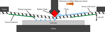
Figure 1. Schematic representations of flatbed single step screen printing process.
Download figure:
Standard image High-resolution imageScreen printing also presents the possibility for multiple layering which has to be performed by following a multistep sequence as described in figure 2. In the first step, a metallic layer with eventual positioning markers for subsequent layers is printed. After curing of the first layer, the second dielectric layer along with positioning markers is printed using a dielectric paste over some areas of the first metallic wiring layer for local insulation. Then, the dielectric layer is cured and a second metallic wiring layer is printed on top of the dielectric layer. Ultimately, a passivation layer is printed to offer complete electrical insulation. By repeating this sequence, several subsequent layers can be printed. One challenge concerning multi-layered screen printing is the precise positioning of various layers over one another. To accomplish this, we implemented image recognition techniques for the positioning markers on each layer to print multi-layered structures. Figure 3(a) presents an array of resistors consisting of two layers, (i) silver wiring lines (white coloured patterns) and (ii) resistor structures (black coloured structures) and figure 3(b) shows an electroluminescent display printed using multi-layered screen printing.
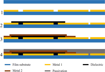
Figure 2. Process flow for screen printing of multi-layered structures.
Download figure:
Standard image High-resolution image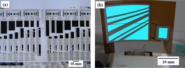
Figure 3. (a) Array of resistors and (b) an electroluminescent display manufactured using multi-layered screen printing.
Download figure:
Standard image High-resolution imageThe selection of materials in screen printing is decisive in the resolution of the printed structures. The choice of the paste along with a screen having a proper mesh type and count compatible to its rheology requires meticulous engineering work and optimisation to attain the desired resolution and thickness. The viscosity of the paste plays a major role in determining the resolution. High viscosity pastes enable the operating personnel to have a better control on the flow speed of the paste onto the substrate than low viscosity pastes. However, high viscosity pastes tend to block the apertures on the screen more often compared to low viscosity pastes and such blocked screen apertures require a series of cleaning steps before the screen can be used again for printing, thus affecting the process speed and yield. Besides, the surface energy of the substrate is equally influential in deciding the speed of paste flow on the substrate. Substrates with low surface energy decelerate the flow of the paste on themselves thereby reducing the wettability of the paste and therefore enhance the resolution of the printed structures. Hence, for printing structures with very good resolution and even edges, a compromise between the viscosity of the paste and the surface energy of the substrate is necessary.
Additionally, the substrate foil must withstand the curing cycles of the printed inks (thermally or UV-cured) with no or reduced shrinkage and warpage. The shrinkage and the warpage of the foil caused during curing can hinder alignment of layers, thereby prohibiting subsequent printing. For an efficient screen printing process, foils withstanding a temperature of at least 150 °C are recommended. Furthermore, very good adhesion of the printed materials to the foil surface is required to prevent peeling or cracking of the printed structures when the substrate is bent. The positioning accuracy is critical in screen printing, especially for printing multiple layers. An accuracy less than or equal to ±25 μm limits the resolution of multi-layered systems. The sharpness of the markers is crucial for printing multi-layered structures since blurred markers affect the image recognition and consequently the positioning accuracy during multi-layered screen printing. However, barring these aforementioned challenges posed by screen printing, the possibility to print multi-layered high definition structures at low cost and high throughput makes screen printing an attractive option for mass production of flexible electronic components.
3.2. Microfabrication technologies for R2R processing
Classical microfabrication approaches that are widely used for semiconductor manufacturing can also be implemented in R2R processing. In this section, we describe the implementation of some of the microfabrication processes such as sputtering, lithography, etching and electroplating to manufacture the wiring lines on plastic film rolls that act as interconnection layers for film based flexible electronics. Here, we present only an overview about the aforementioned process steps and comprehensive information about these processes can be found at [42].
3.2.1. Sputter deposition of thin metal films
Thin metal layers on film substrates can be manufactured using sputter deposition of metallic ions. Prior to depositing the thin metal layer on the film surface, an inline plasma pre-treatment was used for cleaning, activation and modification of the film surface to improve adhesion of the metal. After pre-treatment of the film substrate, a chromium layer having a thickness of few nm was sputter deposited on the film substrate. Then, a 500 nm thin layer of copper was sputter deposited on top of the chromium layer. The chromium layer was used to aid the adhesion of copper to the film substrate since chromium adheres well to most polymers. It has to be noted that a second etching step is necessary to remove the chromium adhesion layer since copper and chromium etching cannot be performed concurrently with the same etchant. Afterwards, the film substrate coated completely with sputtered copper was transferred to the UV photolithographic step to define the desired metallic patterns on the film substrate. A negative tone dry film photoresist (MX5015 manufactured by DuPont™) that can be laminated directly onto the film substrate was employed for the process. The resolution of the fabricated fine metal structures is determined predominantly by the thickness and the stability of the resist as well as its overlying Mylar® coversheet during various processing steps. Hence, scrupulous choice of the resist as well as the overlay is pivotal for manufacturing wiring lines with good resolution and pitch. The lamination of dry film resist on top of the sputtered copper layer was performed using a lamination system from Stork GmbH with the following parameters: temperature—60° to 100 °C; pressure—3 bar; speed of lamination—0.4 to 1 m min−1.
After the lamination of the resist, contact lithography was performed using an OptoLine 2200 system from Ciposa S.A. with a collimated mercury (broadband) light source at an intensity of about 20 mW cm−2. Chromium coated 9'' glass masks used for the exposure permitted the processing of 200 mm wide films. The exposure energy as well as the contact between the mask and the photoresist are the key parameters to be controlled during the exposure. The exposure energy and the developing time determine the resolution of the metallised structures. Two types of contact control namely, (i) proximity contact and (ii) vacuum exposure can be used to control the contact between the mask and the resist. Proper trade-off must be made between the two types of contact to avoid air bubbles while achieving good resolution [42].
The exposed resist was then developed in a R2R developing platform from Höllmüller using 0.5% soda solution (Na2CO3) as the developer at a temperature of 28 °C. Post development, the resist was rinsed with deionised water in a three-stage rinsing cascade. The stability of the resist can be improved to some extent by adding magnesium sulphate (MgSO4) with a concentration of about 350 ppm to the developer in the first rinsing module. After developing the resist, the film roll was transferred to a wet etching bath from Sessler to remove the metallic structures from areas outside the lithographically defined wiring line patterns. The copper seed layer etching step was carried out at a temperature of 28 °C in a chemical bath consisting of 13% sodium persulphate (Na2S2O8) which has an etch rate of about 0–5 μm min−1. An in-built ultrasonic tool was utilised to enhance the exchange of etch medium to the surface of the foil, thereby removing the bubbles that adhere to the tiny resist gaps as the foil was moved in the etch bath. After completion of the copper seed layer etch, the chromium adhesion layer was removed in a separate step in an external bath using a highly diluted alkaline potassium ferricyanide solution (K3Fe(CN)6). Afterwards, the resist was stripped off in an additional bath using a 10% potassium hydroxide solution (KOH) at a temperature of 50 °C. Finally, the plastic film substrate was rinsed with deionized water and dried with hot air flow. The thickness of the metal to be etched away depends on the retention time of the roll in the bath and consequently the speed of the roll during etching. In general, wet etching is a relatively slow process and hence it is decisive in determining the time required for the overall microfabrication process. A polyimide film roll consisting of various copper sputter deposited structures having a thickness of 500 nm and a microscopic view of the sputter deposited wiring lines are depicted in figure 4.

Figure 4. (a) A polyimide roll with 500 nm thin copper sputter deposited structures. (b) Microscopic view of the sputter deposited copper wiring lines.
Download figure:
Standard image High-resolution image3.2.2. Semi-additive metallisation
Thicker layers (∼few μm) of metals for wiring lines can be fabricated using electroplating and the thickness of the electroplated metal layers is defined by the resist thickness. While electroplating is a mature technology for growing thicker metal layers on rigid substrates, alike other microfabrication processes it is rather minimally implemented for processing on flexible substrates such as plastic films. The primary application of electroplating in microfabrication on film substrates is for selective deposition of conductive wiring lines in a resist pattern fabricated by photolithography and resist development. One basic requirement for electroplating is the presence of a seed layer over which the thicker metal films can be grown. Therefore, a thin film metal deposition step such as sputtering or thermal evaporation for depositing the seed layer on films needs to be performed prior to electroplating. Surface contaminants such as polymer residues significantly reduce the adhesion of the dry film photoresist to the copper seed layer and hence a cleaning step is normally recommended to ensure better adhesion of dry film photoresist to the seed metal layer. We removed about 300 nm of copper seed layer prior to electroplating to improve the resist adhesion. We used a continuously operating DC electroplating system for depositing copper layers having a thickness of few μm. The electroplating process was performed using a commercial acid copper bath as the medium in a R2R electroplating equipment from Sessler. The R2R process sequence for fabrication of wiring layers is illustrated in figure 5. Copper lines having a thickness of up to 10 μm can be grown by using electroplating. Figure 6 portrays the microscopic view of 8 μm thick electroplated copper wiring lines. Electrical measurements showed that the specific resistivity of such electroplated copper layer on polyimide film was 1.9 μΩ cm, which is very close to standard copper resistivity of 1.8 μΩ cm [37].
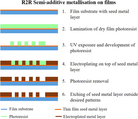
Figure 5. Schematic of microfabrication process of fabrication of thick film metal deposition on films.
Download figure:
Standard image High-resolution image
Figure 6. Microscopic view of 8 μm thick electroplated copper wiring lines on a film substrate. Reproduced with permission from [37].
Download figure:
Standard image High-resolution imageThe semi-additive technology for metallisation offers the possibility to fabricate structures on both sides of the plastic film. As an example, figure 7 shows a polyimide foil metallised on both sides manufactured using electroplating. Figure 8 depicts the cross-section of the same film exhibiting the interconnection between the front and the rear side metallisation that was enabled through laser drilled via holes and figure 9 renders an isometric view of a similar double side metallised via hole. The via holes were drilled by a laser in a R2R setup with a galvanometer scanner. The drilled via hole is not cylindrical but rather funnel shaped with a slope of about 50°. Such a funnel shaped, low aspect ratio via hole facilitates the conformal metallisation of the second layer while performing thin film metallisation with sputter deposition. At the bottom of the via hole, the flat interface of the front side metallisation to the rear side metallisation is visible (figure 9).
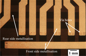
Figure 7. Polyimide film substrate with double side metallisation.
Download figure:
Standard image High-resolution image
Figure 8. Cross-section of the polyimide film substrate showing the interconnection between front and rear side metallisation of the film. Reproduced with permission from [43].
Download figure:
Standard image High-resolution image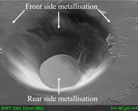
Figure 9. Isometric view of a via hole with the front and the rear side metallisation on a polyimide film substrate.
Download figure:
Standard image High-resolution imageA common problem in the manufacturing of multi-layered flexible electronic systems is the precise alignment of different layers on each other. The problem aggravates when enabling interconnections between the different layers where it is crucial to maintain μm accuracy. In a standard process of drilling via interconnections with a laser, the alignment is performed by reading the fiducial markers that are located at the corners of a sheet. However, due to shrinkage or expansion of the foils resulting from the preceding thermal processes, the real position of an interconnection line may differ from the predetermined location. This deviation may sometimes exceed even 100 μm. One such misalignment of the via holes relative to the metallisation is shown in figure 10(a). This problem can solved by executing a local alignment step. This local alignment can be performed using pattern recognition (to identify the actual position of every single pad) and by calculating the exact location for the laser beam to drill the hole. Figure 10(b) presents perfectly positioned via holes after a local alignment step. Therefore, it can be understood that conscientious processing is necessary for accurate positioning of the via holes relative to the wiring lines, even if the plastic substrate suffered any shrinking due to thermal treatment from earlier process steps.

Figure 10. (a) Misaligned via holes and (b) perfectly positioned via holes.
Download figure:
Standard image High-resolution imageDouble side processed film substrates are especially beneficial for multifunctional system integration that could be the key for manufacturing in the framework of the IoT and Industry 4.0. Furthermore, semi-additive metallised copper has been demonstrated to provide improved performance for high frequency signal transmission (characterised up to 40 GHz) compared to copper wiring schemes prepared by standard PCB technology based on etching of copper clad laminates [43]. Besides, R2R microfabrication processes could also be cost effective for flexible electronics manufacturing since the microfabrication processes can be transferred to industries for mass manufacturing without drastic modifications of the already existing infrastructure.
4. Component assembly on films for hybrid integration
Recent and upcoming flexible electronic systems require energy efficient multifunctional systems with a conformable form factor that are produced cost effectively. As discussed in section 2, hybrid integration of components in R2R processing environment has the potential to emerge as a candidate for mass manufacturing alongside PCB manufacturing. As already sketched, one of the main challenges in hybrid integration is to prepare the conventional components that are traditionally used in PCB technology for integration on thin foils. Fraunhofer EMFT has developed a method to integrate bare silicon dies in films to create chip-in-foil (CIF) packages with fan-out of contacts that are compatible with the relaxed pitch of R2R mass manufacturing. These chip-foil packages and the diverse processes to manufacture them are introduced in section 4.1. Then, a R2R compatible process for integration of these CIF packages and other off-the-shelf components on foils are explained in section 4.2.
4.1. Integration of ultra-thin, bare silicon chip-on films
Ultra-thin silicon chips thinner than 50 μm are one of the most interesting candidates for hybrid integrated flexible electronics due to their potential to deliver high performance while exhibiting mechanical bendability. However, ultra-thin chips are fragile in terms of mechanical handling and they can be broken during assembly. Yet, the handling and processing problems can be addressed when the ultra-thin chips are assembled on flexible film substrates, thus creating COF assemblies and CIF packages [44]. Moreover, enhancement of the mechanical robustness and flexibility of the ultra-thin chips due to embedding in foils has also been proven [45–47]. Such a sturdy chip-foil stacks can be handled and assembled in a similar fashion as a surface mount device (SMD) component at all manufacturing processes used for die assembly. These versatile chip-foil stacks can be created using diverse techniques. In this section, we present two approaches to integrate bare silicon chips on films. Firstly, the more established flip-chip bonding process that is one of the primary die bonding techniques due to its current pervasive usage is explained. Secondly, a novel self-alignment process for the two-dimensional arrangement of silicon chips is described.
4.1.1. Flip-chip bonding
Flip-chip bonding process on flexible film substrates is widely used for integration of display driver ICs, for smartphones or in digital cameras, whose thickness lie in the range of 100–150 μm. However, when implemented to mount bare ultra-thin chips (t < 50 μm), the process is highly challenging owing to the mechanical fragility and flexibility of the chips. Some of the key factors for establishing an effective flip-chip bonding process for mounting bare ultra-thin chips are: (1) quantity of adhesive dispensed for the bonding process, (2) bonding pressure, (3) bonding temperature and (4) the pick-up force exerted by the die pick-up head on the chips. We have established a process protocol after determining the optimal values of these parameters and employed flip-chip bonding process to mount daisy chain chips as thin as 12 μm on PI films. It should be noted that the flip-chip bonding process described here was performed at sheet level on 215 mm wide sheets cut out from the metal patterned rolls. The process sequence of mounting ultra-thin chips on film sheets using flip-chip bonding is outlined in figure 11. At first, foil substrates with cavities and electrical wiring lines were prepared. Then, a commercially available anisotropic conductive adhesive (ACA), Delo AC 245 was dispensed into the cavities and ultra-thin chips were bonded onto the foil substrates using a die bonding equipment (Panasonic FCB 3) to create COF assemblies. An ultra-thin flip-chip bonded COF assembly and the schematic of cross-section of the COF assembly are exhibited in figures 12 and 13 respectively. Optionally, some COF assemblies were further encapsulated with a cover layer to isolate the chips from the external environment thus creating CIF packages as shown in step 4 in figure 11. The thickness of the resulting flexible CIF packages was less than 150 μm. Following the integration process, the yield of the chip bonding process was verified by measuring the daisy chain resistances and it was found to have a good throughput. Four-point probe measurement used to quantify the resistance of a single via interconnect between the chip and the foil revealed a low resistance value of 60 mΩ proving an excellent electrical contact between the chip and the foil [48].

Figure 11. Process sequence of flip-chip integration of ultra-thin chips in foils.
Download figure:
Standard image High-resolution image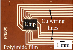
Figure 12. Top view of flip-chip bonded COF assembly.
Download figure:
Standard image High-resolution image
Figure 13. Schematic of cross-section of flip-chip bonded COF assembly.
Download figure:
Standard image High-resolution image4.1.2. Self-alignment of chips
Die bonding and component placement on web substrates are essential prerequisites for manufacturing electronic systems. In case of R2R processing, two requirements must be fulfilled: (i) high alignment accuracy for bonding IC devices with high pin counts and (ii) fast running die handling systems to achieve high throughput. Optical alignment systems are necessary to meet the alignment requirements and its mechanical implementation on conventional tools often results in rather large and expensive die bonding machines. An alternative concept for highly accurate die bonding on large area film substrates is provided by self-assembly and self-alignment techniques.
The working principle is explained in the following lines and is shown in figure 14. Thin silicon chips with a thickness of 50 μm are of lightweight and are able to swim on droplets of fluids like water. If the liquid shows a specific wetting behaviour with respect to the underlying substrate, then the droplet and the chip can move and self-align themselves on the targeted die bonding site. However, such a process requires a surface programming step for the substrate, which defines areas of selective wettability. At first, the polymeric film surfaces are structured with metal patterns, which outline the target areas for die placement. The patterns consist of thin film aluminium or gold and these patterns are prepared preferably in one-step together with the surrounding wiring system. Then, the substrate is placed under a fluorine plasma environment, for instance with CF4 as the active gas component. The fluorine plasma transforms the polymeric film substrate into a strongly hydrophobic state whereas the metal patterns become immensely hydrophilic. Wetting angle for water on the metal pads after fluorine plasma treatment is below 10° while the wetting angle on the polymeric surrounding is above 100° [49]. Next step in the process is to apply a droplet of a polar assembly liquid, for example water, on the metal target area. Then, a thin die is supplied by simply letting it fall down onto the liquid film. Subsequently, the thin and lightweight chip swims on the fluid, which by itself cannot overcome the hydrophobic barrier at the metal pad/polymer interface. The system of chip, fluid and metal pad now turns into a configuration where the surface energy of the liquid is minimised. As the contact areas of liquid/metal and liquid/chip interfaces are constant, the liquid/air interface must be minimised. This minimised state is reached when the chip is orients itself directly above the metal pad. Figure 15 presents different sized chips that are self-aligned on a wafer substrate.

Figure 14. Fundamental process flow of fluidic self-alignment process of thin silicon chips.
Download figure:
Standard image High-resolution image
Figure 15. Self-aligned chips on a wafer.
Download figure:
Standard image High-resolution imageA series of experiments were conducted on a wafer substrate having aluminium target areas and pre-treated with CF4 plasma to determine the self-alignment accuracy of thin silicon chips. The dimensions of the dies and target area were identical. The dies were separated by plasma etching instead of conventional sawing. As the trench pattern for plasma dicing is defined by photolithography, the size of dies was precisely defined with a tolerance of less than 1 μm. Such precision in die dimensions is crucial for the self-alignment accuracy because the surface tension forces and the ideal 'centre position' of the die on the target area are defined by the interface areas. Singulated 50 μm thin test dies that were used for the self-alignment experiments consisted of metal patterns that were visible during infrared (IR) imaging in order to measure any possible shift between the alignment control patterns of substrate and dies. After successful self-alignment of the chips on the wafer substrate, IR microscopy analysis conducted on the samples revealed that the overall alignment accuracy was well below 3 μm and an accuracy in the range of just 1 μm was observed several times repeatedly [50]. Figure 16 exhibits the alignment accuracy graph of 7 × 7 mm2 chips on a wafer substrate.
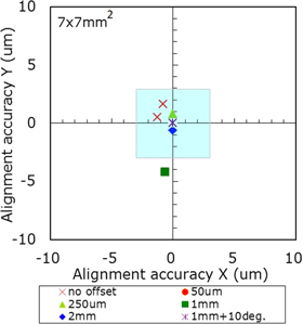
Figure 16. Self-alignment accuracy of chips. © 2012 IEEE. Reprinted, with permission, from [50].
Download figure:
Standard image High-resolution imageIn case of 'face-up' die bonding by means of self-alignment, the electrical interconnection must be completed in a successive process step. This could be realised by embedding of the chip-on-film assemblies in a patternable polymer layer followed by opening of contact pads and fabrication of a thin film metal redistribution layer. We have successfully demonstrated such an interconnection scheme, however, not yet in combination with self-aligned chips [26].
By transferring these experimental results to R2R die bonding, a fast running and highly accurate process for component placement could be established. Such a process would exhibit the following principal benefits: (a) die feeding could be realised at several bonding sites in parallel by rather simple mechanical tools, (b) self-alignment of chips can be accomplished during web movement from one station to another and (c) curing of adhesive could be done in a continuous mode without further mechanical control of the die position.
4.2. Assembly of off-the-shelf components
Another method of hybrid integration on foils involves commercially available, SMD components. As with traditional PCB integration, hybrid integration of SMD components on film substrates requires the SMD components to be electrically connected to the wiring lines on the film substrate to realise the system functionality. To accomplish this integration, contact pads on the wiring foil should be free from passivation and they should have a size as well as format similar to those of the SMD components. Both standard SMDs and flexible components are assembled at Fraunofer EMFT with a three-axis gantry equipped with a rotating tool holder, three dispensing systems and movable cameras. This equipment enables versatile, automated pick-and-place procedure by which different pick-up tools are collected, changed and returned to their stand-by positions. A R2R conveyor system transports the film web over a foil-processing table that includes room temperature processing zones in addition to hot processing areas.
The assembly involves a pick-and-place method that is described as follows. The process starts with the precise dispensing of a conductive adhesive on the contact pads on the film prior to placing the SMD components. The exact positions of the pads were registered by the image recognition system, which was used for accurate positioning. Then, the pick-and-place step was performed by a pick-up tool that was compatible in size with that of the parts to be picked. The SMDs were first picked up from the supplying position and then placed on their respective contact pads. The placement accuracy of the components was in the range of ±25 μm. After that, the dispensed silver-filled adhesive was cured to facilitate the required electrical connection and mechanical stability. The curing step was performed while the R2R web was conveyed from the bonding station further onto the hot plate area. If the curing of the adhesive bonding the SMDs requires to be performed at temperatures above room temperature, this assembly step must be executed before assembling any temperature-sensitive element, for example electrochromic displays. Though room temperature curing is possible, it increases the overall processing time considerably. The bonding force of the polymer adhesive gluing the SMDs to the film is lower than that of conventional solder pastes. In addition, it should be noted that the film substrate is flexible whereas the assembled SMD parts are rigid. Besides, due to their greater height, the SMDs stick out on the film surface and therefore any intense bending or twisting can detach the SMDs from the pads even after curing of the adhesive. Hence, in order to offer a good level of protection to the SMD components from mechanical stress, an encapsulating layer was placed locally by dispensing a transparent, epoxy-based glob top over the SMDs. Thermally curable glob tops are not optimal as high temperatures could introduce thermal stress on the assembly which could warp and shrink the films that could lead to delamination of the components. Thus, to avoid any thermal stress and to minimise the curing time, a low temperature fast curing or an UV curing material could be utilised. Figure 17 portrays the final assembly consisting of resistors and capacitors in 0603 format (1600 × 800 μm), two transistors and an IC in quad-flat no-leads (QFN) package mounted on 50 μm thick PET film.
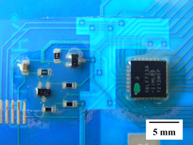
Figure 17. Pick-and-place assembled SMD components on PET film.
Download figure:
Standard image High-resolution image5. 3D integration of foils
Similar to 3D stacking of silicon chips, foil substrates can also be stacked on top of each other to reduce the surface area of the system. The procedure followed to achieve such 3D foil stacks is illustrated in figure 18. The process involves two foils, foil 1 (sheets) and foil 2 (roll). Hence, the 3D integration of foils can be considered as a semi-R2R process. One side of the foils were patterned with conductive wiring lines achieved using the screen printing process described in section 3.1. The first step in the process of foil-to-roll attachment is the lamination of a pressure sensitive adhesive (PSA) tape on foil 1, which allows for low temperature gluing. Then, the foil stack to be assembled on top (foil 1 in this case) consisting of foil 1 and adhesive tape was drilled with a laser to create via holes. Next, the via drilled stack consisting of foil 1 and the adhesive tape were placed precisely on top of foil 2 roll using image recognition and then, the two foils were glued together by applying required bonding pressure. After the foils were bonded together by the PSA, precise dispensing and curing of a silver-filled conductive adhesive into the via holes was performed using the gantry system to complete the process. One specific requirement for creating these 3D foil stacks is that the via holes must be large enough to allow the viscous conductive adhesive to flow in and fill the holes. Therefore, we opted for via holes having a diameter of 500 μm. The assembly line used for the foil-to-roll stacking process is shown in figure 19. The semi-R2R procedure of foil stacking can also be applied for mounting films on conventional and flexible PCBs. Likewise, the process can also be implemented for the integration of other flexible components such as printed batteries and displays on films. The throughput of film pick-and-place mounting could be as high as 1000 pieces h−1. For bonding the flexible components on films, an adhesive stripe matching the pad size and geometry of the flexible components can be cut by a laser and then the parts can be affixed to the film surface. The main restriction for this process is that higher curing temperatures should be avoided since several flexible components, such as electrochromic displays and printed batteries rapidly degrade above 100 °C. Therefore, the curing of the conductive adhesive should be performed at room or moderate temperatures, which consequently reduces the process speed. For multi-layered stacks, the use of room temperature curing adhesives might limit the speed of R2R processing as considerable drying time is needed before the foil roll can be spooled in again for stacking the next layer.
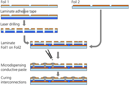
Figure 18. Process schematic for 3D integration of films.
Download figure:
Standard image High-resolution image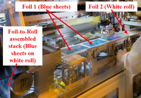
Figure 19. Foil-to-roll assembly of films.
Download figure:
Standard image High-resolution image6. Application example—hybrid integrated flexible temperature sensor label
Figure 20 shows a temperature sensor label manufactured using the hybrid integration process constituting of screen printing, assembly of SMD components and 3D integration of foils described in the previous sections. The screen printing steps enumerated in section 3.1 were applied to pattern the different layers of the system such as the wiring lines, dielectric and passivation layers. On the 215 mm wide band, three labels were assembled per band segment. The assembled SMD components provide the sensor and electronic logic functions of the label. When the label is placed on the sample whose temperature is to be measured, the SMD thermistor assembled on the label detects the temperature, which is then displayed on the electrochromic display. Three SMD light emitting diodes connected on the label indicate proper functioning of the system. The electrochromic display and the two printed batteries were separately supplied with their respective double-sided pressure tape, before they were transferred to the backside of the substrate for pick-and-place assembly.

Figure 20. Hybrid integrated temperature sensor label.
Download figure:
Standard image High-resolution imageSilver-filled adhesive was dispensed into the via holes from the topside of the substrate until the adhesive reached the underlying pads of the batteries and display. An additional foil component acting as the ON/OFF switch for the system was screen-printed, which when pressed establishes contact with the underlying open wiring, thereby closing the electronic circuit and the temperature is displayed on the electrochromic display. Some key specifications of the components of the temperature sensor label are mentioned in table 2.
Table 2. Key specifications of components of the flexible temperature sensor label.
| Component | Key specifications |
|---|---|
| Electrochromic display | 2 × 7 segments; reduction voltage: 3 V; oxidation voltage: 2.5 V; hold time: 6 s |
| Flexible battery | Voltage: 3 V; minimum initial capacity: 10 mAh; operating temperatures: −35 °C to 50 °C; operating humidity: 20%–90 %RH |
| Negative temperature coefficient thermistor | 100 kΩ; SMD size: 0603; operating temperature: −40 °C to 125 °C |
| Microcontroller | 8-bit-MCU UQFN 28-pin |
| Foils used | Substrate: PET; top protection foil: PEN |
7. Fatigue reliability of R2R micro-fabricated wiring lines
The fundamental advantages exhibited by flexible electronics over traditional electronics are their conformability and bendability. Many applications require a one-time bendability, which relaxes requirements considerably. However, there are also applications where electronic components are bent during their entire life cycle. Therefore, different flexible electronic systems have different requirements that have to be considered during development and testing. In line with these targets, we conducted fatigue reliability experiments on COF assemblies fabricated using PI foils with 4 μm thick electroplated copper wiring lines. The custom-built test equipment utilised for the experiments is shown in figure 21. The bending tester facilitated online measurement of electrical characteristics during repeated bending cycles. The test equipment consists of two main components, a fixed platform and a movable arm. The fixed platform comprises of four PCBs with connectors to link with the electrical measurement unit. Subsequently, to each of the PCBs, one test sample can be attached for bending either at a defined bending radius or at free-form bending. One end of the test samples was attached to the PCBs while their other end rested on the movable arm that moved up and down causing the samples to bend. The PCBs were in turn connected to a parameter analyser (HP 4156C) that offered high precision resistance measurements down to micro Ohms. Comprehensive explanation about the test equipment and the test protocol have been elaborated in our earlier papers [48, 51]. The cyclic procedure followed for the bending test consists of four sequential steps as mentioned below.
- 1.0° start position.
- 2.Bending from 0° to 90°.
- 3.90° rest position.
- 4.Bending from 90° to 0°.

Figure 21. Test equipment used for fatigue reliability analysis. © 2016 IEEE. Reprinted, with permission, from [51].
Download figure:
Standard image High-resolution imageWe conducted recurrent bending tests on COF assembly samples with ultra-thin silicon chips fabricated using flip-chip bonding explained in section 4.1.1. The collective objective of the experiments was to characterise the repeated bending reliability of the thick film copper wiring lines as well as that of the mounted ultra-thin chip. The resistance of the daisy chain structures on the chips was measured continuously and it was used as the criteria to identify the failure of the COF assembly happening due to delamination of chip from the foil substrate, chip cracking and rupture of wiring lines. During repeated bending, the daisy chain resistance increased slowly after 2500 bending cycles before surging drastically after 3200 bending cycles. Then, the samples were analysed optically, which revealed a series of cracks on the electroplated copper wiring lines (figure 22). However, no other mechanical damage such as chip cracking, delamination of the chip from foil and delamination or cracks on the chip bump pads at the chip-foil bonding interface was observed. In order to reinforce the foil wiring lines by moving them closer to the neutral stress plane (plane experiencing zero stress during bending), an encapsulation layer was laminated on top of the COF assemblies. Such encapsulated COF assemblies endured the bending tests up to four times longer before the appearance of first signs of wiring line rupture (figure 23). Thus, it can be concluded that encapsulation offered a significant reinforcement for the wiring lines against bending stress. Figure 23 compares the daisy chain resistance behaviour of COF assemblies (with and without encapsulation) during repeated bending at a bending radius of 5 mm. We also conducted fatigue reliability tests on flexible 28 μm thin chips and rigid 250 μm thick chips. Free-form bending was implemented for these samples since the rigid 250 μm thick chips cannot be bent and hence the influence of the chip rigidity on the fatigue reliability of wiring lines was analysed. As expected, chip thickness was the deciding factor in this case where the COF assembly with thinner 28 μm chip survived 6000 bending cycles whereas the COF assembly with thicker 250 μm chip failed after 3650 bending cycles (figure 24). Similar to fixed radius bending tests, the cracking of wiring lines was the sole cause of failure. However, it should be noted that rupture of wiring lines during repeated bending is not limited only to micro-fabricated wiring lines since cracking of screen-printed silver wiring lines has also been reported in literature [52]. Thus, it is evident that irrespective of the process of manufacturing, rupture of wiring lines will significantly degrade the performance of the entire flexible electronic system that could cause irrecoverable failure of the system. Therefore, exhaustive research should be devoted to understand the bending dynamics of the wiring lines on films fabricated using diverse techniques and to explore ways to improve the reliability of metallised patterns before implementing these metal patterning approaches for R2R mass production of film based flexible electronics.
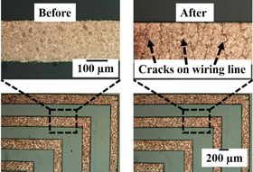
Figure 22. Cracks on wiring lines due to repeated bending. © 2016 IEEE. Reprinted, with permission, from [51].
Download figure:
Standard image High-resolution image
Figure 23. Daisy chain resistance of 12 μm chip-on-foil assemblies under repeated bending at a bending radius of 5 mm.
Download figure:
Standard image High-resolution image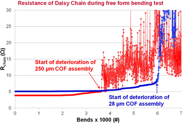
Figure 24. Resistance of daisy chain of 28 and 250 μm COF assemblies during free-form bending tests. © 2016 IEEE. Reprinted, with permission, from [51].
Download figure:
Standard image High-resolution image
8. Conclusion and outlook
The emerging interest in flexible electronics for the ever-increasing consumer application cases urges the research community for high performance solutions at low cost. This objective could be accomplished relatively faster and efficiently if organic and inorganic materials go hand-in-hand by complementing each other to produce hybrid integrated flexible electronics. We have emphasised the requirements and benefits of such hybrid integrated flexible electronic systems over isolated organic and inorganic solutions. Two diverse R2R approaches to manufacture wiring layers on film substrates required for hybrid integration were explained in detail. Furthermore, hybrid integration techniques for integrating flexible bare silicon chips and conventional SMDs on film substrates were elaborated. The integration processes for flexible bare silicon chips on films is still a novel concept with several open questions. Therefore, it is plausible to conduct extensive experiments on sheet level until in-depth cognisance of various materials and processes utilised for the integration process is established. Later on, the integration process can be transferred to R2R platforms. Besides, a semi-R2R process followed for 3D integration of films was also described. In addition, an application example (temperature sensor label) fabricated using hybrid integration on R2R processed film substrates was demonstrated. Finally, fatigue reliability studies of R2R fabricated wiring lines revealed the enhancement of mechanical robustness of the wiring lines due to encapsulation as well as the influence of chip rigidity and thickness on the fatigue reliability of the wiring lines.
With the advances in information and communication technology coupled with the improvements in sensors and actuators for the next generation devices for the IoT and Industry 4.0, a wide spectrum of possibilities is available for flexible electronics. When the high performance features of inorganic electronics are supplemented by the conformability of plastic film substrates, the merger results in hybrid integrated flexible electronics. However, the real benefits of film based flexible electronics could be enjoyed only when the entire hybrid integration technology is transferred to a continuous R2R process. Therefore, our next steps are focussed towards further deepening the know-how we have acquired until now to a level substantive for introducing R2R processing at all process stations. We primarily aim to address challenges in R2R film processing arising from the dimensional changes in film substrates due to non-uniform web tension and repeated thermal treatments.
Acknowledgments
The authors are grateful for the financial support offered by the European Commission, the Bavarian Government and the German Federal Ministry of Education and Research in numerous research projects. The authors extend their thanks to Martin König, Indranil Bose, Robert Faul, Erwin Yacoub-George, Waltraud Hell, Dieter Bollmann and Andreas Drost for their technological contributions.