


Abstract
All inkjet printed rectifying diodes based on a metal-insulator-semiconductor (MIS) layer stack are presented. The rectifying properties were optimized by careful selection of the insulator interlayer thickness and the layout structure. The different diode architectures based on the following materials are investigated: (1) silver/poly (methylmethacrylate-methacrylic acid)/polytriarylamine/silver, (2) silver/polytriarylamine/poly (methylmethacrylate-methacrylic acid)/silver, and (3) silver/poly (methylmethacrylate-methacrylic acid)/poly-triarylamine/poly(3,4-ethylenedioxythiophene) poly (styrenesulfonate). The MIS diodes show an averaged rectification ratio of 200 and reasonable forward current density reaching 40 mA cm−2. They are suitable for a number of applications in flexible printed organic electronics.
Export citation and abstract BibTeX RIS
1. Introduction
Inkjet printing is a well accepted deposition technology for functional materials in the area of printed electronics [1–12]. It allows the precise deposition of patterned functional layers on both rigid and flexible substrates. Furthermore, inkjet is considered to be an up-scalable deposition technology for industrial applications [13, 14]. Inkjet printing enables the manufacturing of devices e.g. schottky diodes that are considered as one of the simplest electronic devices in the semiconductor industry [15–19]. They produce high current density, low forward voltage drops and fast switching behaviour [15–19]. The electrode materials that can always be considered are e.g. silver (bulk work function: 4.26 to 4.74 eV), copper (bulk work function: 4.53 to 4.98 eV), aluminium (bulk work function: 4.06 to 4.28 eV), poly (3,4 ethylenedioxythiophene) poly (styrenesulfonate) (PEDOT:PSS, bulk work function: 5.1 eV) [20, 21]. Either one of these functional conductive materials look simple to process, but in most of the cases it is challenging to appoint and locate them (having different work functions) adjacent to the semiconductor interface layer [22]. Recently, it has been reported that MIS structures show a rectifying behaviour [23–26]. In the inorganic MIS devices where the conventional insulating silicon dioxide (SiO2) thickness is below 7 nm, the charge carriers can tunnel through the insulating barrier [27, 28]. This causes a reduction in the reverse saturation current and an increase in the barrier height in the energy band diagram [27, 28]. On the contrary, a thick insulating layer with 50 to 200 nm will block the charge carrier flow and will not show rectification [26]. However, if the insulator layer is leaky due to an irregular morphology produced by the mutual interaction/blend of the semiconductor to insulator interfaces it can lead to a voltage controlled leakage and to corresponding asymmetric current versus voltage curves [22]. Herein, we focus on assessing the electrical characteristics of MIS based diodes fabricated completely by inkjet printing technology. The complete layer stack consists of: (a) top and bottom printed conductive layers using a silver nano-particle ink and in other case PEDOT:PSS, (b) a polymeric insulator layer using poly (methylmethacrylate-methacrylic acid in ethtyl lactate) MMAcoMAA and (c) a polymeric polytriarylamine PTAA semiconducting layer. Due to the interaction between the MMAcoMAA and the semiconductor a MIS diode is obtained showing a rectifying behaviour [22]. Moreover, the yield of the MIS diode devices will be studied to ensure a reliable technology.
2. Experimental
2.1. Fabrication and characterization
Three types of MIS diode architectures are reported here. The schemes for the MIS diode architectures are shown in figure 1. Inkjet printing of MIS diodes was conducted based on the architecture mentioned in figure 1. Silver nanoparticle ink from SunTronic EMD 5603 (SunChemical), PEDOT:PSS ORGACON™ IJ-1005 (Agfa-Gevaert N.V.), MMAcoMAA from (MicroChem Corp.) and PTAA p-type organic semiconductor (FS0027, from Flexink Ltd) were used as the functional inks for manufacturing these MIS diodes on a heat stabilized 125 μm thick polyethylene naphthalate (PEN) Teonex Q65FA substrate from Dupont Teijin Films.

Figure 1. Schematic diagrams for the different MIS diodes (a) Architecture no. 1, (b) Architecture no. 2, and (c) Architecture no. 3.
Download figure:
Standard image High-resolution imageThe inkjet printing of the functional layers was performed using the Dimatix Material Printer DMP-2831 from Fujifilm Dimatix Inc. using standard development printheads (DMC) with 10 pL nominal drop volume. For Architecture no. 1, printing was performed solely for bottom silver and MMAcoMAA layers. For Architecture no. 2 and Architecture no. 3, the entire layer stacks were inkjet printed. Table 1 shows an overview of the printing methodology, printing parameters as well as curing/sintering parameters for the individual functional layer used for manufacturing the MIS diodes. The aim to use PEDOT:PSS as an anode was to achieve an semi-organic diode by means of replacing the bottom silver electrode.
Table 1. Overview of printing and curing/sintering parameters.
| Layer Sequence | 1st | 2nd | 3rd | 4th | ||
|---|---|---|---|---|---|---|
| Architecture no. 1 | Deposition process | Inkjet Printing Technology | Inkjet Printing Technology | Drop Casted | Drop Casted | Partially inkjet printed MIS diodes |
| Layer | Bottom electrode (silver) | Barrier layer (MMAcoMMA) | Organic semiconductor (FS0027) | Top electrode (silver) | ||
| Number of layers | 1 | 1, 3, 6, 12 | 1 | 1 | ||
| Drop space (μm) | 20 | 20 | — | — | ||
| Pattern size (mm × mm) | 7 × 5 | 5 × 5 | — | Approximately 25 | ||
| Post-treatment in hot plate (min, °C) | 20, 120 | 60, 150 | 20, 100 | 20, 120 | ||
| Architecture no. 2 | Deposition process | Inkjet Printing Technology | Inkjet Printing Technology | Inkjet Printing Technology | Inkjet Printing Technology | All inkjet printed MIS diodes |
| Layer | Bottom electrode (silver) | Organic semiconductor (FS0027) | Barrier layer (MMAcoMMA) | Top electrode (silver) | ||
| Number of layers | 1 | 2 | 1, 3, 6, 12 | 2 | ||
| Drop space (μm) | 20 | 20 | 20 | 20 | ||
| Pattern size (mm × mm) | 7 × 5 | 5 × 5 | 4 × 4 | 3 × 3 | ||
| Post-treatment in oven (min, °C) | 30, 135 | 20, 100 | 60, 150 | 30, 135 | ||
| Architecture no. 3 | Deposition process | Inkjet Printing Technology | Inkjet Printing Technology | Inkjet Printing Technology | Inkjet Printing Technology | All inkjet printed MIS diodes |
| Layer | Bottom electrode (PEDOT:PSS) | Organic semiconductor (FS0027) | Barrier layer (MMAcoMMA) | Top electrode (silver) | ||
| Number of layers | 1 | 2 | 1, 3, 6, 12 | 2 | ||
| Drop space (μm) | 10 | 20 | 20 | 20 | ||
| Pattern size (mm × mm) | 7 × 3 | 4 × 4 | 5 × 5 | 3 × 3 | ||
| Post-treatment in oven (min, °C) | 6, 120 | 20, 100 | 60, 150 | 30, 135 | ||
For all of the three MIS diode architectures, the thickness of the MMAcoMAA layer was varied incrementally to study the effect of the rectification. This was done by changing the number of layers, but keeping the drop space constant. The active area for the MIS diodes (for Architecture no. 2 and Architecture no. (3) was kept constant. After fabricating the MIS diodes, the layers were optically characterised with light microscopy Leica DM 4000 M and by scanning electron microscopy (SEM) processed with focused ion beam (FIB) cut. Subsequently, the MIS diodes were electrically characterized using a Keithley 2636A source meter connected to a Suess mess probe station. Positive voltages (forward bias) refers to the top silver electrode for all the architectures. All electrical measurements were performed under ambient conditions.
3. Results
3.1. Optical analysis
Figure 2 depicts the microscopic images and photographs for the three MIS diode architectures. Through the microscopic image and also the photograph, the MIS diode from Architecture no. 1 shows a top silver layer which has been drop casted and which has no definite form. Due to the stacked position of the layer in this architecture, it was seen that the drop casted top silver electrode exhibited contraction in its dimension. Also, it was detected that the shape for the drop casted top silver is irregular due to the process of the deposition itself and the low surface energy possessed by the FS0027 organic semiconductor layer.

Figure 2. Microscopic images and photos of the MIS diodes for (a) Architecture no. 1, (b) Architecture no. 2, and (c) Architecture no. 3.
Download figure:
Standard image High-resolution imageIn contrast to this, Architecture no. 2 is an all-inkjet printed MIS diode. A microscopic image for the fabricated diode can be seen in figure 2(b) at the corner involving 3 layers (as an example) of MMAcoMAA. The other layers which constitute the MIS diode can be also seen, such as the bottom silver electrode, FS0027 organic semiconductor and the top silver electrode. The basic difference in this architecture can be found in the position of the MMAcoMAA and the FS0027 organic semiconductor layer. They are interchanged, so as to facilitate improved wetting of the silver ink and therefore the printing process to complete the diode layer stacks. Although it was seen that the layer formations (MMAcoMAA) for the fabricated diode are not very uniform. This characteristic behaviour of the layer arrives from the subsequent drying procedure of the ink during the printing process. This characteristic inhomogeneity is then transferred to the next succeeding layer until it reaches the top silver electrode. Occasionally, de-wetting of the silver ink (for the top electrode) was observed which refers to the high quantitative involvement of the MMAcoMAA layer with FS0027 organic semiconductor with respect to the printed area. For the final Architecture no. 3, a microscopic image can be seen for the MIS diode, again involving 3 layers MMAcoMAA. Due to the high smoothness of the PEDOT:PSS layer, the next stacked succeeding layers were expected to show similar and improved layer formation. This behaviour can be directly seen in the depicted microscopic images. The silver electrode is also found to exhibit better wetting and contribute to good layer formation. Although occasionally again, the layer formation was seen to be disturbed, but this is due to the high quantitative involvement of the MMAcoMAA material. In addition to this, SEM images were also taken for the analysis of the layer internally through the cross section of the printed layers which is made by a FIB cut. The FIB cut was made across the printing direction for the fabricated MIS diodes. Figure 3 gives an overview of the inkjet printed layers. Figure 3(a) shows the layer stack of the PEDOT:PSS and FS0027 organic semiconductor (from bottom to top) and figure 3(b) silver and MMAcoMAA layers (from bottom to top).

Figure 3. SEM images of the cross-section containing (a) PEDOT:PSS and FS0027 (bottom to top), and (b) silver and MMAcoMAA (bottom to top).
Download figure:
Standard image High-resolution imageAs the analysis of the layer quality and thickness reveals, the printed layers were seen to bind together without any definite interfaces which can be caused during the printing process. But in figure 3(b) some air bubble like structures were detected which can be the cause of the deposited ink and the subsequent drying of the layer itself. We believe that during the jetting process some air bubbles are generated and these bubbles get trapped once the drying phenomenon already starts internally during the printing phase. For the analysis, single printed layers for each individual material were considered but with different drop spaces (optimal value necessary to obtain a continuous and smooth layer). The used drop space for the printing of these PEDOT:PSS, silver, MMAcoMAA and FS0027 layers were 10 μm, 20 μm, 20 μm and 20 μm respectively. The average thicknesses from the individual PEDOT:PSS, silver, MMAcoMAA and FS0027 layers were found to be 0.6 ± 0.01 μm, 0.3 ± 0.01 μm, 1.7 ± 0.02 μm, and 0.7 ± 0.03 μm respectively. The thickest value can clearly be detected from the printed MMAcoMAA layer. It can also be concluded that the total thickness of the MIS diodes in Architecture no. 2 and Architecture no. 3 will vary according to the number of MMAcoMAA layers which is printed furthermore.
3.2. Electrical analysis
The analysis of the electrical characteristics for the printed MIS diodes for the different architectures was performed on the basis of current density versus voltage (J–V) curves. The measurements are based on the obtained current modulations when the different voltage values are biased on the fabricated MIS diodes (step of 1.0 V, applied from +10.0 V to −10.0 V). Every time, 20 MIS diode samples are considered from each diode architecture. The optimal results based on the tendency of the diodes (out of 20 samples) and with respect to the three architectures are considered here. On the basis of these results, a rectification ratio is also calculated. The rectification ratio here can be defined as the proportion (ratio) of the obtained current at the biased positive to the negative of the same voltage (modulus). The values for the quantity and stability of the rectification ratio will define the quality of the diode and its short term reliability. In addition to this, cumulatively the fabrication yield and performance of the MIS diodes are derived for the all inkjet printed diode architectures.
3.2.1. Architecture no. 1
Figure 4 shows the J–V curve for the MIS diodes comprising of Architecture no. 1. The different characteristics correspond to the use of several interlayer thickness constituting 1 layer, 3 layers, 6 layers, and 12 layers of MMAcoMAA respectively. For the diodes having 1 layer of MMAcoMAA, the maximum (max) forward current density (current at positive voltage for the defined active area) is seen to reach 300 μA cm−2 at +10.0 V, whereas at −10.0 V the reverse current density (current at negative voltage for the defined active area) can be seen to reach 0.1 μA cm−2. This low value exhibited here is preferable for low leakage current and better diode performance. Persistently, the working of the diode is exhibited with the quantity of current in several tens towards hundreds of μA cm−2.
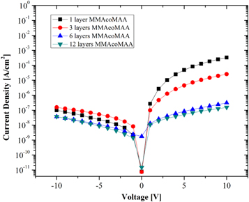
Figure 4. Graph showing a characteristic J–V curve for MIS diodes as function of MMAcoMAA layers (Architecture no. 1).
Download figure:
Standard image High-resolution imageFor the diodes with 3 layers of MMAcoMAA, the highest forward current density is 20 μA cm−2 at +10.0 V, and 0.15 μA cm−2 in reverse current at −10.0 V. The working of the diode is exhibited at the forward voltage regime with the quantity of current density tending towards few μA cm−2. Similarly, the diodes having 6 layers of MMAcoMAA, the max obtained forward current density is 0.3 μA cm−2 at +10.0 V, and 40 nA cm−2 in reverse current density at −10.0 V. In this case, the difference in the quantity of the obtained current at the forward and reverse direction was found to be minimum (min), although the reverse current or the leakage current is found to be similar. For the diodes with 12 layers of MMAcoMAA, the max obtained forward current density is 0.16 μA cm−2 at +10.0 V, and 40 nA cm−2 in reverse current density at −10.0 V. The values of current at both the forward and reverse regime are found to be low in quantities. A definite dip in the values for the forward current is seen when the diodes are compared with respect to the increasing number of MMAcoMAA layers. The shape of the curves depicted here can also be seen to flatten out on both the voltage regimes for the diodes containing 6 and 12 layers of MMAcoMAA. The best diode characteristic is obtained from 1 layer and 3 layers of MMAcoMAA.
3.2.2. Architecture no. 2
In figure 5, a J–V curve is shown for the MIS diodes comprising of Architecture no. 2. For the diodes with 1 layer of MMAcoMAA, the max obtained forward current density is 6 μA cm−2 at +10.0 V, and 70 nA cm−2 in reverse current density at −10.0 V. Again this obtained low and high value of the current densities at the reverse and forward regime for the applied voltage result in good rectification. For the diodes with 3 layers of MMAcoMAA, the max obtained forward current density is 0.7 μA cm−2 at +10.0 V, and 10 nA cm−2 in reverse current density at −10.0 V. On the contrary, for the diodes with 6 layers of MMAcoMAA, the max obtained forward current density is 40 nA cm−2 at +10.0 V, and 0.2 nA cm−2 in reverse current density at −10.0 V.

Figure 5. Graph showing a characteristic J–V curve for MIS diodes as function of MMAcoMAA layers (Architecture no. 2).
Download figure:
Standard image High-resolution imageSimilar characteristic results were obtained for the diodes with 12 layers of MMAcoMAA, with 90 nA cm−2 and 0.3 nA cm−2 current densities in the forward and reverse voltage regime. A dip in the values for the forward current density is seen when the diodes are compared with respect to the increasing number of MMAcoMAA layers. In both cases, for the diodes with 6 and 12 layers of MMAcoMAA, the quantity of the max reverse current density detected is extremely low, but so is the max forward current. The shape of the J–V curve is more ideal for the condition where the diode contains 1 layer and 3 layers of MMAcoMAA. The shape of the curves depicted here do not flatten out at all. The best diode characteristic is obtained again from 1 layer and 3 layers of MMAcoMAA.
3.2.3. Architecture no. 3
In figure 6, a J–V curve is shown for the MIS diodes comprising of Architecture no. 3. For the diodes with 1 layer of MMAcoMAA, the max obtained forward current density is 3 mA cm−2 at +10.0 V, and 20 μA cm−2 in reverse current at −10.0 V. The diodes having 3 layers of MMAcoMAA, the max obtained forward current is 40 mA cm−2 at +10.0 V, and 0.2 mA cm−2 in reverse bias at −10.0 V. On the contrary, for the diodes with 6 layers of MMAcoMAA, the max obtained forward current is 50 μA cm−2 at + 10.0 V, and 0.8 μA cm−2 in reverse current at −10.0 V. Similarly, for the diodes with 12 layers of MMAcoMAA, the max obtained forward current reaches 20 mA cm−2 at +10.0 V, and 30 μA cm−2 in reverse current at −10.0 V. There is a dip in the values for the forward current when the diodes are compared with respect to the increasing number of MMAcoMAA layers. In all the cases for this diode architecture, the quantity of the max reverse saturation current detected is high (in μA) and so is the max forward current (in mA). The curves do not flatten out on both the forward and reverse voltage regimes. The best diode is obtained from 1 layer and 3 layers of MMAcoMAA (considering best stability and highest forward current density).
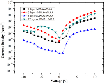
Figure 6. Graph showing a characteristic J–V curve for MIS diodes as function of MMAcoMAA layers (Architecture no. 3).
Download figure:
Standard image High-resolution imageThe function of the varying MIS diode architectures against the thickness of the MMAcoMAA barrier layer for the swept voltage range is analysed. the rectification ratio versus biased voltages can be observed in three parts for 1 layer, 3 layers, 6 layers and 12 layers of MMAcoMAA. The first, second and third part gives an overview for Architecture no. 1, Architecture no. 2 and Architecture no. 3, respectively.
It was found that for Architecture no. 1, max and min values for the rectification ratios considering that 1 layer of MMAcoMAA involved in the diode layer stack were between 3311.5 (3312 approx.) to 121.6 (122 approx.), respectively), with a difference of 3190 approx.; considering 3 layers of MMAcoMAA between 164.4 (164 approx.) to 12.1 (12 approx.) with a difference of 152 approx.; considering 6 layers of MMAcoMAA between 314 to 2.6 (12 approx.) with a difference of 311 approx.; and considering 12 layers of MMAcoMAA between 2320.3 (2320 approx.) to 4.2 (4 approx.) with a difference of 2316 approx. When all the values corresponding to this architecture are analysed at the end, it could be concluded that for Architecture no. 1 and including 1 layer and 3 layers a trend toward the increasing rectification ratio is given. But similarly, for the same architecture and the diodes containing 6 and 12 layers of MMAcoMAA, disturbances at the beginning of the voltage biasing are evident. These disturbances could be explained by the behaviour of the low reverse and relatively high forward current at low voltage (around 2 V to 3 V). The best resulting diode can be obtained from the stack where the number of MMAcoMAA layers is 1.
As for Architecture no. 2, max and min values for the rectification ratios considering that 1 layer of MMAcoMAA involved was between 107 approx. to 2 approx., respectively, with a difference of 105 approx.; considering 3 layers of MMAcoMAA between 116.7 (117 approx.) to 1.7 (2 approx.) with a difference of 115 approx.; considering 6 layers of MMAcoMAA between 175.3 (175 approx.) to 8.5 (9 approx.) with a difference of 167 approx.; and considering 12 layers of MMAcoMAA between 536.4 (536 approx.) to 5.1 (5 approx.) with a difference of 531 approx. When all the values corresponding to the different number of MMAcoMAA layers are considered among themselves for a particular diode architecture, then an increasing trend can be seen with a minimum amount of difference. Since the values for the rectification ratios obtained among the same kind of diodes themselves are very close to each other, therefore they are stable. The best resulting diodes can be obtained from the stack where the number of MMAcoMAA layers is 1 and 3.
For the last Architecture no. 3, max and min values for the rectification ratios considering that 1 layer of MMAcoMAA involved was between 219.7 (220 approx.) to 4.2 (4 approx.) respectively, with a difference of 216 approx.; considering 3 layers of MMAcoMAA between 182.1 (182 approx.) to 17.4 (17 approx.) with a difference of 165 approx.; considering 6 layers of MMAcoMAA between 321.4 (322 approx.) to 0.5 (1 approx.) with a difference of 321 approx; and considering 12 layers of MMAcoMAA between 528.4 (529 approx.) to 0.6 (1 approx.) with a difference of 528 approx. When all the values corresponding to the different number of MMAcoMAA layers are considered among themselves for this diode architecture, then an increasing trend can be seen with a large amount of disturbances. The best resulting diode can be obtained from the stack where the number of MMAcoMAA layers is 3.When all the curves are considered with regards to all the mentioned architectures and also the number of MMAcoMAA layers then it can be said that the best diode can be fabricated using 1 or 3 layers of MMAcoMAA in function of the voltage applied to the device.
For the second condition, the rectification ratios concerning the average value and their standard deviation are considered. In this section, the quantity of deviation is also considered which will indicate the stability of the diodes. The average values for the rectification ratio of the diodes for Architecture no. 1 for the different MMAcoMAA layers involved are as follows: 1 layer: 1820 ± 1299, 3 layers: 84 ± 58, 6 layers: 35 ± 93 and 12 layers: 252 ± 696 respectively. Similarly, the average rectification ratio for the diodes belonging to Architecture no. 2 containing a different number of MMAcoMAA layers are as follows: 1 layer: 42 ± 37, 3 layers: 54 ± 45, 6 layers: 60 ± 50 and 12 layers: 111 ± 169 respectively. And, for the diodes belonging to Architecture no. 3 containing a different number of MMAcoMAA layers are as follows: 1 layer: 124 ± 86, 3 layers: 111 ± 58, 6 layers: 133 ± 122 and 12 layers: 125 ± 192 respectively. As a conclusion for the results, for all the architectures and 12 layers of MMAcoMAA involved, the amount of the standard deviation observed is the highest. Therefore, these diodes cannot be totally reliable. The reasons can be predicted from the high amounts of MMAcoMAA material deposited and thereby its strong interaction with the semiconductor layer. For Architecture no. 1, the best result for the diodes can be seen when the number of MMAcoMAA layers is 1. Even though the diodes exhibit the highest standard deviation, it also shows the highest rectification ratio (average value). The reason for this high deviation can be due to low performance at low voltages. For the diodes which are all inkjet printed belonging to Architecture no. 2, the best results can be seen when the number of MMAcoMAA layers is 3. The diodes show the maximum rectification ratio (average value) and comparatively the lowest standard deviation. Again for the diodes which are all inkjet printed belonging to Architecture no. 3, the best result for the diodes can be seen when the number of MMAcoMAA layer is 1. The diodes show relatively good rectification ratio (average value) and also low standard deviation.
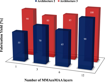
It is believed that the physics behind the functionality of the MIS diode lies inside the stack of materials itself. It is known that when there is a deposition of one layer over the another layer (especially in a solution processing technique e.g. inkjet printing of the individual layers), the solvents and the polymer contents in the liquid state might interact with the cured layer beneath. The most interesting interaction is the FS0027 semiconductor to MMAcoMAA insulator interface. In this condition, it can be also expected that several networks might form and they might also contain polymers from counter interface layers e.g. formation of micro to nanoscale FS0027 networks in MMAcoMAA. It is already experienced that MMAcoMAA (being a polymer material with leaky properties) presents a high current through the structure for the forward bias. This explains that with increasing the thickness of the dielectric layer the current decreases, thereby blocking the current. Under reverse bias, the interface of MMAcoMAA and FS0027 is depleted. It is speculated that the junction of the dielectric layer and silver electrode blocks the current, due to the addition of an extra energy barrier in comparison to FS0027, which presents an ohmic contact in the presence of the silver electrode. Because the semiconductor FS0027 is deposited before the MMAcoMAA a network is produced and rectification behaviour is obtained. This demonstrates that apart from the use of a leaky dielectric, it is necessary to create a network among the dielectric semiconductor regardless of the work function of the bottom electrode, i.e. silver or organic polymer. In figure 7, the graphs containing the fabrication yield of the diode samples belonging to Architecture no. 2 and Architecture no. 3 (all inkjet printed MIS diodes) are shown. The focus is based on the architectures and the number of MMAcoMAA layers involved. The calculation for the fabrication yield is made according to two classes: (1) working devices (similar working), and (2) non working or short-circuit or no rectifying diodes. As mentioned earlier, every time 20 samples are considered for Architecture no. 1, the calculated fabrication yield was found to be between 50 to 60% for all the different numbers of MMAcoMAA layers. But, for Architecture no. 2, the fabrication yield was found to be different. The highest fabrication yields of 90% and 70% were achieved for the diodes involving 12 layers and 3 layers of MMAcoMAA. In general, when 1 layer, 3 layers, 6 layers and 12 layers of MMAcoMAA are considered, then the average yield can found to be 70 ± 15%. When only 1 layer, 3 layers and 6 layers of MMAcoMAA are considered then the average yield is found to be 63 ± 8%. The best compromise can be seen for the diodes with 3 layers of MMAcoMAA. But, for Architecture no. 3, the fabrication yield was found to be different. The highest fabrication yields of 100% and 90% were achieved for the diodes involving 12 layers and 1 layer of MMAcoMAA. In general, when 1 layer, 3 layers, 6 layers and 12 layers of MMAcoMAA are considered, then the average fabrication yield can found to be 89 ± 9%. When only 1 layer, 3 layers and 6 layers of MMAcoMAA are considered then the average yield is found to be 85 ± 5%. The best compromise is observed for the diodes with 3 layers of MMAcoMAA. It could be predicted that this high fabrication yield for Architecture no. 3 MIS diodes is because of the involvement of the PEDOT:PSS as an electrode. The material gives a suitably low surface roughness (Ag ∼ 20 nm, PEDOT:PSS ∼ 5 nm) for the development of diodes. Of course, the involvement of more numbers MMAcoMAA layers for both architectures gives the highest fabrication yield for e.g. 12 layers, resulting to diodes which give rise to a low number of electrical short-circuits, but they are more prone to the high quantity of disturbance in terms of the electrical characteristics.
Figure 7. Graph showing the fabrication yield of MIS diodes containing Architecture no. 2, and Architecture no. 3.
Download figure:
Standard image High-resolution image
4. Conclusion
In summary, the electrical properties of rectifying diodes based on a MIS structure were optimized by the proper selection of device architecture and insulator layer thickness. It can be concluded that for MIS diode Architecture no. 1, Architecture no. 2 and Architecture no. 3, the best rectifying diode properties can be achieved when the entire stack includes 1 layer, 3 layers and 1 layer of MMAcoMAA respectively. The decision is made taking into account several diode parameters, namely, the diode property like current density versus voltage characteristic curves, current density, rectification ratios, standard deviations and fabrication yield. From the results, it can be concluded that above a certain dielectric thickness the rectifying properties degrade and the diode becomes resistive between the electrodes and thus the electrical performance decreases. Therefore, the amount of MMAcoMAA layers and the interaction of the FS0027 onto the MMAcoMAA is crucial to obtain a good rectifying behaviour effect. The fabrication yield for achieving good diodes is increased using a smoother layer such as PEDOT:PSS since the work function of both electrodes is not responsible for the rectifying behaviour. It can be reported that these MIS diodes are a new unconventional route for fabricating rectifying diodes. The diodes can be fabricated for various applications with the possibility of using either identical or dissimilar materials for the two electrodes. These types of diodes are all inkjet printed with a fabrication yield of approx. 70 to 80% at atmospheric conditions.
Acknowledgments
This research work was supported by the EU funded project: Technology & Design Kits for Printed Electronics (TDK4PE), grant agreement no.: 287682. The authors for this research work thank TDK4PE for the inspiration, team work, and research performed related to the exploration of functional materials leading to developing new device fabrication routes and the process of inkjet printing. We would also like to thank Mr Dirk Rittrich (Department of Layer Deposition at Fraunhofer ENAS) for his support with SEM analysis.