
Abstract
(CdTe)1-x(In2Te3)x films, with 0.1 ≤ x ≤ 1, were deposited by radio frequency sputtering on glass substrates employing different targets, prepared for each composition. The x-ray diffractograms were consistent with substitutional In incorporation into the CdTe lattice up to a value of x = 0.2. For higher In contents, the films presented structural disorder without reaching full amorphous characteristics. For x = 1, corresponding to In2Te3, preferential growth was observed. The bandgap of the solid solution varied between 1.46 and 1.2 eV, reaching a maximum of 1.58 eV for x = 0.3. For both end binary compounds the random incorporation of a third chemical element produced a significant broadening of the Raman modes consistent with a reduction of the lifetime of the optical phonons. The electrical resistivity was dependent on the Cd concentration reaching a minimum for x = 0.8.
Export citation and abstract BibTeX RIS

Original content from this work may be used under the terms of the Creative Commons Attribution 4.0 licence. Any further distribution of this work must maintain attribution to the author(s) and the title of the work, journal citation and DOI.
Introduction
Cadmium, sulfur, manganese, zinc, mercury or indium when alloyed with tellurium form semiconductors with diverse and important technological applications [1, 2]. Since CdTe is a relatively well studied material, it is natural to take it as precursor in the study of ternary compounds. There are several ternary compounds with proven applications: for instance, HgxCd1-xTe is widely employed for high performance infrared detectors [3]. Indium has been employed to dope CdTe and modify its conductivity [4]; at higher In concentrations and adequate thermodynamic conditions, compounds such as CdIn2Te4 and In2Te3 may be obtained [5]. One of the first studies dealing with the alloy CdInTe was carried out employing bulk crystals yielding the phase diagram of the system (Cd, In, Te) [6].
In regard to technological applications, CdTe is a semiconductor widely employed in the production of commercial solar cells due to its direct bandgap and high optical absorption coefficient. Moreover, CdTe is a material with commercial applications in the detection of high energy radiation [7, 8]. The semiconductor In2Te3, due to its crystallographic structure with ordered vacancies, recently has been considered for diverse applications such as thermoelectricity, ferroelectricity and as anode in lithium-ion batteries [9–11].
Semiconductor thin films are essential to produce devices. Thin film production techniques include sputtering, close space vapor transport, spray pyrolysis, laser ablation, molecular beam epitaxy, among others. The number of reports related to the production of CdTe films is larger [12] than that for In2Te3, InTe and CdIn2Te4 [13–17].
Due to its crystallographic structure In2Te3 belongs to the class of materials termed ordered vacancies compounds, which potentially could incorporate dopants or withstand high radiation doses without suffering major changes in their crystalline structure and, consequently, with the potential for producing electronic devices able to resist harsh environments [18, 19]. Recently, ordered vacancies compounds have attracted large interest as 2D layered compounds capable of improving the efficiency of thermoelectric devices due to weak interlayer van der Waals bonds and strong intralayer bonds [20]. The production of semiconductors with ordered vacancies structure based on CdTe and, among other elements, mercury, gallium, aluminum, and silver have shown an enormous potential in the modification of their electronic properties [21–24]. The formation of alloys between the extremes CdTe and In2Te3 allows not only modifying the bandgap energy between 1.5 and 1.2 eV but also analyzing how the crystal structure is affected [25, 26]. The possibility of modulating the electronic and structural properties using a solid solution of CdTe and In2Te3 is worth studying for technological applications and fundamental material properties.
Radiofrequency sputtering is a versatile technique for obtaining thin films with highly reproducible characteristics in a cost-effective manner. Physical processes during sputtering produce atomic and ionic species of the chemical elements present in the target amenable for the production of alloys. The growth of (CdTe)1-x(In2Te3)x films by RF sputtering allowed varying the bandgap between those of the end binary compounds. For compositions close to CdTe, In gets incorporated mainly substitutionally. At low Cd concentrations, the crystal structure of In2Te3 was amorphized due to the Cd incorporation while its resistivity decreased.
Materials and methods
The (CdTe)1-x(In2Te3)x thin films (0.1 ≤ x ≤ 1) were deposited by radio frequency (RF) sputtering and characterized to obtain the chemical composition, crystallographic structure, optical properties and electrical resistivity. Ten sputtering targets were produced by cold pressing mixtures of CdTe (99.99% purity, Aldrich chemistry) and In2Te3 (99.999% purity, Specialty Inorganics) powders in different proportions. The sputtering chamber was evacuated to a base pressure of ∼10−6 Torr. Argon was employed as working gas and kept at a constant pressure of 5 mTorr for all growths. The films were deposited on Corning glass substrates 4059 at 180 °C. Deposition time was 30 min applying 2 W cm−2 to the sputtering gun; except for sample x = 0.7, due to technical issues, the deposition time was 15 min. All substrates were subjected to a thorough cleaning process in an ultrasound bath employing a Extran ©/distilled water/acetone/distilled water cycle and finally kept in ethanol until their use. As-grown samples were the subject of this study with no additional thermal treatments. The structural characterization was obtained in an x-ray Siemens D5000 diffractometer, employing the Cu Kα radiation. The elemental composition was determined by Energy Dispersive Spectroscopy (EDX) and the surface characteristics by scanning electronic microscopy in a JEOL - JSM-7401F FESEM. The optical properties were determined at room temperature by UV–vis and near infrared spectroscopies employing Shimadzu and Thermo Fisher spectrometers; substrate contribution was evaluated using a bare substrate as reference. For the Raman spectroscopy measurements, the 632.8 nm wavelength of a He-Ne laser was employed as excitation source in a Ramanor Jobin-Yvon system. A Jandel head, with tungsten carbide needles spaced at 1.0 mm, was employed in a colinear four-probe method to obtain measurements of resistivity in a Keithley 4200 semiconductor characterization system; no contacts were deposited on the films.
Results and discussion
The deposited films presented high adherence and uniformity. As a first step, the samples were studied by scanning electron microscopy to evaluate the surface micro structural characteristics and elemental composition. Figure 1 presents representative micrographs of the studied (CdTe)1-x(In2Te3)x samples for x = 0.1 (Cd0.44In0.55Te0.51), figures 1(a) and (c), and for x = 0.9 (Cd0.03In0.27Te0.70), figures 1(d) and (f). The micrographs showed the presence of hillocks and morphological defects. Figures 1(b) and (e) correspond to their energy dispersive spectra. Figures 1(c) and (f) present elemental mappings of the samples, where it can be observed a homogeneous distribution of all elements in spite of some structural defects.
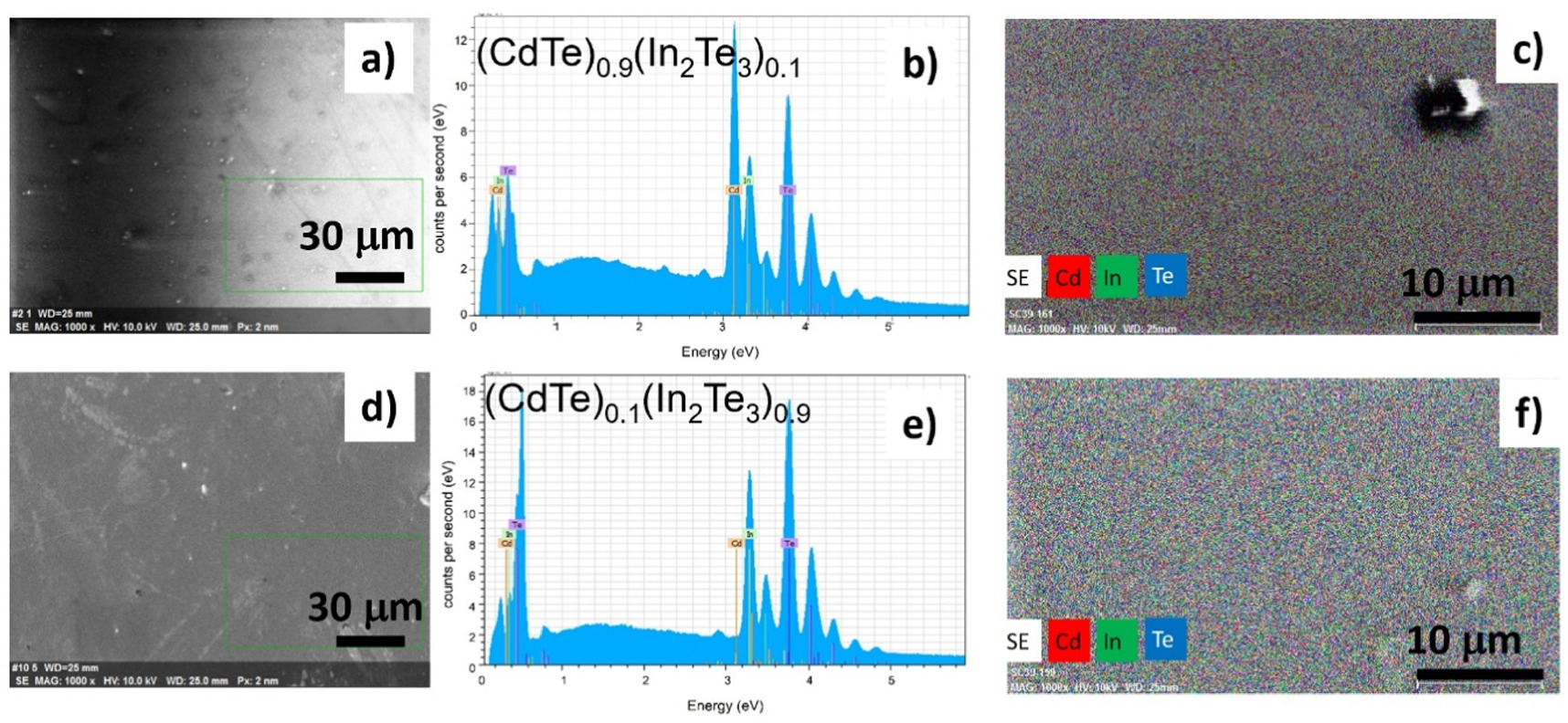
Figure 1. Scanning electron images of the surface (a), (d); energy dispersive spectra (b), (e); and elemental mappings (c) and (f) of (CdTe)0.9(In2Te3)0.1 and (CdTe)0.1(In2Te3)0.9 films, respectively. Elemental mappings showed a uniform distribution of all elements. The elemental compositions (Cd, In, Te) expressed in at% are (44, 5, 51) and ( 3, 27, 70) for x = 0.1 and x = 0.9 respectively.
Download figure:
Standard image High-resolution imageThe chemical composition of the samples was obtained by energy dispersive spectroscopy, composition values are reported in table 1 and graphically shown in figure 2. RF sputtering is a technique that preserves target composition to a good extent, but semiconductor alloys formation depends on several factors. In this case, a relevant one is the difference in sputtering yield of CdTe and In2Te3. In figure 2, the solid lines correspond to a determination of elemental composition according to the formula (CdTe)1-x(In2Te3)x without taking into account any chemical parameter such as bond strength. The experimental composition of Cd has a similar trend to that established by the formula (CdTe)1-x(In2Te3)x, suggesting a good solubility of Cd in the In2Te3 matrix. The behavior of Te and In contents suggests a stronger chemical interaction between these elements. It may be noticed that under the growth conditions used, the tellurium concentration does not get close to values corresponding to the formation of the compound CdIn2Te4.
Table 1. Parameters of (CdTe)1-x(In2Te3)x solid solution films.
| x | Cd ± 1 (at%) | In ±1 (at%) | Te±1 (at%) | a ± 0.005 (Å) | D ± 2 (nm) | Pcrystallite ± 0.5 (degree) | E0 ± 0.01 (eV) | t ± 10 (nm) | ρ (ohms cm) |
|---|---|---|---|---|---|---|---|---|---|
| 0.1 | 44 | 5 | 51 | Cubic: 6.42 | 127 | 23.9 | 1.46 | 630 | (3.1 ± .05) × 109 |
| 0.2 | 35 | 12 | 53 | Cubic: 6.38 | 119 | 24.3 | 1.48 | 660 | (1.6 ± .05) × 109 |
| 0.3 | 28 | 15 | 57 | Partially disordered | 16 | 25.5 | 1.58 | 740 | (3.4 ± .05) × 109 |
| 0.4 | 25 | 16 | 59 | Partially disordered | 14 | 25.8 | 1.55 | 740 | (2.1 ± .05) × 109 |
| 0.5 | 21 | 18 | 61 | Partially disordered | 16 | 25.8 | 1.56 | 720 | 1070 ± 5 |
| 0.6 | 17 | 18 | 65 | Partially disordered | 14 | 26.4 | 1.51 | 990 | 4.9±.05 |
| 0.7 | 15 | 15 | 70 | Partially disordered | 14 | 26.4 | 1.43 | 450 | 7.2±.05 |
| 0.8 | 6 | 23 | 71 | Partially disordered | 14 | 27.2 | 1.32 | 1330 | .4±.05 |
| 0.9 | 3 | 27 | 70 | Partially disordered | 13 | 26.9 | 1.25 | 1450 | 53 ± 1 |
| 1 | 0 | 33 | 67 | Cubic: 19.10 | 28 | 27.2 | 1.22 | 1800 | 44 ± 1 |
x: Nominal content; a: Lattice parameter; D: crystallite size; Pcrystallite : Position of peak for crystallite size calculation; E0: Bandgap; t : Thickness; ρ: Resistivity.

Figure 2. Elemental composition of the (CdTe)1-x(In2Te3)x films obtained by energy dispersive spectroscopy measurements. Solid lines correspond to the determination of the nominal compositions considering just atomic contents: (1) [Cd] = 100(1-x)/(2+3x); black line, (2) [In] = 200x/ (2+3x); red line, (3) [Te] = 100(2x+1)/(2+3x); green line.
Download figure:
Standard image High-resolution imageFigure 3 presents the x ray diffractograms of three selected samples. The whole set of diffractograms are reported in figure S1. In figure 3 the diffractograms for x = 0.1(Cd0.44In0.05Te0.51), x = 0.5(Cd0.21In0.18Te0.61), and x = 1(In0.33Te0.67) are presented. The diffractogram of the In0.33Te0.67 film (x = 1) indicates preferential growth of the (440) planes (2θ = 27.3°). X ray reflections are in close agreement with those of cubic In2Te3, some of them are indicated with open triangles in figure 3 (PDF card: 331488) [26]. The feature at 22.7 degrees corresponds to reflections of the (420) planes. In the range of 35–50 degrees, features with lower intensity are observed. For x = 0.5 (Cd0.21In0.18Te0.61), two broad peaks are observed around 25 and 44 degrees. As presented in figure S1, similar characteristics are observed in the XRD of the films with compositions between x = 0.3 (Cd0.28In0.15Te0.57) and x = 0.9 (Cd0.03In0.27Te0.70). A first approximation to explain these features is to consider that a structural amorphization of In2Te3 is induced as Cd atoms incorporated randomly in the lattice. The similarity between the patterns despite their different Cd contents could be associated to the Cd incorporation in sites of ordered vacancies in the crystalline structure of In2Te3 [11]; however, this needs further verification. It is worth mentioning that similar characteristics had been observed in the XRD of MoS2 samples due to the weak van der Waals interaction between layers [27]. For samples with x = 0.1 (Cd0.44In0.05Te0.51) and x = 0.2 (Cd0.35In0.12Te0.53), the XRD patterns do not show peaks related to the presence of In2Te3 (below the detection limit); instead, the CdTe crystalline features are dominant. In figure 3, diffractions related to cubic and hexagonal structures of CdTe are indicated by squares and hexagons, respectively [28]. For x = 0.2 (Cd0.35In0.12Te0.53), figure S1, the peaks related to the (002), (220) and (311) planes of cubic CdTe are slightly shifted towards larger angles indicating, besides the favored substitutional incorporation of In, the possible presence of stress. For larger In contents a transition to amorphous structures is observed. A solubility limit for In in crystalline CdTe could be proposed to exist between 5 and 12 percent, as inferred from the EDX and structural measurements. For the film with x = 0.1 (Cd0.44In0.05Te0.51) it is possible to identify a mixture of hexagonal and cubic phases of CdTe due to the presence of the hexagonal (100) peak near 23 degrees. The peaks around 23, 39 and 46 degrees are associated to planes (111), (220) and (311) of cubic CdTe (PDF cards: 190193 and 150770) [28]. The high crystallinity observed in the x = 0.1 (Cd0.44In0.05Te0.51), x = 0.2 (Cd0.35In0.12Te0.53) and x = 1 (In0.33Te0.67) samples demanded a detailed analysis; it was carried out employing the software WinXPOW [29]. The results obtained, reported in table 1, indicate that both samples, x = 0.1 (Cd0.44In0.05Te0.51) and x = 0.2 (Cd0.35In0.12Te0.53), have a cubic structure based in CdTe, modified by substitutional In while the fitting for sample x = 1(In0.33Te0.67) allowed identifying the cubic phase of In2Te3.
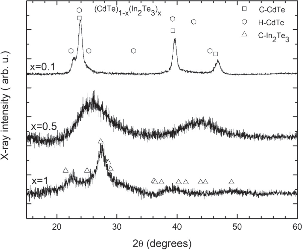
Figure 3. X-ray diffractograms of representative samples. Diffraction peaks of In2Te3 are broadened by Cd incorporation. Squares, hexagons and triangles correspond to the diffraction from planes of cubic CdTe, hexagonal CdTe and cubic In2Te3, respectively. The elemental compositions (Cd, In, Te) expressed in at% are (44, 5, 51), ( 21, 18, 61) and (0, 33, 67) for x = 0, x = 0.5 and x = 1, respectively.
Download figure:
Standard image High-resolution imageThe presence of broad x-ray reflections from planes close to those of In2Te3 from compositions x = 0.3 (Cd0.28In0.15Te0.57) and greater, with small variations (figure S1), suggests that Cd atoms incorporated substitutionally into the ordered vacancies structure of In2Te3. These results establish a solubility limit for Cd incorporation in the In2Te3 lattice at around 25 at%. Beyond 25 at% of Cd (x = 0.1, (Cd0.44In0.05Te0.51) and x = 0.2 (Cd0.35In0.12Te0.53)) In induces strain in the cubic phase of CdTe, as evidenced from the shifts in the position of the peaks. Lattice parameters and crystallite size were determined for samples with x = 0.1(Cd0.44In0.05Te0.51), x = 0.2(Cd0.35In0.12Te0.53) and x = 1(In0.33Te0.67) through the fitting process using the software WinXPOW. For the amorphous samples, sizes were determined by the Scherrer method employing FWHM of the highest intensity peak. The results of the XRD analyses are reported in table 1. It should be noted that crystallite size obtained by x-ray diffraction is smaller than the values obtained by other techniques like transmission electron microscopy, because the width of Bragg reflections is affected by micro strain, dislocations, twin planes and stacking faults.
From the XRD results it is likely that Cd atoms incorporate randomly with high probability in substitutional form in the available ordered vacant sites of In2Te3. In agreement with this, an effect on the electronic properties of the (CdTe)1-x(In2Te3)x samples should be expected. Figure 4 presents the optical transmission spectra in the range from 300 to 2500 nm of the same samples reported in figure 3. A shift in the absorption edge is clearly observed from 840 nm (x = 0.1(Cd0.44In0.05Te0.51)), 780 nm (x = 0.5(Cd0.21In0.18Te0.61)) up to 1020 nm (x = 1(In0.33Te0.67)). The complete set of transmission spectra are reported in figure S2; the shift in the position of the absorption edge as a function of composition is also clearly noticeable. The observed oscillations in the transmission spectra were due to multiple light reflections interference from the air/film and film/substrate interfaces [30]. Table 1 includes the values of the thickness for the studied samples obtained by the methodology proposed by R. Swanepoel using the optical constants of CdTe and In2Te3 [31–33].
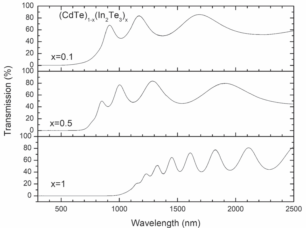
Figure 4. Optical transmission spectra of samples with different compositions. The absorption edge shifts to higher energies as the content of In2Te3 diminishes. The elemental compositions (Cd, In, Te) expressed in at% are (44, 5, 51), (21, 18, 61) and (0, 33, 67) for x = 0.1, x = 0.5 and x = 1, respectively.
Download figure:
Standard image High-resolution imageIn order to have an estimation of the samples´ bandgap, the absorption coefficient was determined employing the Beer–Lambert´s law. CdTe is a direct bandgap material and evidence exists that In2Te3 has also direct bandgap characteristics [14, 34]. The absorption coefficient of each film was analyzed by using the model of direct transitions between parabolic bands; however, further studies are necessary to validate its applicability for the whole range of compositions:

where α is the absorption coefficient, hυ the photon energy, d the film thickness, M is a constant related to the transition matrix and E0 is the bandgap energy [30]. It is worth mentioning that this work, to the best of our knowledge, is the first study of (CdTe)1-x(In2Te3)x films in the wide range of composition reported.
The bandgap was determined from the optical thickness (αd) directly from the experimental transmission spectra. Figure 5 presents the bandgap as a function of the experimental Cd concentration in the samples. The inset in figure 5 illustrates the procedure to obtain E0: the intersection between the linear fit of the absorption edge and the horizontal axis corresponds to the bandgap, according to equation (1). The same approach was applied in a systematically way to the whole set of transmission spectra. The fitting region was chosen to avoid structures due to interference features and absorption below the absorption edge due to defects [30].

Figure 5. Bandgap of the films as a function of Cd contents. The values were obtained considering the model of direct transitions between parabolic bands. The inset illustrates the methodology to obtain the value of E0 for the film (CdTe)0.5(In2Te3)0.5. The elemental composition (Cd, In, Te) expressed in at% is (21, 18, 61) for x = 0.5.
Download figure:
Standard image High-resolution imageAs observed in figure 5, as the Cd content augments the bandgap increases from that of In2Te3, reaching a maximum of 1.58 eV at Cd concentration of 28 at%. For larger Cd concentrations the bandgap decreases approaching the value of 1.5 eV, which corresponds to CdTe. There is a quasi-linear increment of E0 as Cd incorporates into In2Te3 up to Cd contents of 21 at% (x = 0.5(Cd0.21In0.18Te0.61)).
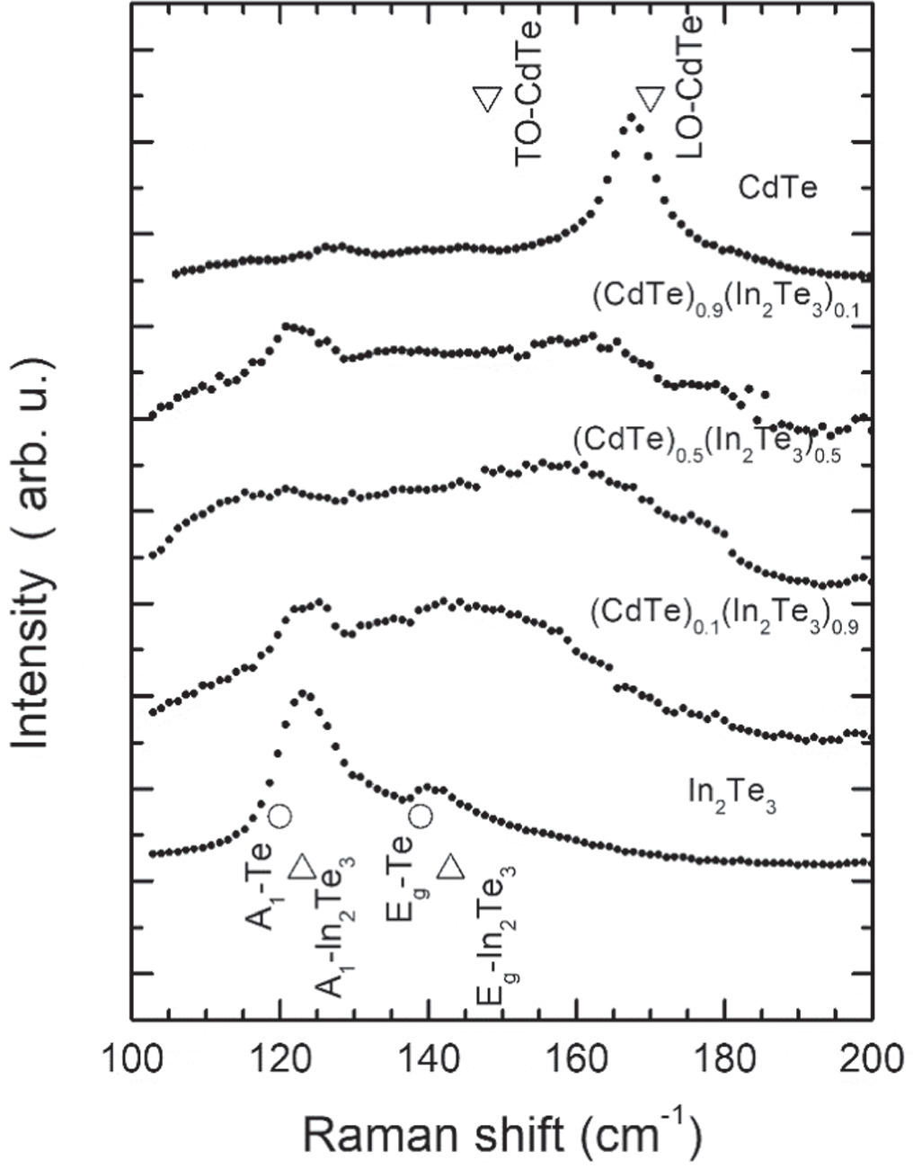
An understanding on the lattice dynamics properties of (CdTe)1-x(In2Te3)x was provided by the Raman spectroscopy characterization. Figure 6 shows the Raman spectra of CdTe, In2Te3 and of alloys with x = 0.1 (Cd0.44In0.05Te0.51), x = 0.5 (Cd0.21In0.18Te0.61) and x = 0.9 (Cd0.03In0.27Te0.70). Figure S3 presents the Raman spectra of the whole set of samples. The spectrum of CdTe shows the longitudinal optical (LO) mode at 168 cm−1 and a low intensity feature at 127 cm−1 originated from excess Te [35]. The transverse optical mode (TO) of CdTe is barely noticeable at 147 cm−1. The Raman spectrum of the In2Te3 film has two dominant bands at 123 and 140 cm−1, figure 6, in agreement with two of the most intense peaks (123 and 143 cm−1) in the Raman spectrum of high-quality In2Te3 polycrystals [36]. In general, the incorporation of Cd in the In2Te3 lattice, or the incorporation of In in the CdTe lattice, produced drastic changes in the Raman spectra of the end binary compounds, even for the smallest concentrations of In (x = 0.1(Cd0.44In0.05Te0.51)) and Cd (x = 0.9(Cd0.03In0.27Te0.70)). That is, the Raman bands of the binary compounds were broadened significantly upon the incorporation of a third element. This broadening was a common feature in the spectra of the alloys. Usually, the broadening of Raman peaks is associated to crystalline disorder or finite crystal size effects [37, 38]. In this case, the features observed in the x-ray diffractograms as the Cd atoms incorporate randomly to In2Te3 would suggest that broadening of the phonon modes is associated to incorporation of Cd in ordered vacancies sites; there is not an increase in the broadening of the XRD peaks as x augments.
Figure 6. Raman spectra of films of the end binary compounds CdTe and In2Te3, and of the (CdTe)1-x(In2Te3)x alloys with x = 0.1, 0.5, and 0.9 where a significant mode broadening is evident. Elemental compositions (Cd, In, Te) expressed in at% are (44, 5, 51), ( 21, 18, 61) and (3, 27, 70) for x = 0.1, x = 0.5 and x = 0.9, respectively. Open symbols correspond to Raman modes of: Te (open circles), In2Te3 (open triangles) and CdTe (open inverted triangles).
Download figure:
Standard image High-resolution image
It has been reported that the presence of ordered vacancies may reduce the number of Raman active vibrational modes [36]. It is expected that the similar atomic masses of Cd and In would produce small shifts in the energy of phonons, and because of the structural disorder, the optical-phonons lifetime would decrease, as reflected by the broad peaks.
A special mention is necessary for the film with x = 0.1 (Cd0.44In0.05Te0.51) since it presents well defined XRD peaks, with significantly broad Raman features. A possible source for the observed broadening may be the random incorporation of In atoms in Cd-vacancy sites of CdTe and the concurrent mass and force constant fluctuations. Indeed, recent studies on phonon broadening in high entropy alloys [39, 40] showed that these types of fluctuations may produce important phonon broadening. Additionally, the XRD data showed that the In incorporation produced strain (compression) in the CdTe lattice since there is a shift to larger angles of the main diffraction peak of the x = 0.2 (Cd0.35In0.12Te0.53) film, with respect to the equivalent peak of the x = 0.1 (Cd0.44In0.05Te0.51) film, figure S2. That is, these two combined effects may be the origin of the phonon broadening: mass and force constant fluctuations and inhomogeneous strain. Further work is necessary to gain better understanding on this matter.
In crystalline bulk materials heat conduction is associated to acoustic phonons. An increase in phonon scattering may decrease thermal conductivity [41]. It has been reported that changes in the chemical environment of atoms in the crystalline structure of vacancy ordered materials produce strong anharmonicity of vibrational states decreasing their thermal conductivity [42]. The increase in the width of Raman peaks (i.e. lifetime reduction) may be associated to the incorporation of Cd in ordered vacancy positions in In2Te3, increasing phonon scattering and, consequently, the thermal conductivity of (CdTe)1-x(In2Te3)x would decrease. It may be hypothesized that the change in phonon width observed in the Raman spectra along with the crystallinity characteristics observed in the x-ray diffractograms would suggest that (CdTe)1-x(In2Te3)x may have potential as thermoelectric material, especially for the compositions with low resistivity.
The resistivity of the samples with Cd content above 20 at% (nominal x = 0.5 (Cd0.21In0.18Te0.61)) have values of the order of 109 ohm-cm. On the other hand, for low Cd concentrations the resistivity decreases. For x = 0.8 ((Cd0.06In0.23Te0.71)) the lowest value of resistivity was obtained (0.42 ohm-cm). The resistivity of the films is reported in table 1 and presented in figure S4. The decrease in resistivity due to the incorporation of low percentages of Cd has been reported in bulk InTe [43].
Conclusions
The structural characterization and study of the electronic properties of (CdTe)1-x(In2Te3)x films produced by RF sputtering show a successful bandgap tuning depending on the Cd concentration. X-ray diffraction results indicate the presence of partially crystalline phases which were associated to the incorporation of Cd into the In2Te3 crystal structure for 0.3 ≤ x ≤ 0.9. The XRD data suggest that a possible substitutional incorporation of In in the CdTe lattice up to a nominal composition of x = 0.3 may be achieved, which corresponds to In concentrations between 5 and 12 at% as obtained by EDX. Considering the other limit of the solid solution (In2Te3), the random incorporation of Cd in the ordered-vacancy sites of In2Te3 produced poor crystalline characteristics that remained for Cd concentrations between 2 and 28 at%. The bandgap reached a maximum of 1.58 eV at Cd contents of 28 at%. At low Cd concentrations the resistivity of the (CdTe)1-x(In2Te3)x films decreased until reaching a minimum for 6 at%, while for Cd contents larger than 20 at% the resistivity increased nine orders of magnitude. For both end binary compounds the random incorporation of a third chemical element produced a significant broadening of the Raman modes, consistent with a reduction in the lifetime of the optical phonons.
The bandgap variation indicates that (CdTe)1-x(In2Te3)x films could find potential applications in photovoltaics. While partial amorphization could affect thermal lattice properties, an increase in conductivity would made worth studying the thermoelectric properties of (CdTe)1-x(In2Te3)x films for some In2Te3 compositions.
Acknowledgments
We acknowledge the technical support of Angel Guillen and Marcela Guerrero from the Physics Department at Cinvestav-Zacatenco and the technical support of Abraham Israel Calderón-Martínez from Cinvestav-Queretaro, and the partial financial support from CONAHCYT-Mexico.
Data availability statement
All data that support the findings of this study are included within the article (and any supplementary files).
Availability of data and materials
All the data are available upon request.
Competing interests
The authors declare that they have no known competing financial interests or personal relationships that could have appeared to influence the work reported in this paper.
Supplementary data (1 MB DOCX)