

Abstract
This work investigates optoelectronic properties of SiC- and GeC-hybrids that are still unexplored. Using DFT and many body effect calculations, we study, among others, charge density, dielectric functions, reflectivity and electron energy loss spectroscopy. The charge transfer determines the bonds nature between the atoms constituting the hybrids. A comparative study of gap and binding energy using different approximations is presented. The dielectric functions reveal strong excitonic effects. Two peaks related to p and p+s electron plasmons are observed in the spectra of loss energy. Moreover, the analysis of reflectivity shows that hybrids are transparent in the visible region. Other interesting findings are also detailed.
Export citation and abstract BibTeX RIS
1. Introduction
During the last decade, graphene has attracted a big deal of interest owing to its outstanding structural and electronic properties and promising applications in nanotechnology [1, 2]. Graphene is characterized with an absorption of 2.3% in the white light spectrum [3] and an excellent optical transmittance (97%) in the visible light range [3]. It is also the strongest material ever discovered with its high elastic modulus (1.02 TPa) and intrinsic strength (130 GPa) [4]. Moreover, a high thermal conductivity of 5000 W mK−1 [5], a huge charge carrier mobility at room temperature of 15.000 cm2 V−1 s−1 and a large specific surface area of 2630 m2 g−1 [6] were measured for this revolutionary material.
The intensive studies on graphene have led to further research in exploring other two-dimensional (2D) systems [7]. Silicene and germanene are two graphene counterparts that are energetically favorable as low buckled honeycomb structures [8]. These two materials inherit of some of the exceptional properties of graphene such as the zero-gap with bands crossing linearly at the Fermi level [9]. Although silicene and germanene do not exist in nature in free-standing form, they were successfully synthesized on different substrates, namely on Ag(111), Ir(111) and ZrB2 surfaces for silicene [10–12], and on Al(111) and Au(111) substrates in the case of germanene [13, 14].
The absence of a band-gap in the energy spectrum of this set of 2D materials presents a serious hurdle for their applications in electronic [8, 9]. One way to overcome the problem is to combine between atoms to generate graphene compounds namely silicene/graphene (SiC) and germanene/graphene (GeC) hybrids. In these new materials, the hybridization between X and C atoms (X = Si or Ge) is sp2 at the expense of sp3 hybridization that is preferred by silicon and germanium [15, 16]. Therefore, the hybrids shows a perfectly planar honeycomb structures where carbon atoms bind X-atoms in an alternating arrangement. The asymmetry in the hexagonal lattices opens the gaps in the hybrids.
In SiC, excitonic effects are as significant as in silicene and graphene with a large binding energy of 0.81 eV using GW that uses a LDA starting point [17]. GeC system exhibits stronger excitonic effects for light polarization along and perpendicular to its plane. A large binding energy of 1.82 eV is obtained for the first exciton using GGA [18]. The first active excitons exhibit large Bohr radius of 2.78 Å and 2 Å in SiC and GeC respectively. These first results on optical properties show how these materials could be promising candidates for optoelectronic applications.
Interestingly, chemical modification of these two sheets using radicals was investigated to control their gap energy, induce magnetism or enhance their optical and mechanical properties. Adsorbed hydrogen atoms in SiC structures characterized by different stoichiometry were investigated as promising candidates for hydrogen storage using molecular dynamic simulation strategy [19] and DFT-GGA approach [20]. Tuning the binary compounds of Group-IV elements by chemical species and hydrogen adsorption gives rise to ferromagnetic/antiferromagnetic coupling and different band gap characters [21, 22]. Decorations with F-atoms, that have high Pauling electronegativity, are exothermic adsorptions in both GeC and SiC which indicates the possibility of realizing them in experiments [23, 24]. A net magnetic moment is observed in SiC sheet upon creating a single Si-vacancy while the other vacancy defects, such as C-vacancy and Si+C divacancy, are found to influence electronic properties without attaining any magnetic order [25]. In GeC sheet, the adsorption of C, Si and Ge atoms induces n- and p-type doping and modulates the intrinsic characteristics of the resulting derivatives [26].
In the present work, first-principles density functional calculations are performed to seek more the electronic and optical properties of both GeC and SiC that are still not explored. Charge transfer analysis inform us about the type of interatomic bonds. Imaginary and real part of dielectric function as well as electron energy loss spectroscopy are given and discussed. Reflectivity spectra shows that the SiC is more transparent than GeC in the visible region. The big gap energy of SiC reduces its refraction index compared to GeC. Two peaks related to π and  electron plasmons are observed in the spectra of the loss energy in the two hybrids. The analysis of the imaginary part of the dielectric functions reveal strong excitonic effects. Along all this work, a comparative study between the two hybrids is presented.
In this paper, we start by detailing computational method that we use then we report and discuss the obtained results in section 3. We end with a conclusion.
2. Computational details
The numerical calculations are provided by Quantum Esspresso code [27] where Kohn–Sham equations are solved self-consistently [28] . Electronic wave-functions are described using projector augmented wave potentials. The generalized gradient approximation (GGA) of Perdew–Zunger (PZ) exchange-correlation functional [29] is used for a plane-wave basis set with kinetic-energy cutoff of 60 Ry. In the self-consistent potential and total-energy calculations, the Brillouin zone (BZ) is sampled by special k-points with a number of 20 × 20 × 1. A vacuum region of 20 Å is introduced to eliminate any artificial interaction between neighboring supercells along the perpendicular direction. Charge transfer is obtain through Bader analysis. To perform QP calculations within many-body perturbation theory, we replace the exchange-correlation potential Vxc used in the DFT by a non-local, energy-dependent self-energy operator  defined as [30]:

where r1 and r2 denote electron hole and position. These non-self consistent GW calculations are performed using YAMBO program suite [31]. A 12 × 12 × 1 k-points mesh is used for the calculations of QP energies, while a 24 × 24 × 1 k-point mesh is used to evaluate dielectric function in Bethe–Salpeter equation (BSE) [30]
3. Results and discussion
3.1. Charge transfer
Both SiC and GeC sheets are stable in planar hexagonal lattices [1, 2] with all their bond angles equal to 120°. The interatomic bond lengths dGe−C = 1.89 Å and dSi−C = 1.78 Å for GeC and SiC respectively are nearly 30% smaller than their bulk materials.
The calculated charge transfer between atoms shows that each Ge atom gives about 0.48e to one of its C-atom neighbor. This indicates a covalent-ionic bonding between C and Ge atoms in GeC hybrid. Meanwhile, the picture is a little bit different in SiC sheet where a huge amount of 1.38 electrons is pulled away from Si- to each C-atoms making the bonding between them ionic. Notice that charge transfer between atoms can be attributed to the Pauling electronegativities χ of C(2.55), Ge(2.01) and Si (1.9), since electrons transfer from atoms with lower χ towards those with higher electronegativity.
To shed more light on charge transfer and give more information about interactions between the involved atoms, figure 1 plots charge density distribution around each atom of SiC and GeC systems. One can see that charge distribution around carbon atoms is more important compared to Si or Ge-atoms. This fact is mainly due to highest electronegativity of carbon. Moreover, the significant charge density overlap between Ge and C atoms in GeC, that is shown in figure 1, confirms the covalent-ionic bonding in this material. However, the negligible charge overlap in SiC system clearly reveals that the bonding between Si and C atom is effectively ionic in good agreement with the reported Bader charge analysis.
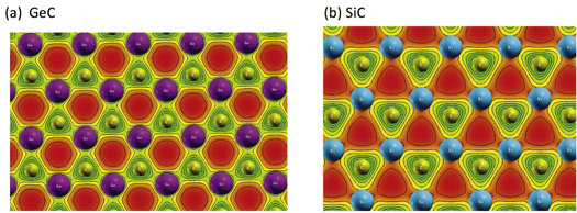
Figure 1. Charge density distribution for (a) GeC and (b) SiC
Download figure:
Standard image High-resolution image3.2. Electronic structure
Figure 2 shows the gap energy obtained by using two different approximations, namely GW and GGA. The band gap is higher in SiC compared to GeC. The difference is about 19% and only 1.9% in favor of GeC using GGA and GW techniques [1, 2]. Noting that GGA underestimates the gap energy while GW is known to give more accurate values that are comparable with experiments. The smaller gap in GeC with respect to SiC can be attributed to the fact that Ge-atom is bigger than Si-one in good agreement with the work on SnC [16]. This decreasing in energy gap between SiC and GeC can also be explained in terms of the conduction level splitting. Indeed, the π-like antibonding states in the lowest conduction level of heavier systems tends to move down relative to the π-like states at the maximum valence band, leading to a decreasing of the gap.
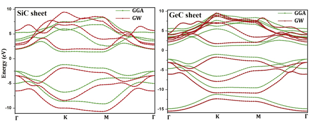
Figure 2. Band structure of SiC and GeC monolayers. The red and green curves represent the bands obtained using GW and GGA approximations respectively.
Download figure:
Standard image High-resolution imageTo understand the contribution of atoms in the gap energy Eg of GeC and SiC, we examine charge density in the lowest conduction band (CBM) and the highest valence band (VBM) as well as the partial density of states plotted in figures 3 and 4. In GeC, CBM is totaly composed by Ge-atoms while C-atoms contribute mainly to VBM. In SiC, VBM originates from C-atoms while Si atoms form CBM. It follows that in both GeC and SiC systems, C-atoms dominate the VBM and have trifling contribution in the CBM.
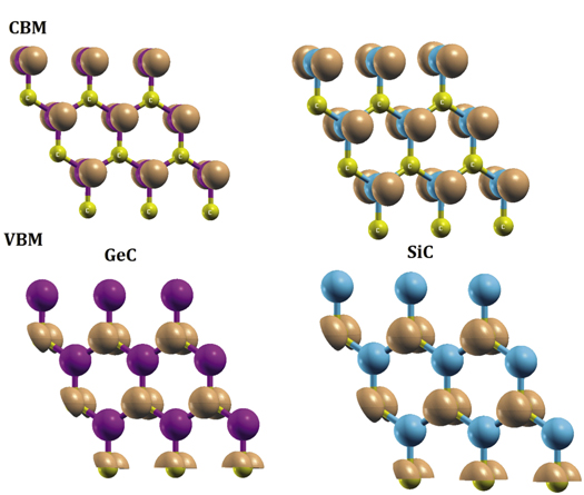
Figure 3. Charge density associated to the lowest conduction band (CBM) and the highest valence band (VBM) of GeC and SiC. The isovalue is set at 0.015 e Å−3
Download figure:
Standard image High-resolution image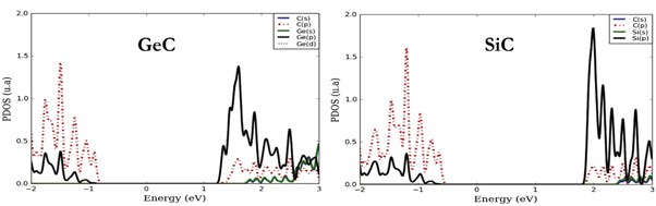
Figure 4. Projected density of states (PDOS) corresponding to GeC and SiC
Download figure:
Standard image High-resolution imageThe first analysis of electronic projected density of states around the Fermi level shows that in GeC the states in valence (conduction) band originate from p-orbitals of C-atoms (Ge-atoms) in perfect consistence with the previous result. In SiC, the main contribution in conduction band and valence band results from p-electrons of C-atoms and Si-atoms respectively.
3.3. Optical properties
The imaginary part of the dielectric function  is very crucial to determine the optical absorption spectra. Figure 5 presents this function for GeC and SiC hybrids by including electron–hole interactions and using the Bethe–Salpeter equation (GW+BSE). Only the absorption spectra for the incident light polarized along the x-axis (that coincides with zigzag-direction) is considered. The first peaks are observed in the absorption curves at 2.48 eV and 1.62 eV for GeC and SiC respectively using BSE built from GGA in good agreement with previous works [17, 18]. At Γ-point of the BZ, these strong bound excitons result from the vertical transitions between the top of the valence band (degenerated) and the bottom of the conduction band. Their binding energy are reported in table 1 using BSE+GW calculations based on GGA approximation. Binding energy is higher in GeC compared to SiC. It follows that the e–h interactions are strong in SiC and much stronger in GeC due to quantum confinement.

Figure 5. BSE plot of imaginary and real parts of dielectric functioncorresponding to SiC and GeC hybrids.
Download figure:
Standard image High-resolution imageTable 1. Gap energies Eg and binding energy Eb in eV, static dielectric and static refraction associated to GeC and SiC hybrids.

|

|
Eb |

|
n0 | |
|---|---|---|---|---|---|
| SiC | 2.52 | 3.53 | 1.05 | 2.06 | 1.43 |
| GeC | 2.05 | 3.45 | 1.81 | 3.56 | 1.88 |
Using BSE-GW, figure 5 displays also the real parts of dielectric functions describing SiC and GeC systems. This parameter give information about the electronic polarizability of the material through the Clausius–Mossotti relation. The real parts of dielectric functions takes negative values in the intervals [1.66–1.82], [2.39–2.48], [6.00–6.87] and [7.65–7.83] eV for GeC monolayer, and in the ranges [2.50–2.73], [2.95–3.70], [6.50–7.29] and [7.94–9.91] eV in SiC hybrid. This result indicates the metallic character of SiC and GeC in these intervals of the electromagnetic spectrum.
Based on macroscopic dielectric functions, one can derive linear optical quantities as well as the electron-energy-loss function.
As reported in table 1, the static dielectric function  is 3.56 in GeC higher than 2.06 obtained for SiC showing that GeC have relatively high polarizability compared to SiC. This corresponds to the values of refraction index at zero energy. In Penn's model, the index
  is inversely proportional to the energy of direct band gap and it is expressed as follows [32]:

where ωp and Eg are the plasma frequency and the energy band gap, respectively. One can see that this inverse feature provides lower value of  to SiC that has larger gap energy. The complex refraction index is given by

where n and k are the refraction and the extinction indexes respectively. They are calculated using the following expressions:
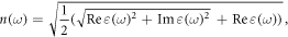
The two top plots in figure 6 show that in both GeC and SiC, the refraction index is minimum where absorption is maximum and the extinction index is higher around the plasma frequency. The maximum of the refraction index emerges at 2.44 and 1.53 eV while the maximum of the extinction index is observed at 2.52 and 1.66 eV for SiC and GeC respectively. At these energies the photons will be absorbed very fast as the extinction index indicates the amount of absorption loss when the electromagnetic wave propagates through the material.
Figure 6. Optical properties of SiC and GeC sheets: refraction index (a) extinction index (b) energy loss function (c) reflectivity (d) including excitonic effects.
Download figure:
Standard image High-resolution image
At normal incidence, the Fresnel reflectivity of solids R(ω ) is given by:

with  is the complex dielectric function. It is evident when examining figure 6(c), that SiC and GeC compounds are semiconductors since their reflectivity R(ω ) values do not approach the unity towards zero energy. The reflectivity spectra shows a zero frequency reflectivity R(0) of 9.3% for GeC and much smaller (0.26%) for SiC. However, the maximum value of 57.3% is observed in the visible region near the UV for SiC and 54.6% emerges at the UV region for GeC. According to figure 6(c), more reflectivity arises in ultraviolet region. Consequently, SiC and GeC can be used as transparent materials in optoelectronic industry in the 0−2 eV area and above 10 eV respectively.
The energy-loss function L(ω ), is another important parameter, that is describes the energy loss of a fast electron traversing a material. It is deduced from the following equation:
Similar to graphene, the energy-loss spectrum displays two main peaks related to π and  electron plasmons, respectively (see figure 6(d)). In SiC, these peaks are located around 3−5 eV and 9−11 eV while they are observed around 2−3 and 7−9 eV in GeC. Furthermore, between these two peaks appear some weak peaks which indicate weak resonances. Finally, by comparing figures 5 and 6, one can deduces that the peaks in energy loss function results from the change in the sign of the real dielectric function.
4. Conclusion
In summary, optoelectronic properties of both SiC and GeC nanosheets are studied using DFT and GW+BSE. Bader charge density analysis provides ionic and covalent-ionic bonding nature for SiC and GeC respectively. Moreover while C-atoms contribute mainly in the VBM, the two lowest conduction bands originate mainly from Si and Ge atoms. Using different techniques of calculations, it is found, among others that, both the band gap energy and the binding energy of the first bright exciton in GeC are higher compared to that of SiC. The static dielectric of GeC is also higher than that one of SiC, which indicates that GeC has high polarizability compared to SiC. The maximum of extinction index emerges at 2.52 and 1.66 eV for SiC and GeC, respectively. At these energies, the photons depth paths will be the shortest. The energy-loss spectra display two main peaks related to π and  electron plasmons, respectively.
Acknowledgments
The authors would like to acknowledge financial support from the Centre National pour la Recherche Scientifique et Technique (CNRST)-Morocco.