

Abstract
In this paper, we report a facile growth of freestanding PbI2−xClx film and microbulk via hydrothermal method without additives. The properties of samples were systematically investigated by field emission scanning electron microscopy, x-ray diffraction and UV–vis diffuse reflection spectroscopy. The results reveal that there appears to be two types of morphological PbI2−xClx due to the anisotropy in the effective surface energy, and the underlying growth mechanism behind the observation is also discussed. This new approach is promising for the fabrication of PbI2−xClx precursor material of detectors and solar cells.
Export citation and abstract BibTeX RIS
1. Introduction
Room-temperature radiation detection is widely applied in a number of areas such as industrial non-destructive tests, medical imaging, public security, etc [1, 2]. According to the important selected criteria [1], many semiconductor materials (CdZnTe, TlBr, PbI2 etc) have been investigated for radiation detection. Compared to the high processing temperature of CdZnTe (about 600 °C) and the toxicity of TlBr, PbI2 is a less toxic radiation detection material which has a lower melting point (about 406 °C) and no destructive phase transition [2, 3]. Moreover, PbI2 was also applied in the fields of solar cells, optoelectronic devices [4–7]. However, the tunable band gap of PbI2 by doping other elements such as Gd, Cl or Br was rarely reported and still remains a great challenge [8, 9].
Very recently, many reports showed that PbI2−xClx is an excellent and burgeoning precursor material of perovskite solar cells [10–12]. Wu et al [10] first fabricated the PbICl thin film with low crystallinity and porous morphology via a vapor-assisted solution process, it can be easily converted to planar perovskite solar cells without lead halide residuals, and the highest photovoltaic conversion efficiency (PCE) can achieve 11.11%. Luo et al [11] have investigated the influence of chloride for perovskite solar cells by the interdiffusion method, and found that particles were formed at a low PbCl2 ratio while the PbICl phase was formed at a high PbCl2 ratio. However, the aforementioned fabrication methods are complicated, and the organic reagent such as N, N-dimethylformamide (DMF) applied in these reports, adds an extra cost.
In this work, the freestanding PbI2−xClx film and microbulk were fabricated via a facile hydrothermal method, and the growth mechanisms of these two PbI2−xClx morphologies were also analyzed. Additionally, the PbI2−xClx film and microbulk were respectively characterized by ultraviolet–visible diffuse reflection spectroscopy (UV–vis DRS), x-ray diffraction (XRD) and field emission scanning electron microscopy (FE-SEM), respectively.
2. Experimental method
All chemicals were commercially available and used without further purification. In a traditional procedure, the total molar quantity was fixed at 0.25 m mol. 0.0070 g (0.025 m mol), 0.0139 g (0.05 m mol), 0.0209 g (0.075 m mol), 0.0278 g (0.1 m mol), 0.0348 g (0.125 m mol) PbCl2 powder (Aldrich Chemistry Reagent) was respectively added into 15 ml of deionized water with corresponding 0.1037 g (0.225 m mol), 0.0922 g (0.2 m mol), 0.0807 g (0.175 m mol),0.0692 g (0.15 m mol), 0.0576 g (0.125 m mol) PbI2 powder(Aldrich Chemistry Reagent). The xPbCl2:(1 − x)PbI2 (molar ratio, x = 0.1, 0.2, 0.3, 0.4 and 0.5) powder was placed into a 30 ml Teflon-lined autoclave, respectively. Besides that, the solubility of PbCl2 and PbI2 is 0.162 g and 0.0114 g per 15 ml H2O at room temperature [13]. They were not negligible and added into each solution as extra compensation. The autoclave was kept at 200 °Cfor 6 h and then naturally cooled to room temperature; samples were taken out of the solution from the autoclave. After naturally air drying, freestanding PbI2−xClx film and microbulk were obtained. For convenience, 0.1PbCl2 + 0.9PbI2, 0.2PbCl2 + 0.8PbI2, 0.3PbCl2 + 0.7PbI2, 0.4PbCl2 + 0.6PbI2, 0.5PbCl2 + 0.5PbI2 were respectively referred to as A (0.1:0.9), B (0.2:0.8), C (0.3:0.7), D (0.4:0.6), E (0.5:0.5).
The UV–vis DRS of freestanding PbI2−xClx film and microbulk was measured via a SHIMADZU UV-2550 UV–visible spectrophotometer (300–800 nm). The XRD data was obtained using a DX-2700 Cu Kα radiation λ = 1.543 Å (30 kV, 20mA), the scanning scope was between 10° and 80° with a step of 0.03°. The morphology of samples surface was recorded using a field-emission electron microscope (SU8020, Hitachi, Japan).
3. Results and discussion
Figure 1 shows the optical images of freestanding PbI2−xClx film and microbulk with different PbCl2/PbI2 molar ratios. Figure 1(a) presents sample A (0.1:0.9) and figure 1(b) shows sample B (0.2:0.8), the results reveal that film and microbulk coexist and cannot be fully separated out manually. Figures 1(c) and (d) respectively exhibit sample C (0.3:0.7) film and microbulk, one can see that film and microbulk still coexist but can be easily separated out by hand. Figure 1(e) shows sample D (0.4:0.6) and figure 1(f) represents sample E (0.5:0.5), in these two samples, only microbulk can be observed.
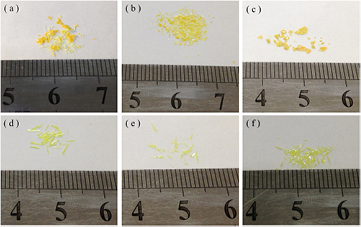
Figure 1. Optical images of freestanding PbI2−xClx film and microbulk. (a) A (0.1:0.9), (b) B (0.2:0.8), (c) C (0.3:0.7, film), (d) C (0.3:0.7, microbulk), (e) D (0.4:0.6, microbulk), (f) E (0.5:0.5, microbulk).
Download figure:
Standard image High-resolution imageFigure 2 displays the surface morphology of freestanding PbI2−xClx film and microbulk SEM images. Figures 2(a) and (b) respectively present sample A (0.1:0.9) film and microbulk, figures 2(c) and (d) respectively show sample C (0.3:0.7) film and microbulk, figure 2(e) represents sample D (0.4:0.6) microbulk, figure 2(f) exhibits sample E (0.5:0.5) microbulk. One can see that the film and microbulks coexist in figures 2(a)–(d) when the PbCl2:PbI2 molar ratio reaches 0.3:0.7 or below, with the increase of Cl content, the morphology of PbI2−xClx all turns to be microbulk.

Figure 2. SEM images of freestanding PbI2−xClx film and microbulk. (a) A (0.1:0.9, film), (b) A (0.1:0.9, microbulk), (c) C (0.3:0.7, film), (d) C (0.3:0.7, microbulk), (e) D (0.4:0.6, microbulk), (f) E (0.5:0.5, microbulk).
Download figure:
Standard image High-resolution imageFrom the observations of microstructures of PbI2−xClx film and microbulk, the growth mechanism can be worked out as follows:
As the temperature cools down, it is possible two types of crystal nucleus appear due to supersaturation and structure fluctuation in the solution, one type of crystal nucleus contains high Cl content, in contrast, the other contains less Cl content. When the temperature decreases further, the crystal nucleus with high Cl content gradually grows to be microbulk due to self-limitation of crystal structure and the anisotropy in the effective surface energy. And the crystal nucleus with less Cl content and its adherent crystal nuclei gradually grow together due to high surface energy, eventually turning to be a film via intergrowth mechanism. Moreover, when PbCl2:PbI2 molar ratio reaches to 0.4:0.6 or above, the intergrowth mechanism will find it very difficult to advance, only microbulk can exclusively proceed.
The XRD patterns of powder freestanding PbI2−xClx film and microbulk is shown in figure 3. A (0.1:0.9), B (0.2:0.8), C (0.3:0.7), D (0.4:0.6), E (0.5:0.5) was tested respectively. Note that the result agrees with the diffraction peaks in the PbICl PDF cards (JCPDS file No. PDF#73-0361), and it is in agreement with [10–12]. Besides that, it can be observed extra PbI2 diffraction peaks appeared in patterns (a)–(c), located at 2θ = 12.67°, corresponding to the reflection planes of (0 0 6) (JCPDS file No. PDF#73-1754), this phase was also observed in [10–12, 14]. The results demonstrate that the PbI2−xClx film and microbulk close to PbICl phase but with different lattice constant due to different Cl content, while the PbICl belongs to Pnam space group [15].

where α is absorption coefficient, h is Planck's constant, ν is the frequency of incident photon, A is a constant and Eg is the band gap value. When calculating Eg via a Tauc plot, the result is not influential to the Eg whether using α or absorbance (Abs), it just leads to a different constant A. So, Abs was used to replace α for convenience.
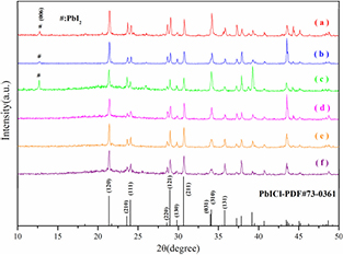
Figure 3. XRD patterns of power freestanding PbI2−xClx film and microbulk. (a) A (0.1:0.9), (b) B (0.2:0.8), (c) C (0.3:0.7, film), (d) C (0.3:0.7, microbulk), (e) D (0.4:0.6, microbulk), (f) E (0.5:0.5, microbulk).
Download figure:
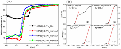
Standard image High-resolution imageFigure 4 displays the UV–vis DRS and optical band gap (Eg) plots of C (0.3:0.7), D (0.4:0.6), E (0.5:0.5). The band gap value of film and microbulk as shown in figure 4(b) were obtained from the Tauc plot equation (1) of a direct band gap semiconductor [16, 17]
Figure 4. (a) Diffuse reflectance spectra and (b) optical band gap plots.
Download figure:
Standard image High-resolution image
According to the diffuse reflection spectra, Abs can be easily obtained via the conversion equation (2)

Eg was calculated through extrapolating the linear portion of the (Abs hν)2 versus hν plot, as shown in figure 4(b). The corresponding band gap value is respectively found to be 2.34 eV, 2.63 eV, 2.70 eV, 2.65 eV of C (0.3:0.7) film, C (0.3:0.7) microbulk, D (0.4:0.6) microbulk, E (0.5:0.5) microbulk respectively. The variation trend of Eg value was similarly liked in [9, 10], here one possible reason can be giving as follows:
According to figure 4(b) (1) and (2), the Eg value of C (0.3:0.7) microbulk with high Cl content is larger than C (0.3:0.7) film with less Cl content, and this result coincides with the aforementioned SEM morphology and growth mechanism analysis, from figure 4(b) (2)–(4), the Eg value of microbulk increases initially and decreases afterwards due to the different Cl content ratio, the variety of Cl content ratio leads to the diverse lattice constant [15], and the relation between Eg value and Cl content ratio maybe is not linear, and further theoretical work is needed in the future.
4. Conclusion
The freestanding PbI2−xClx film and microbulk were fabricated in a facile hydrothermal method without any additive and characterized with SEM, XRD and UV–vis DRS. SEM images suggest that the film and microbulk morphology appears because of the anisotropy in the effective surface energy, and the underlying growth mechanisms of these two PbI2−xClx morphologies were also analyzed. Besides, the XRD demonstrates that the PbI2−xClx film and microbulk close to PbICl phase but with different lattice constant due to different Cl content. UV–vis DRS suggests that Eg of C (0.3:0.7, film), C (0.3:0.7, microbulk), D (0.4:0.6, microbulk) and E (0.5:0.5, microbulk) is 2.34 eV, 2.63 eV, 2.70 eV, 2.65 eV, respectively. This new synthesized approach of freestanding PbI2−xClx film and microbulk is maybe of great potential for use in perovskite cells and detectors.
Acknowledgments
This work was supported by the National Natural Science Foundation of China (grant no. 11675029), Technology Support Program Fund of Science and Technology Department of Sichuan Province (grant no.2014GZ0020, 2014GZX0012, 15ZB0173, 2015GZ0194 and 2016FZ0018), Sichuan Province Practice and Innovation Training Program for College Students (grant no. 201610621087), Scientific Research Fund of Sichuan Provincial Education Department No.17ZA0068, and Project (KYTZ201621) supported by the Scientific Research Foundation of CUIT.