
Abstract
In this study the influence of the spatial distribution and of different nanostructures of WO3 and Fe2O3 in the dual absorber system Fe2O3/WO3 was systematically investigated for the first time. WO3 was applied as a scaffold and/or as a surface treatment to mesoporous Fe2O3 films. Both approaches strongly increased the performance compared to the individual photoabsorbers. By combining a host guest architecture with a surface treatment, current densities of about 0.7 mA cm−2 at 1.23 V versus reversible hydrogen electrode under AM 1.5 illumination with an incident photon-to-current efficiency of 17% at 350 nm were achieved without the use of further catalysts. We could identify several beneficial interactions between Fe2O3 and WO3. WO3 strongly scatters visible light, resulting in increased absorption by Fe2O3 and higher current densities. We also determined a cathodic shift in the onset potential to 0.8 V and increased transfer rates of up to 88%. This combination of beneficial effects proves the viability of the presented device architecture.
Export citation and abstract BibTeX RIS

Original content from this work may be used under the terms of the Creative Commons Attribution 3.0 licence. Any further distribution of this work must maintain attribution to the author(s) and the title of the work, journal citation and DOI.
1. Introduction
Driven by climate change, rapid population growth and dwindling resources, research into alternative, sustainable energies is thriving. Solar cells and wind turbines, which harness the power of the sun, already play a major role in the energy mix of some countries, with their market share expected to increase. However, storage of the generated electricity is a challenge. One of many possible solutions is photoelectrochemical water splitting, which uses sun light as an energy source to generate oxygen and hydrogen from water. While suitable photoelectrode materials have been studied since 1972 [1], research has intensified in the last few years and several photocathode and photoanode materials (such as TiO2, Si or Cu2O and Fe2O3, WO3 or BiVO4, respectively) have been investigated [2–4]. Efficient photoanodes, in particular, are difficult to realize. Producing one oxygen molecule requires four holes, making recombination likely and requiring significant optimization of factors such as composition, electronic structure and morphology. All efforts notwithstanding, it is becoming more and more obvious that limitations intrinsic to many single absorber materials investigated so far, such as large band gaps, slow surface kinetics or fast bulk electron–hole recombination, are difficult to overcome. One approach towards solving this problem is the combination of different photoabsorber materials. Such a combination can increase the efficiency in several ways such as by optical absorption enhancement, enhanced charge separation, faster surface kinetics, or the modification of the electronic structure of the interface between both materials [5]. For photoanodes, a dual absorber approach has been successful for several systems such as WO3/TiO2 [6], WO3/BiVO4 [7], TiO2/Fe2O3 [8] and Fe2O3/WO3 [5, 9, 10].
The Fe2O3/WO3 system is a good model and a promising photoanode for many reasons. The individual materials are abundant and therefore cheap, non-toxic and corrosion-resistant [11, 12]. Consequently, both materials have been intensively studied, and the influence of different morphologies, dopants, surface modifications etc for both systems is well-investigated [11, 13]. WO3 has a band gap of 2.5–2.8 eV and absorbs mostly in the blue and UV spectral range [12, 14, 15]. Because of good charge transport properties and fast surface kinetics, it has proven itself a suitable candidate for water photoelectrolysis [15]. However, the large band gap limits the overall theoretical solar-to-hydrogen efficiency to 8% [16]. Fe2O3, on the other hand, has a band gap between 1.9 and 2.2 eV and also absorbs a large fraction of visible light, driving the potential solar-to-hydrogen efficiency up to 16.8% [11, 16]. Unfortunately, the expected efficiency is greatly reduced by several loss mechanisms such as high bulk and surface recombination rates and slow kinetics for the oxygen evolution reaction. Combining Fe2O3 and WO3 can improve the performance of the individual materials in several ways. Compared to bare WO3, a larger spectral range is absorbed. The band alignment of Fe2O3 and WO3 allows for the injection of electrons from Fe2O3 into WO3, with the latter being a better electron conductor. Holes, on the other hand, are injected from WO3 into Fe2O3 [17]. Sivula et al found the deposition of Fe2O3 onto WO3 scaffolds to drastically improve electron charge collection [9]. Furthermore, the rate of the oxygen evolution reaction of Fe2O3 was shown to be significantly improved by surface treatment of Fe2O3 by a WO3 layer [5, 18].
In addition to the strategies discussed above, nanostructuring is commonly employed to improve photoelectrodes [19, 20]. Several morphologies have so far been synthesized in the Fe2O3/WO3 system, including flat and porous films [21–26], host-guest architectures [9], and nanowires [5, 10, 27]. Here, we for the first time systematically investigated the influence of the spatial distribution and the nanostructuring approach. WO3 was applied both as a scaffold and as a surface treatment, allowing correlation between morphology and performance. Mesoporous Sn-doped Fe2O3 photoabsorber layers were prepared by a sol-gel approach and deposited onto a continuous, macroporous WO3 scaffold [28]. We chose Sn-doped Fe2O3 following prior work in which we had shown that Sn increases the transfer efficiency and thereby the photocurrent. In the following, we are referring to Sn-doped Fe2O3 whenever we use the expression 'Fe2O3' to describe a sample or a component of one. The performance was increased even further by depositing a WO3 surface layer and increasing the Fe2O3/WO3 interfacial area, thus reaching photocurrents of up to 0.7 mA cm−2 at 1.23 V versus the reversible hydrogen electrode (RHE). The viability of this host-guest approach was confirmed by comparing the macroporous photoanodes to mesoporous reference samples [9, 10, 29–33]. As WO3 only absorbs a small fraction of blue light, whereas hematite strongly absorbs in this region, measuring photocurrent transients under UV and under blue light illumination allowed for a more nuanced discussion of the impact of the morphology on the photoelectrochemical performance and gave further insights into a complex interplay of several effects such as transfer rate enhancement or increased light absorption.
2. Materials and methods
2.1. Preparation of WO3 films
The precursor solution for WO3 was prepared by adding 0.8 g of (NH4)6H2W12O40 · xH2O to 3 ml of deionized water (Millipore Q). To create flat layers, this solution was dip-coated onto the fluorine doped tin oxide (FTO) substrate under ambient conditions at a rate of 38 mm min−1. The samples were subsequently calcined at 500 °C with a ramp of 3 °C min−1 and a dwell time of 5 h. By applying the same procedure to polymethylmethacrylate (PMMA, synthesized according to a well-established procedure [29, 34, 35]) or hematite films, macroporous inverse opal scaffolds and overlayers, respectively, could be prepared.
2.2. Synthesis and deposition of tin-doped hematite
A procedure developed by Dunn et al [28] was applied for the synthesis of tin-doped hematite. 0.25 g Pluronic® P123 were dissolved in 10 ml tert-butanol under vigorous stirring. 0.1106 g (0.3 mmol) Sn(CH3COO)4 were added to the solution and stirred for 5 h. Next, Fe(NO3)3 · 9H2O (0.505 g, 1.25 mmol) was added at room temperature and sonicated for 15 min. 2.5 ml water were then added and the solution was left to stir for 17 h under ambient conditions. Prior to spin coating, the resulting suspension was filtered through a filter with a pore diameter of 200 nm. The electrodes were prepared by depositing the filtered solution (100 µl) onto FTO or the macroporous scaffold, respectively, by spin coating at 1000 rpm for 30 s. The films were then calcined at 600 °C with a ramp of 3 °C min−1 and a dwell time of 30 min.
2.3. Crystallographic, structural and chemical analysis
Powder x-ray diffraction (XRD) patterns were acquired on a STOE powder diffractometer (Cu-Kα1, λ = 1.5406 Å) equipped with a position-sensitive Mythen-1K detector in transmission geometry.
Scanning electron microscopy (SEM) measurements were performed on a Zeiss Auriga scanning electron microscope with a field emission gun operated at 4 kV and equipped with an EDAX solid state energy-dispersive x-ray (EDX) spectroscopy detector.
Morphology, crystallography and elemental distribution were investigated using a probe-corrected FEI Titan Themis transmission electron microscope (TEM) with a high brightness field emission gun operating at 300 kV. Scanning TEM (STEM) images were acquired with an annular dark-field (ADF) detector and the distribution of Fe2O3 and WO3 was mapped by collecting EDX spectra in STEM with four Super-X Bruker solid state detectors. Samples in cross-sectional geometry were prepared following a procedure developed by Strecker et al [36].
2.4. Optical characterization
UV–Vis spectra were measured under illumination through the substrate on a Perkin Elmer Lambda 1050 UV/Visible/NIR spectrophotometer with an integrating sphere. The absorbance of the films was calculated by measuring both transmittance and reflectance and correcting for the absorbance of the FTO substrate using an expression derived by Klahr et al [37].
2.5. Photoelectrochemical characterization
Current–voltage (CV) and incident photon-to-current efficiency (IPCE) curves were measured with a μ-Autolab III potentiostat with a FRA2 impedance analyzer. All but an area of 0.2 cm2 was masked with a Teflon-coated glass fiber adhesive tape. The sample was placed into a quartz cell filled with an aqueous 0.1 M NaOH electrolyte and connected, with an Ag/AgCl reference electrode and a Pt mesh counter electrode, to the potentiostat. To obtain CV curves, the films were illuminated through the substrate by an AM 1.5 solar simulator (Solar Light Model 16S) at 100 mW cm−2 by scanning from negative to positive potentials in the dark or under illumination at a sweep rate of 20 mV s−1.
IPCE measurements were performed under monochromatic light chopped with a frequency of 1 Hz. Samples were illuminated through the substrate by a 150 W Xenon lamp equipped with a monochromator and order-sorting filters. All IPCE values were measured at a sample bias of 1.23 V versus RHE under simulated solar irradiation. The light intensity at the electrode was determined using a certified, KG5-filtered Fraunhofer ISE silicon reference cell.
Photocurrent transient data were acquired with a 365 nm or a 455 nm light-emitting diode and a chopping frequency of 2 Hz at an applied potential of 1.23 V versus RHE. The light intensities were calibrated with a Fraunhofer ISE silicon certified photovoltaic cell and correspond to 3.2 mA (160 W m−2). Transfer efficiencies were calculated as the ratio of the steady-state and the initial photocurrent density. As transfer efficiencies measured with 365 nm light did not deviate by more than ±2% from those measured with 455 nm light and are effectively independent of the illumination wavelength, the transfer efficiencies averaged over both wavelengths will be discussed.
3. Results and discussion
Two series of samples were prepared by sol-gel synthesis (figure 1).
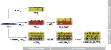
Figure 1. Schematic showing the synthesis procedures of all samples.
Download figure:
Standard image High-resolution imageThe first series of flat layers served as references to the host-guest electrodes and allowed analyzing performance-enhancing factors on simple model systems. This series comprised three samples, including a compact WO3 and a mesoporous Fe2O3:Sn layer coated onto FTO as well as a dual absorber photoelectrode prepared by depositing a WO3 overlayer onto a Fe2O3:Sn film. These samples are labeled 'WO3', 'Fe2O3' and 'Fe2O3/WO3', respectively. The second series demonstrated the performance-enhancing benefits of the host-guest architecture. A macroporous WO3 scaffold was infiltrated by Fe2O3:Sn and coated with an additional WO3 overlayer. In the remainder of the text, these samples are labeled 'mWO3', 'mWO3/Fe2O3', and 'mWO3/Fe2O3/WO3', respectively. It should be noted that WO3 is known to potentially fulfill several functions. At wavelengths below the optical absorption limit, WO3 acts as a photoabsorber. Due to its favorable band alignment, it can also act as a majority charge carrier collector of electrons generated in Fe2O3 [9]. Finally, WO3 can act as a surface treatment to Fe2O3 photoanodes, suppressing electron–hole recombination on the surface [5]. The samples in this study were prepared so that all three possible performance-enhancing effects could be studied systematically.
XRD patterns confirmed the successful synthesis of phase-pure Fe2O3:Sn in the hematite structure and of monoclinic WO3 (figure SI 1) (stacks.iop.org/MRX/4/016409/mmedia) [38, 39]. Other phases or reaction products could not be detected by XRD, SEM or TEM. In accordance with previous work by Dunn et al, cross-sectional analysis of mesoporous Fe2O3 layers showed ~50 nm thick mesoporous films composed of individual nanoparticles with an average size of ~40 nm × 80 nm (figures 2(b) and (c)) [28]. WO3, in contrast, forms ~100 nm thick, cracked layers composed of large, compact platelets between a few hundred nanometers and a few micrometers in size (figure SI 2). The Fe2O3/WO3 dual absorber retains these morphologies, with WO3 both infiltrating the Fe2O3 layer, with an accumulation at the FTO, and forming a ~50 nm thick layer on top (figures 2(a), (c) and (d)). By forming a compact top layer, WO3 decreases the exposed Fe2O3 surface area.
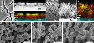
Figure 2. Morphological characterization. (a) Top-view SEM image of the Fe2O3/WO3 thin films. Fe2O3 is visible through cracks in the WO3 layer. ADF-STEM images and EDX maps of Fe2O3/WO3 are shown in (b) and (c). (d) Cross-section SEM image of mWO3/Fe2O3/WO3. ADF-STEM images and EDX maps of mWO3/Fe2O3/WO3 are shown in (e) and (f). Compared to the pure WO3 scaffold shown in (g), deposited Fe2O3 nanoparticles are clearly seen in (h). In (i) a SEM image of mWO3/Fe2O3/WO3 is shown. By depositing a WO3 overlayer, the whole structure is coated.
Download figure:
Standard image High-resolution imageIn contrast, the macroporous samples have an open, porous morphology (figure 2(d)). The macroporous WO3 scaffold forms a ~2.5 µm thick layer with ~150 nm wide pores (figure 2(g)). Even though the scaffold is distorted compared to a perfect inverse opal structure, it is continuous and reaches the back contact. This should be beneficial for charge transport. Hematite nanoparticles fully infiltrate the scaffold and are homogenously distributed throughout the whole film (figures 2(e) and (f)). An additional thin layer of Fe2O3 nanoparticles forms on the FTO substrate (figure 2(f)). In contrast to the flat layers, a WO3 overlayer fully infiltrates the scaffold and thinly coats WO3 scaffold and Fe2O3 nanoparticles alike without top layer formation (figure 2(i)).
The crystal structures of the materials were investigated by TEM. Monocrystallinity of hematite nanoparticles prepared by this synthesis procedure has previously been shown by Dunn et al [28]. Both the WO3 scaffold and the WO3 overlayer are highly crystalline, with mWO3 having domains of several hundred nanometers in size (figures 3(a) and (b)). In both Fe2O3/WO3 and mWO3/Fe2O3, an abrupt interface between Fe2O3 and WO3 without specific orientation relationships or amorphous phases was found (figure 3(c)).

Figure 3. HRTEM images of (a) the WO3 overlayer in Fe2O3/WO3 and (b) the WO3 scaffold. (c) Interface between Fe2O3 and WO3.
Download figure:
Standard image High-resolution imageLight absorption of all samples was assessed with UV–Vis measurements (figure 4). Like the photoelectrochemical measurements, they were done under substrate illumination.

Figure 4. UV–Vis, transmittance and reflectance spectra of mesoporous ((a)–(c)) and macroporous ((d)–(f)) samples.
Download figure:
Standard image High-resolution imageAs expected from the band gap, bare WO3 only absorbs light up to a wavelength of ~425 nm. In comparison, Fe2O3 absorbs light up to a wavelength of ~560 nm, consistent with a band gap of 2.2 eV, and thereby a much larger percentage of the solar spectrum. Of the flat layers, Fe2O3 absorbs more light than WO3 throughout the whole spectral range. In both flat and macroporous samples, more light is absorbed upon deposition of a mesoporous Fe2O3:Sn layer or a WO3 overlayer. Notable is the strong scattering contribution of both compact and macroporous WO3, which is reduced for all dual absorbers (figures 4(c) and (f)). As the UV–Vis spectra were acquired under substrate illumination, light must be backscattered by WO3 and absorbed by the Fe2O3 layer. WO3 acting as a reflective layer in the visible range (figures 4(c) and (f)) significantly increases the absorbance (figure 4(b) and (e)). Unfortunately, this increase in absorbance is not expected to contribute to the photocurrent, as it is above the absorption cut-off of both Fe2O3 and WO3. However, future studies, in which an additional photoabsorber is introduced, might benefit from this increase in scattering.
All samples were photoelectrochemically characterized by CV measurements under AM 1.5 illumination and by IPCE measurements (figure 5). Among the flat layers, Fe2O3 has a higher current density than WO3 (0.01 mA cm−2 at 1.23 V versus RHE compared to 0.08 mA cm−2 at 1.23 V versus RHE), which can be explained by increased light harvesting in the visible region. In accordance with the drop in light absorbance seen in the UV–Vis spectra, the IPCE spectrum of bare WO3 drops to 0% at ~425 nm, whereas the IPCE spectrum of Fe2O3 drops to 0% at a much longer wavelength of ~560 nm. Depositing a WO3 layer onto Fe2O3, thus creating a dual absorber, increases the current density threefold compared to Fe2O3 and 17-fold compared to WO3, with currents of 0.23 mA cm−2 at 1.23 V versus RHE and a maximum IPCE of up to 13% at 340 nm. This dual absorber not only outperforms the single components, but also the sum of current densities obtained from the individual absorber layers, suggesting that the increased performance cannot be explained solely by increased light absorption. Another important feature of the dual absorber photoanodes is a cathodic shift of the onset potential by nearly 200 mV. Such a shift is usually attributed to the reduction of loss pathways due to either charge transfer catalysis or suppression of surface recombination [40–42].

Figure 5. CV and IPCE measurements of flat ((a) and (b)) and macroporous layers ((c) and (d)) measured under AM 1.5 illumination. As the dark currents of all samples overlapped, only one measurement is shown.
Download figure:
Standard image High-resolution imageThe macroporous films show trends similar to the flat layer model systems (figure 5). The performance of the macroporous WO3 scaffolds (0.13 mA cm−2 at 1.23 V versus RHE) is strongly increased compared to WO3 flat layers. As shown by UV/Vis measurements, the deposition of Fe2O3 leads to increased light absorption in the visible range and a shift of the IPCE curve, increasing the current density up to 0.24 mA cm−2 at 1.23 V versus RHE. A substantial performance increase to 0.7 mA cm−2 at 1.23 V versus RHE with a maximum IPCE of 17% at 350 nm is achieved by depositing an additional WO3 layer. As for Fe2O3/WO3, CV measurements of mWO3/Fe2O3/WO3 show a steep current onset at 0.8 V versus RHE. mWO3/Fe2O3, which is also composed of both materials, does not show such a steep onset. The strong performance increases compared to flat layers could be explained by the increase in porosity and therefore surface area, or by the WO3 scaffold acting as a current collector as described in the literature [9, 29]. Of note is the strong performance rise when applying WO3 as a surface layer compared to having it as a scaffold. Interface-related effects such as suppressed recombination due to the WO3 surface layer could therefore play a major role. Another possible explanation is the role of WO3 as a scattering layer, which would increase the light harvesting efficiency of Fe2O3.
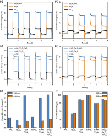
The photocurrents discussed so far were measured under AM 1.5 illumination. However, given the band structures of Fe2O3 and WO3 and based on our UV/Vis measurements, different processes are expected to take place under illumination with UV and with visible light (figure SI 3) [17]. Under UV illumination, electrons generated in Fe2O3 can be injected into WO3 and holes generated in WO3 can be injected into Fe2O3 (figure 6(a)), with the WO3 scaffold expected to reduce recombination by efficient charge transport to the FTO substrate. Light of a longer wavelength, however, only generates electron–hole pairs in Fe2O3, of which the electrons can, according to the band diagram, be injected into WO3 (figure SI 3). To gain further insight into the behavior of the dual absorber system, photocurrent transients were measured under chopped illumination with UV (365 nm) and blue (455 nm) light. Due to increased light absorption by both Fe2O3 and WO3 in the UV region, steady-state photocurrents acquired under UV illumination are consistently higher than those measured with blue light (figure 6(b)). WO3 is a highly efficient photocatalyst, leading to higher photocurrents than Fe2O3 under UV illumination [15]. Blue light, however, is not absorbed by WO3 (figure 4) and Fe2O3 reaches higher photocurrents.
Figure 6. Photocurrent transients of flat layers under (a) UV (365 nm) and (b) blue (455 nm) illumination at an applied potential of 1.23 V versus RHE. Photocurrent transients of the macroporous layers under 365 nm and 455 nm illumination are shown in (c) and (d), respectively. (e) Steady-state photocurrent densities under illumination with 365 nm and 455 nm light at a potential of 1.23 V versus RHE. (f) Transfer efficiencies under illumination with 365 nm and 455 nm light extracted from photocurrent transients measured at 1.23 V ca. RHE.
Download figure:
Standard image High-resolution image
Photocurrent transients reflect all processes influencing charge transfer and transport in the electrode (figure 6) [28, 43]. Upon illumination, movement of photo-generated holes to the surface leads to a charging or displacement current. If holes accumulate, either due to slow surface kinetics or due to slow electron transport to the back contact, they recombine with electrons, and the initial photocurrent decays to a lower steady-state photocurrent. For Fe2O3, this leads to a characteristic 'spike and overshoot' photocurrent, whereas fast surface kinetics and good electron conductivity of pure WO3 lead to a rectangular transient form suggestive of complete charge carrier extraction [43]. By depositing Fe2O3 onto a WO3 scaffold, the difference between initial and steady-state photocurrent decreases compared to Fe2O3 and deposition of an additional WO3 layer brings the shape of the photocurrent transient even closer to a rectangle. As expected from the fast surface kinetics and good charge transport properties the material is known for, both WO3 and mWO3 have transfer efficiencies of 100% [15]. In comparison and in accordance with previous work by Dunn et al, Sn-doped Fe2O3 has a transfer efficiency of 41% [28]. The transfer efficiency can be improved to 75% by depositing the Sn-doped Fe2O3 layer onto a WO3 scaffold. In line with discussion in the literature, the WO3 scaffold could act as a charge collector and thereby increase the electron diffusion length [9, 29]. In comparison, surface treatment by the deposition of an additional WO3 layer has a greater effect on the transfer efficiency than the introduction of a WO3 scaffold and increases the transfer efficiency to 85 and 88% for flat Fe2O3/WO3 and macroporous mWO3/Fe2O3/WO3, respectively. The improved performance might stem from an enhanced rate of Faradaic reactions on the interface due to the surface treatment with WO3. For both illumination wavelengths, photocurrent densities reached by the dual absorbers, regardless of whether WO3 was applied as a surface layer or as a scaffold, are very similar. This is in contrast to measurements under the full AM 1.5 solar spectrum, where a much larger difference in photocurrent densities was observed for the different architectures. This can presumably be explained by a complex interplay of several factors, such as faster surface kinetics, improved current collection and enhanced light absorption, in which WO3 beneficially influences Fe2O3.
4. Conclusions
To systematically analyze the effects of WO3 on Fe2O3 for photoelectrochemical water splitting, dual absorbers were prepared with WO3 as a scaffold and/or as a surface layer. Both approaches significantly increased the performance, validating both the host-guest and the surface layer approach. By combining them, current densities of 0.7 mA cm−2 at 1.23 V versus RHE under AM 1.5 illumination with an IPCE of 17% at 350 nm were reached. The performance increase was investigated by CV, IPCE, photocurrent transient and UV–Vis measurements and we could identify several beneficial effects responsible for improved charge carrier generation and transport. WO3 strongly reflects visible light which in the dual absorbers is then absorbed by Fe2O3, resulting in increased light harvesting and thus higher photocurrents. Compared to Fe2O3, a cathodic shift of the onset potential from 1.0 to 0.8 V and an increase in transfer efficiencies, reaching up to 88%, were measured. We conclude that the investigated device architecture is a promising approach for the design of Fe2O3/WO3 dual absorber photoanodes by combining different beneficial effects of different materials to produce substantially improved devices.
Acknowledgments
The work was supported by the German Research Foundation (DFG) via the priority program SPP 1613, the Nanosystems Initiative Munich (NIM) and LMUexcellent, the Bavarian research network 'Solar Technologies Go Hybrid', and the Center for Nanoscience (CeNS). We thank the students Zachary Edelen and Marina Polo Collado for participating in the research. Steffen Schmidt and Halina Dunn are gratefully acknowledged for insightful discussions.