
Abstract
Heterostructures (HSs) based on two-dimensional transition metal dichalcogenides (TMDCs) are highly intriguing materials because of the layers' pronounced excitonic properties and their nontrivial contributions to the HS. These HSs exhibit unique properties that are not observed in either of the constituent components in isolation. Interlayer excitons (IEs), which are electron–hole pairs separated across the HSs, play a central role in determining these HS properties and are of interest both fundamentally and for device applications. In recent years, a major focus has been on understanding and designing HSs composed of two or more TMDC materials. Less attention has been paid to HSs composed of one TMDC layer and a layer of perovskite material. A central challenge in the understanding of HS properties is that basic measurements such as optical spectroscopic analysis can be misinterpreted due to the complexity of the charge transfer dynamics. Addressing these aspects, this review presents an overview of the most common and insightful optical spectroscopic techniques used to study TMDC/TMDC and TMDC/halide perovskite HSs. Emphasis is placed on the interpretation of these measurements in terms of charge transfer and the formation of IEs. Recent advances have started to uncover highly interesting phenomena, and with improved understanding these HSs offer great potential for device applications such as photodetectors and miniaturized optics.
Export citation and abstract BibTeX RIS

Original content from this work may be used under the terms of the Creative Commons Attribution 4.0 license. Any further distribution of this work must maintain attribution to the author(s) and the title of the work, journal citation and DOI.
1. Introduction
Two-dimensional (2D) semiconductors and their heterostructures (HSs) are rapidly growing fields of broad interest due to their interesting exciton physics and promising future device applications [1, 2]. These layered materials are strongly bound within the atomic layers, but more weakly bound by Van der Waals forces between layers. In recent years it has become clear that monolayers of transition metal dichalcogenides (TMDCs) exhibit interesting physics due to the combined effects of confinement and reduction of dielectric screening. The latter results in strongly bound excitons, with binding energies of around 500 meV in the monolayer materials [3–5], causing the excitons to be observable at room temperature. The TMDC monolayers typically have optical bandgaps between 1 eV and 3 eV—spanning the near-infrared and visible ranges of the electromagnetic spectrum [3]. However, control over excitons is difficult due to their charge neutrality. Therefore, various ways of influencing and enhancing excitonic behaviour are currently under investigation. Among these, HSs, formed by stacking different monolayer TMDCs, attracted much interest due to their great potential. Various material combinations allow for more control over the charge carriers in these HSs, while still leveraging the interesting exciton properties of these materials. These properties mean that 2D TMDCs and their HSs have potential applications in high-performance photodetectors and as components of solar cells [6–12].
Interlayer excitons (IEs) are excitons whose charges are spatially separated across the stacked layers of the HS; their observation has garnered justifiable interest within the community [13–16]. Despite their importance for understanding the charge carrier and decay dynamics, interpretation of their experimental signatures remains challenging due to the already rich variety of other excitonic states in these HSs.
In this review, we present a summary of the most common optical spectroscopic tools applied to identify the presence of excitons and their nature in TMDC HSs. These techniques include steady-state photoluminescence (PL) spectroscopy, time-resolved PL (TRPL) spectroscopy, and ultrafast transient absorption (TA) spectroscopy. These key experimental methods, supplemented with additional measurements such as absorption and reflection spectroscopy, Raman spectroscopy, transmission electron microscopy (TEM) and electrical assessment methods, also discussed, can provide important insights into the charge carrier and exciton states and their dynamics within the HS. The synthesis methods of TMDCs and their HSs are a vast topic on their own, for which we refer readers to existing reviews [17–25].
We consider two types of HSs, those composed of purely TMDC layers (TMDC/TMDC) and those with one TMDC monolayer and a layer of semiconducting perovskite materials (TMDC/PMs). We review the experimental insights into the energy- and charge-transfer processes that can occur in TMDC/TMDC and TMDC/PM HSs and how these processes result in the formation of IEs. Because of their complexity and the diverse possibilities of interpretation, several complementary techniques are needed to conclude on the processes at play. Next to true TMDC/TMDC HSs, we also include the investigation of Janus monolayers, for which the chalcogenide layers above and below the metal plane are composed of different chalcogen atoms, and discuss the interpretation of their experimental features.
For the most trustworthy interpretation of the data, it is imperative to consider the different charge carrier recombination pathways that may occur in TMDC HSs and how these can affect the optical properties of the materials. These pathways can arise due to defects, vacancies and grain boundaries within the material, leading to non-radiative recombination. Identifying and differentiating how these pathways might interact, or be confused with charge- and energy-transfer processes is an important issue that is discussed in the final section of this work. Understanding these alternative mechanisms is crucial for an accurate interpretation of the spectroscopic results. The review is structured as follows: starting with a general introduction to the physics of semiconducting TMDCs in section 2, we provide a brief overview of the HS properties and experimental signatures of excitons in TMDC/TMDC HSs in section 3. We then discuss the recent work in mixed TMDC/PM HSs in section 4, before discussing alternative processes in section 5.
2. TMDC monolayers
TMDCs—with chemical formula MX2, where M is a transition metal and X is a chalcogen atom—can vary from insulators to conductors, depending on their elemental composition and phase. Bulk TMDCs were studied and extensively described decades ago, most notably by Wilson and Yoffe [26], but only came back into focus in 2010 through the seminal work by Mak et al [27], after Novoselov et al showed it is possible to cleave graphite, and other layered crystals, down to the monolayer with a micromechanical cleavage method [28]. There are several reviews on TMDC monolayers and their HSs, so only a brief classification is given here. For further background, the reader is referred to these earlier reviews [16, 17, 28–30]. The most common configurations for the semiconducting TMDCs are the trigonal prismatic (2H) and the octahedral (1T) phases. These phases differ by the stacking order of the chalcogen on the transition metal atom, as shown in figure 1(a). The 2H phase is stacked in an X–M–X sequence, where the chalcogen atoms are positioned along the same vertical coordinate across different X layers [31], while the 1T phase is stacked in X–M–X' sequence, with the two chalcogen layers displaced from each other.
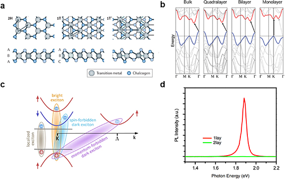
Figure 1. (a) Schematic of a monolayer TMDC with trigonal prismatic,  (left), distorted octahedral,
  (centre) and dimerized
  ' (right) phases. Reproduced from [31], with permission from Springer Nature. (b) Representation of the electronic bandstructure changes in MoS2 upon a change in thickness. Reprinted with permission from [44]. Copyright (2010) American Chemical Society. (c) Various possible transitions in TMDCs, showing both optically allowed, and optically forbidden transitions. Reproduced from [16]. CC BY 4.0. (d) Room-temperature photoluminescence spectra of mono- and bi-layer MoS2, showing the drastic changes induced by layer thickness. Images were adapted from [16, 31, 44] and [27] for (a) to (d), respectively. Reprinted with permission from [27], Copyright (2010) by the American Physical Society.
Download figure:
Standard image High-resolution image2.1. Electronic bandstructure
While graphene and the prototypical monolayer TMDCs such as MoS2 and WSe2 have a similar honeycomb crystal structure, their optoelectronic properties are vastly different [17]. These properties are determined by the specifics of their electronic bandstructures, which differs significantly between graphene and the TMDCs. The difference roots in two fundamental properties: (i) The heavier transition metals in TMDCs induce strong spin–orbit coupling (SOC), and (ii) the specific two-atom system in the MX2 (M: Mo, W, X: S, Se) structure breaks inversion symmetry. These fundamental properties of TMDCs result in the opening of a bandgap and the splitting of the K and K' valleys in the electronic bandstructure. Furthermore, a direct-to-indirect bandgap transition results upon stacking several TMDC layers due to specific orbital contributions of the metal and chalcogen atoms, see figure 1(b). Specifically, there are three valleys of interest in the electronic bandstructure of TMDCs: at the Γ, the K and the K' point in the Brillouin zone. A major distinction between the Γ and the K-valleys is in the aforementioned relative contributions of the metal and chalcogen orbitals, which cause the direct-to-indirect bandgap crossover due to the more out-of-plane p-orbital character of the bands at the Γ and Λ points [32–34]. With increasing number of layers, the states at the Γ point are strongly affected, as shown in figure 1(b). As a result, the prototypical MoS2, MoSe2, WS2 and WSe2 have room-temperature bulk electronic bandgaps of 1.2, 1.1, 1.4 and 1.2 eV, respectively, while their respective monolayers have 2.5, 2.3, 2.6 and 2.2 eV [29, 35]. However, the monolayer values are very sensitive to the measurement geometry and generally, it is more difficult to extract electronic band energies rather than optical bandgap energies, which are related to the excitonic states in these materials.
The distinction between K and K' valleys is due to the combined effect of SOC and broken inversion symmetry, causing opposite spins of states in these two valleys [33, 36]. Furthermore, the SOC causes splitting of valence and conduction bands in predominantly these K and K' valleys, as shown in figure 1(c) [31]. It was expected that these effects cause perfect spin-valley polarization protected by the above symmetry considerations [37]. However, in practice, the electron–hole exchange interaction causes rapid valley depolarization, even at cryogenic temperatures and in high-quality samples [38, 39]. This suggests that the realization of the often-discussed spin-valleytronics, which aims to use the spin- and valley-degrees of freedom next to the electric charge for solid-state applications, is not very practical in TMDC monolayers. Quantitatively, the energy offsets due to splittings of the valence bands at the K points are predicted to be 148, 183, 426 and 456 meV, respectively, for MoS2, MoSe2, WS2 and WSe2 monolayers, while those for the conduction bands are, respectively, 16, 35, 3 and 3 meV [32, 40]. This spin-splitting can render the lowest energetic transition between the valence and conduction band at the K-points spin-forbidden, leading to dark states [40]. The existence of these dark states has been shown [41], and it turns out that molybdenum-based dichalcogenides have a spin-allowed lowest transition. In contrast, the lowest transition for tungsten-dichalcogenides is spin-forbidden. This affects the optical properties to a great degree [42, 43].
2.2. Excitons
Another important aspect of the transition from bulk to monolayer is the dielectric screening of electric charges by the material. This screening is drastically reduced from bulk to monolayer, resulting in more strongly bound states of electrons and holes, called excitons [45, 46]. While these bound states also exist in the bulk, their binding energy is enhanced in monolayers, where it can significantly affect the energetics of the electronic bandstructure. In this case, a simple band model of free carriers is not applicable any more, and ultimately, many of the optoelectronic properties of TMDCs become dominated by the properties of excitons [27]. Experimentally, this manifests as sharp resonances in the optical spectra. At the same time, the symmetry considerations causing the spin-split states still apply. As a result, TMDCs display excitons at the valence and conduction band spin-split states, termed A and B excitons, respectively, for the lower and higher energy states of the direct ( ) bandgap transition [26]. These A and B excitons represent the bright states. Besides these bright states, there might be spin-dark exciton states with energies above or below the bright states, depending on the exchange- and spin–orbit interactions [40]. Moreover, momentum-indirect transitions (
 ,
,  ) in the bandstructure contribute additional bound states, but optical transitions to these states have much lower oscillator strengths due to the momentum mismatch [16], so they are much less frequently observed. An overview of the possible transitions is given in figure 1(c).
Because of the high exciton binding energies, excited states of the excitons can be experimentally observed. As the excitons are composed of a positively-charged hole and a negatively-charged electron similar to a hydrogen-like atom, their excited states are commonly modelled by a simple Rydberg-like formula. The excited exciton states are then labelled 1s, 2s, 2p, etcetera, following hydrogenic atoms, and they can contribute to the optical spectra. These states lie between the 1s excitonic ground state and the continuum band, where the energy difference between these two extremes is called the exciton binding energy. Due to selection rules, however, only the s states can be optically excited or probed in the absence of any external fields [47, 48]. Excitingly, recent work suggests that TMDC monolayers show signs of band topology, which would alter the optical selection rules [49]. Mapping out the excited-state energies is one of the common ways of deducing exciton binding energies, as these energies asymptotically approach the continuum band [50].
Finally, in the presence of extra free charges or other excitons, exciton complexes such as trions or bi-excitons can form resulting in extra observable states. These extra free charges can occur due to defects, doping or high excitation fluences [51–54], resulting in binding energies in these complexes on the order of 10s of meV, much lower than those of the excitons, yet in some cases high enough to be observed at room temperature. Besides these common excitonic states, many more states can show up in the optical spectra, such as bulk-specific excitons [55], phonon replicas [56, 57], polaritons [58], and defect emission [59], among others. Many of the mentioned phenomena have by now been established in the prototypical Mo- and W-based TMDCs; yet, even in these materials, the richness of the excitonic states makes it difficult to uniquely assign them to spectroscopic features. For the less established TMDCs, compositional changes, such as in the group IV TMDCs (M: Hf, Zr; X: S, Se), alter the bandstructure [60]. Furthermore, reduced crystal symmetries might cause additional degrees of freedom to appear, such as horizontal linear optical polarization in the case of group VII ReX2 (X: S, Se) compounds [61]. Especially in these less-studied materials, there is still much to discover regarding the nature of their excitonic properties.
2.3. Recombination processes
While there are many excitonic states present, typically only one of them, the lowest allowed transition, is observed in PL spectra at room temperature, see for example figure 1(d). Nevertheless, there are numerous radiative and non-radiative recombination pathways in TMDC monolayers that can affect the average decay rate (figure 2). The dominant pathways can vary depending on the temperature, density and type of defect states present, as well as the applied power density [62]. Under low excitation intensities, exciton–phonon scattering and radiative coupling are the dominant recombination processes. Under higher excitation intensity, exciton–exciton scattering also becomes prominent. One common way of characterising material quality is through PL quantum yield (PLQY) measurements, where low PLQY values indicate that non-radiative dominate over radiative decay channels. Attaining high PLQY in these materials remains a challenge, as a significant fraction of excitons typically recombines non-radiatively via intrinsic trap states, mostly due to chalcogen vacancies [63–66]. This limits the PLQY to an order of 1% (0.1% in MoS2, 6% in WS2) and radically minimises the feasible optoelectronic applications of TMDC monolayers [67]. On the other hand, the combined effects of confinement and reduced screening tend to increase light absorption at the exciton lines and enhance the PLQY in monolayers compared to the bulk [16, 27, 44, 68]. Consequently, these 2D materials are strong candidates for applications in next-generation optoelectronic devices [69–72].
Figure 2. Radiative and non-radiative recombination pathways in monolayer TMDCs. Here, exciton, trion and biexciton decays can all be radiative and are associated with their own spectral characteristics. The other processes are scattering processes that change occupations of excitonic states, which might be monitored under the right experimental conditions with transient absorption spectroscopy, for example. Reproduced with permission from [62].
Download figure:
Standard image High-resolution imageDepending on the application in mind, quantum-yield limitations might be overcome by stacking a TMDC monolayer with a material with high quantum efficiency—for example, a perovskite semiconductor. TMDC monolayers can also be stacked with other TMDC monolayers, which can alter the overall excitonic properties of the materials. Naturally, the abundance of phenomena already present in monolayers provides a very versatile platform for material tunability once these monolayers are combined into HSs. For example, the valley polarization, which is lifted in monolayers due to the electron–hole exchange interaction, can be more protected in HSs due to small wavefunction overlap for the IE [73–75]. Before using these sophisticated effects in applications, however, much work remains to be done to elucidate the structure–property relations of HSs. In the following sections, we briefly touch on the very rich field of TMDC–TMDC HSs before going more deeply into recent results of mixed HSs.
3. Heterostructures
2D TMDC monolayers can be stacked on top of each other, bound by Van der Waals interactions to form either homostructures—where the layers are composed of the same material, or HSs—where the TMDC monolayers are made up of different materials [76, 77]. The HSs can be fabricated using a variety of techniques, the most common of which include mechanical exfoliation by either a wet or dry transfer process, followed by contact transfer and chemical vapour deposition (CVD). Microscope images of HSs fabricated by mechanical exfoliation are shown in figure 3 [28, 78]. As the HSs are bound by Van der Waals forces and do not involve atom-specific bonding, there is a myriad of possible combinations of Van der Waals HSs. For this reason, interest in HSs has been continuously rising over the past years. Between 2012 and 2022, for example, there have been on average 860 additional works published compared to the previous year [79]. These works include the fabrication of 2D TMDC/TMDC HSs, along with 2D TMDCs that are stacked with entirely different materials into HSs, such as 2D perovskite microplates and 0D perovskite quantum dots (QDs), as we will discuss later.

Figure 3. Optical microscope images of two heterostructures. Both heterostructures were fabricated using mechanical exfoliation of the individual materials and subsequent stamping. (a) A heterostructure of the two semiconductors MoSe2 and WSe2. Reproduced from [14], with permission from Springer Nature. (b) A heterostructure of MoS2 and the insulator hBN, [80] John Wiley & Sons. © 2019 WILEY-VCH Verlag GmbH & Co. KGaA, Weinheim.
Download figure:
Standard image High-resolution imageThe potential for stacking different materials, without a strong necessity of lattice matching, promises highly tunable HSs with properties that can be vastly different from any of the constituents. An important ingredient in understanding HSs is their band alignment, which results from the respective energies of the electronic bands of the two materials, and determines whether charge or energy transfer occurs between them, as discussed below. Furthermore, some HS properties result from the formation of defect states, which can lead to substrate effects on interlayer interactions, for example [81–83]. Finally, an intriguing aspect of HSs is the formation of IEs, formed as a result of charge transfer across the two materials. These IEs differ significantly from excitons in single monolayers, as the constituent charges of IEs are separated, located in the opposing layers. Furthermore, besides having the freedom of stacking different compounds, it turns out that the angle under which the two, or more, layers are stacked affects the optoelectronic properties of the HSs to a great degree. These stacking-angle dependent systems are called Moiré HSs, and they will be discussed in more detail below. In any case, due to the specific band alignments, the stacked HS can be thought of as an entirely new material compared to the individual constituents and hence opens an entirely new field in optoelectronics.
3.1. Band alignments
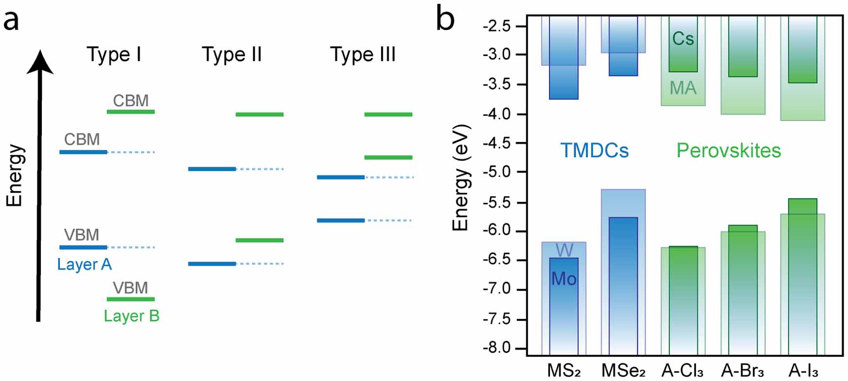
The relative energy levels of the electronic bands of the stacked materials give rise to characteristic band alignment, which determines much of the properties of the HS. One can distinguish three types of alignments, as summarised in figure 4(a): in a type I alignment, the valence band maximum (VBM) and conduction band minimum (CBM) of material A are sandwiched by the valence and conduction band extrema of material B. In this case, both electrons and holes tend to diffuse into the material with the smaller bandgap, and thus energy transfer can occur from material B to A. In a type II alignment, the bands are staggered, meaning that both the VBM and the CBM of one material lie above those of the other material. This favours charge separation at the interface of the two materials, where electrons and holes experience opposite driving forces, and thus get transferred into opposite layers. This alignment is the one required for photodiodes or solar cells to separate photo-generated charges. A rare case is the type III HS where the energies of both valence and conduction band extrema of one material lie above the CBM of the other, creating a so-called broken gap. Because electrons and holes now experience a large potential barrier at the interface, charge transport is essentially only possible due to tunnelling, and thus this type of band alignment can be used to create tunnelling junctions [84–86].

Figure 4. (a) The three types of heterostructures. Solid lines indicate the energies of bands for material A (blue) and material B (green), with dashed lines added merely as a guide to the eye. Depending on the relative energies of the bands, type I, II and III can be distinguished. (b) Band energies of common TMDCs (blue) and lead-based perovskite materials (green). The band energies of the TMDCs are calculated using the  method [87], with solid boxes indicating molybdenum compounds and transparent boxes indicating tungsten compounds. The perovskite materials have the chemical formula APbX3, where solid boxes show perovskites with the A = Cs cation [88], and transparent boxes show band energies with A = methyl ammonium (MA) compound [89], and X is a halide (Cl, Br, I) as indicated.
Download figure:
Standard image High-resolution imageThe band alignment is generally calculated by density functional theory (DFT) or by the single-shot perturbative G0W0 approximation to determine the work functions [87]. The G0W0 is also referred to as the dynamically screened interaction; in this approximation, the multi-body electron–electron interactions are captured in a quantity called the electron self-energy and are calculated as a product of Green's function (G) with the screened interaction (W) [90–92].
Experimental methods such as microbeam scanning tunnelling microscopy (STM), high-resolution x-ray photoelectron spectroscopy (XPS), ultraviolet-visible (UV–VIS) spectroscopy and angle-resolved photoemission spectroscopy can then be used to extract the valence band and conduction band offsets and the electronic band gap of the material [93–95].
From the obtained energy values, the band alignment of the HS can be determined [96, 97]. Figure 4(b) shows an overview of band energies for the most common TMDCs, calculated using the  method [87], and PMs, obtained through experimental [88], and DFT techniques [89].
3.2. Interlayer excitons in TMDC/TMDC heterostructures
TMDC HSs were first reported by Fang and co-workers in 2014, who fabricated a WSe2/MoS2 structure [13] by mechanical exfoliation and subsequent stacking of the exfoliated monolayers on top of each other. This technique is now common throughout the literature and allows for convenient identification of the separate monolayers, and the HS region where they overlap, using techniques like room-temperature optical microscopy, Raman spectroscopy, TEM and photoemission electron microscopy. With absorption measurements, the authors showed that the HS region exhibited an absorption profile that is roughly a linear combination of the individual monolayers. Contrastingly, the PL measurements showed quenching of the main exciton peaks of both materials and an additional lower-energy peak. These results suggested that the extra PL peak is not due to a shift of the main exciton lines, but rather due to the HS. The authors attributed this peak to the relaxation of electron–hole pairs bound across the interface; they showed that the PL signal of this feature decreases as hexagonal boron nitride (hBN) layers are introduced between the WSe2 and MoS2 layers, supporting the idea that this PL feature originates from interface-separated bound charges. The interfacial electron–hole pairs from this interpretation came to be called IEs and result from HSs of a type II alignment. Subsequent work on a MoSe2/WSe2 HS similarly identified a lower-lying PL peak, see figure 5, and found that this state is long-lived, with a lifetime of 1.8 ns [14], much longer than the typical PL lifetimes of excitons and trions, which are on the order of 10 ps for TMDC monolayers [98]. Such slow radiative recombination has also been observed in MoS2/MoSe2 HSs [99], indicating that the increased average lifetime measured for TMDC/TMDC HSs is a general property of IEs in group-VI TMDCs. Since then, similar PL signatures have been observed in several other works [100–103], and the measurements were expanded to temperature-dependent PL [102]. In addition, electrostatic gating was introduced to tune the energy of the IE, as shown in figure 6. The vertically separated charges across the stacked layers are associated with an electric dipole moment along the out-of-plane direction, which can be modulated by an electric field induced by an electrostatic gate. Such a static dipole moment is not expected from defect states, thus the observation of electrical modulation of the PL feature provides important support to the existence of IEs [102].

Figure 5. (a) Band alignment and formation of an interlayer exciton in a MoSe2/WSe2 heterostructure. (b) Photoluminescence spectra , taken at 20 K, of the WSe2 and MoSe2 monolayers and their heterobilayer. The peak at 1.35 eV was attributed to the interlayer exciton emission. Reproduced from [14], with permission from Springer Nature.
Download figure:
Standard image High-resolution image
Figure 6. (a) PL spectra indicating the formation of interlayer exciton in a MoS2/WSe2 based on the quenching of the intralayer exciton emission. (b) Variation in the PL emission band of the interlayer exciton in the same HS as a function of temperature. (c) A gated device was fabricated in order to apply an out-of-plane electric field to the HS. (d) PL spectra of the interlayer exciton as a function of the applied voltage to the gated device. Reprinted with permission from [102], Copyright (2019) by the American Physical Society.
Download figure:
Standard image High-resolution imageCrucial theoretical insight came from studies on a MoS2/WSe2 HS, where PL spectroscopy was combined with DFT calculations to show that the lower-energy IE feature in the PL spectra could be explained by a  transition, showing that the exciton is not just characterized by a lower spatial overlap of the charges due to the layer separation, but its recombination also involves a momentum-indirect transition [104]. Similarly, another study attributed spectroscopic features of TMDC HSs to momentum-indirect transitions [105], although a MoSe2/WSe2 HS was suggested to have interlayer features comprised of both direct and indirect transitions [106]. Such momentum-indirect transitions are consistent with the direct-to-indirect transition in bilayer homostructures as the orbital character of TMDCs at the Γ and Λ points have significant out-of-plane character [32–34]. These points in the electronic bandstructures of the HSs are sensitive to both interlayer distance and interlayer stacking angles and can thus be altered by stacking. These features support the observations of predominantly momentum-indirect IEs and are consistent with their long PL lifetimes [74].
Detailed studies on the formation and decay kinetics of excitons in TMDC/TMDC HSs were first performed by Hong and co-workers [107]. They used pump-probe spectroscopy on the femtosecond time scale along with PL measurements to study the ultrafast dynamics of charge transfer across the interface, inspired by previous studies, which demonstrated ultra-fast charge transfer kinetics in organic heterostructures that were also bound together by Van der Waals forces [108, 109]. Hong's work focused on MoS2/WS2 layers that exhibit a type II band alignment. Low-temperature (77 K) and room-temperature PL measurements showed strong emission intensities in the separated monolayers, but PL quenching in the combined HS, indicating possible charge transfer. When resonantly pumping at the energy of the MoS2 A exciton and probing the absorption of the HS, the authors found a pump-induced decrease of absorption in both materials, even though the A and B exciton lines of WS2 had energies far above the pump energy. This pump-induced decrease of absorption is indicative of charge transfer since the generated charge carriers after transfer occupy states which reduce the absorption. Confirming that the TA signal resurges in isolated WS2 then consolidated the interpretation of charge transfer from MoS2 to WS2. Additionally, by varying the delay time of the probe, the authors determined that holes from the MoS2 layer had migrated into the WS2 layer within 50 fs after irradiation by the pump. These kinetics were observed both at 77 K and at room temperature. Other works, such as that of Ceballos and co-workers, yielded similar results for a MoS2/MoSe2 heterobilayer [110]. These examples indicate how optical methods can provide insight into charge transfer processes in the TMDC/TMDC heterobilayers [107, 110, 111].
IEs typically recombine at a much slower rate than intralayer excitons as a result of the reduction in the spatial overlap of their wavefunctions [112–114]. The average IE lifetime spans from the order of 50 ps to 1.5 ns, depending on the stacking nature of the layers and the nature of exciton recombination [115]. Hence, recombination lifetimes can be prolonged not only by varying the stacking order but also by measuring at lower temperatures, measuring with a different twist angle, increasing spatial separation of the monolayers and synthesising the HS with a different technique [116, 117]. Furthermore, differences in the photoluminescence spectra and kinetics between TMDC HSs and their monolayers can also be ascribed to surface defect states and other radiative trap states [63, 113, 118–120]. Therefore, single-experiment characterisation, using PL or TRPL alone, is generally insufficient to conclude on the formation of IEs. An additional powerful technique is cathodoluminescence (CL), in which electrons are used to locally excite charge carriers to obtain insight into their local radiative decays, achieving superior spatial resolution in photoemission mapping. While this technique has been applied to IEs to identify and isolate them from intralayer excitons [121, 122], comprehensive work including both steady-state and time-resolved CL is limited, but could provide further insights on the nature of IEs.
3.3. Moiré excitons
One of the critical tuning parameters in stacked TMDC HSs is the relative angle of orientation between two layers. This twisting angle plays a pivotal role in shaping the electronic properties of the resulting structure. For example, in bilayer graphene, the stacked material undergoes a transformative shift into a superconducting state at a highly specific twisting angle, commonly termed the 'magic angle' [123]. The intricate electronic effects induced by the twisting angle create a Moiré pattern—a superlattice formed by the periodic interference between the two layers. Under a specific stacking angle, this leads to the emergence of a flat electronic band, intensifying electron correlations and facilitating superconductivity in the specific case of bilayer graphene [124, 125]. In TMDC HSs, several works have explored the effects of variable stacking orientation and twisted layers. This exploration has revealed a new class of quasiparticles known as Moiré excitons [126–128]. The Moiré excitons can be interlayer or intralayer in nature. These twist-induced excitonic states exhibit enhanced binding energies and, provided that the Bohr radius of the Moiré exciton is smaller than the Moiré pattern itself, long-range spatial periodicity—properties which are distinct from excitons found in individual TMDC layers [129]. In addition to their formation, the precise behaviour of the Moiré excitons is significantly affected by the difference in the twist angle between the TMDC bilayers [130, 131]. For example, with an increasing twist, regions of constructive interference in the Moiré pattern become more localised, which in turn affects the spatial distribution of the excitons themselves. Furthermore, changes in the electronic band structure due to variations in the Moiré pattern will directly impact the absorption and emission characteristics of the Moiré excitons—an increase in twist angle will lead to shifts in the optical signatures associated with Moiré excitons [132, 133].
We note that PL and TRPL are not the only optical techniques applied to study the precise properties of IEs. Reflection spectroscopy has been used as an additional assessment tool to provide further insight into the excitonic nature. As an example, optical spectra, measured at 10 K, were employed to study the twist-angle dependent properties of the IE in the WSe2/WS2 TMDC HS under different angles of orientation, after the presence of an IE peak was established from PL [126]. The authors showed that a near-zero twist angle contributes to a much stronger enhancement of the interlayer excitonic peak than a larger angle. This is attributed to the Moiré pattern at the near-zero twist angle generating distinct Moiré exciton states, which are then visible in the reflectance spectra. Notably, the reflectance spectra were directly compared to the PL excitation (PLE) spectra, and found to yield the same excitonic features. With properties such as the ones discussed above, Moiré excitons in TMDC heterobilayers have expansive potential applications in the fields of 'twistronics' (utilising the twist-dependent electronic properties of the system), nano-photonics and quantum information [134, 135].
3.4. Janus layers
Over the past few years, alloying has emerged as a powerful technique to tune the structure and optoelectronic properties of TMDCs. In this fabrication technique, layers of  or
or  are synthesised by varying the composition (y) of the metal (
 ) or chalcogen (
 ) atoms [136–138]. By controlling the alloying composition in each individual layer, fundamental properties such as bandgap and effective mass can be effectively modified [136, 139, 140]. Both theoretical and experimental studies have shown composition-dependent bandgaps in the TMDC alloys and the obtained results have opened possibilities of bandgap engineering [136, 141–143]. Since the alloyed layers can be used for stacking, this further expands the space of HS possibilities for the TMDCs.
Interesting examples of alloyed layers are Janus monolayers, where the controlled mixing of chalcogen atoms leads to bottom and top chalcogen planes of different composition. This results in an out-of-plane dipole, as for the layered HSs [144]. However, due to the complete absence of any real stacking, there is no possibility of momentum mismatch, and the optical transitions tend to be at energies in between those of the pure compounds [145]. One study fabricated WSSe/MoSSe and WSe2/WSSe HSs by a combination of plasma-induced vacancy formation coupled with a CVD process [145]. The PL spectra of the HSs clearly showed that the HSs exhibit PL from both layers, yet no clear conclusions were drawn on charge transfer effects. Another study on stacking Janus monolayers investigated the effects of the built-in field from the different chalcogen planes on charge transfer rates in a WSSe/WS2 HS and found that the Janus-induced electric field can function as an additional potential barrier, prohibiting charge transfer, even when the type II band alignment suggests its possibility [146]. This makes the charge transfer rate directional and dependent on the stacking sequence. A further alloying possibility is the alloying of the metallic component, followed by HS formation, creating layers with different metallic constituents. This has been explored briefly in early work where HS alloys were directly grown by CVD [147]. While the HS composition was indeed verified through Raman and PL techniques, however, no clear analyses were performed on charge transfer, leaving it as an interesting future research direction. These examples show that, already within the TMDC family, there is a lot of design space for fabricating HSs with diverse functionality. This design space can be further expanded by stacking TMDC monolayers with completely different compounds. This direction will be discussed in the following section, focusing on TMDC/perovskite HSs.
4. TMDC-perovskite heterostructures
The performance of 2D TMDC/TMDC HSs in optoelectronic devices is limited by low light absorption, related to their single atomic layers, which is particularly undesirable for photovoltaic applications. One way to improve the overall absorbance is to replace one of the TMDC layers with a strongly absorbing material. This strategy has been demonstrated for organic materials, carbon nanotubes and QDs [148–152]. As the potential number of candidate materials for forming HSs with TMDCs is huge, in this review we focus specifically on HSs of TMDCs with halide PMs. Perovskites can effectively enhance absorbance, even though the absorption coefficient of a monolayer of a typical perovskite is roughly the same as that of a TMDC monolayer [153]: nevertheless, as their carrier transport is very efficient, thick perovskite layers can be used for the absorption, absorbing sufficient amount of light to create charge carriers, which can then migrate to the HS interface. In the following, we will first review the most basic properties of perovskite structures, before we go into more detail about perovskite/TMDC HSs.
4.1. Perovskite
We will primarily focus on HSs consisting of the conventional perovskite with the ABX3 crystal structure, wherein A corresponds to a small cation, such as Cs+ or methylammonium (MA+), B corresponds to a large cation, such as Pb2+ and Sn2+, and X is a halide anion or some mix of halide anions. Much has been written on the chemical and optoelectronic properties of these perovskites and we refer the reader to some in-depth reviews [154–158]. Briefly, semiconducting inorganic CsPbX3 materials, where X is a halide atom, have been known to crystallise in the perovskite structure since the 1950s, [159], and the prototypical organic–inorganic compound of methyl-ammonium lead halide (MAPbX3) was subsequently described in the 1970s [160]. Differences in A-site cations (MA versus Cs) not only result in structural differences and relative differences in stability (CsPbBr3, which is the more stable of the two, is typically found in the orthorhombic phase at room temperature, while MAPbBr3 is found in the cubic phase) but also results in optical and optoelectronic changes in the material—for example, the band gap of MAPbBr3 tends to be lower than CsPbBr3 [161, 162]. Going from bulk to confined systems, the 2D-layered, Pb-based, perovskites were first synthesised in the 1980s [163], and basic optical properties were described in the early 1990s [164]. The main motivation for studying these layered crystals was that they act as natural quantum well systems, due to the Van der Waals interactions between the layers, as opposed to the heavily designed GaAs-based wells. Subsequently, perovskites experienced a resurgence as high-efficiency emitters due to the landmark paper by Kovalenko's group on the synthesis of CsPbX3 nanocrystals in 2015 [165]. Clearly, TMDCs and PMs overlap in the motivation for studying systems with strong excitonic behaviour, and it is no surprise that after these low-dimensional systems were shown to be stable in practice, the field quickly moved to combine these two classes of semiconductors.
What makes the PMs interesting candidates for HSs with TMDCs, is, next to their bandgap tunability by composition, the fact that carrier transport in the perovskites has been shown to be effective enough for the migration of charges to the HS interface even if the perovskite layer is 200 nm thick [166, 167]. This might be in part due to a process called photon recycling in PM that effectively enhances carrier diffusion lengths by repeated absorption and emission events [168]. The thickness of these perovskite layers can be increased without significantly changing the electronic bandstructure, while for TMDCs clear changes in bandstructure and excitonic properties occur with increased thickness. Therefore, the addition of a perovskite layer might enhance flexibility and tunability in HS properties without sacrificing potentially desired TMDC monolayer properties. In the following, we discuss multiple dimensionalities of perovskites, from bulk to nanocrystals. This is an important distinction as nanocrystals, for example, are typically capped with stabilising ligands [165], which can potentially affect the HS interface. Thus, we will specify the perovskite dimensionality for each discussed work.
4.2. Band alignment engineering
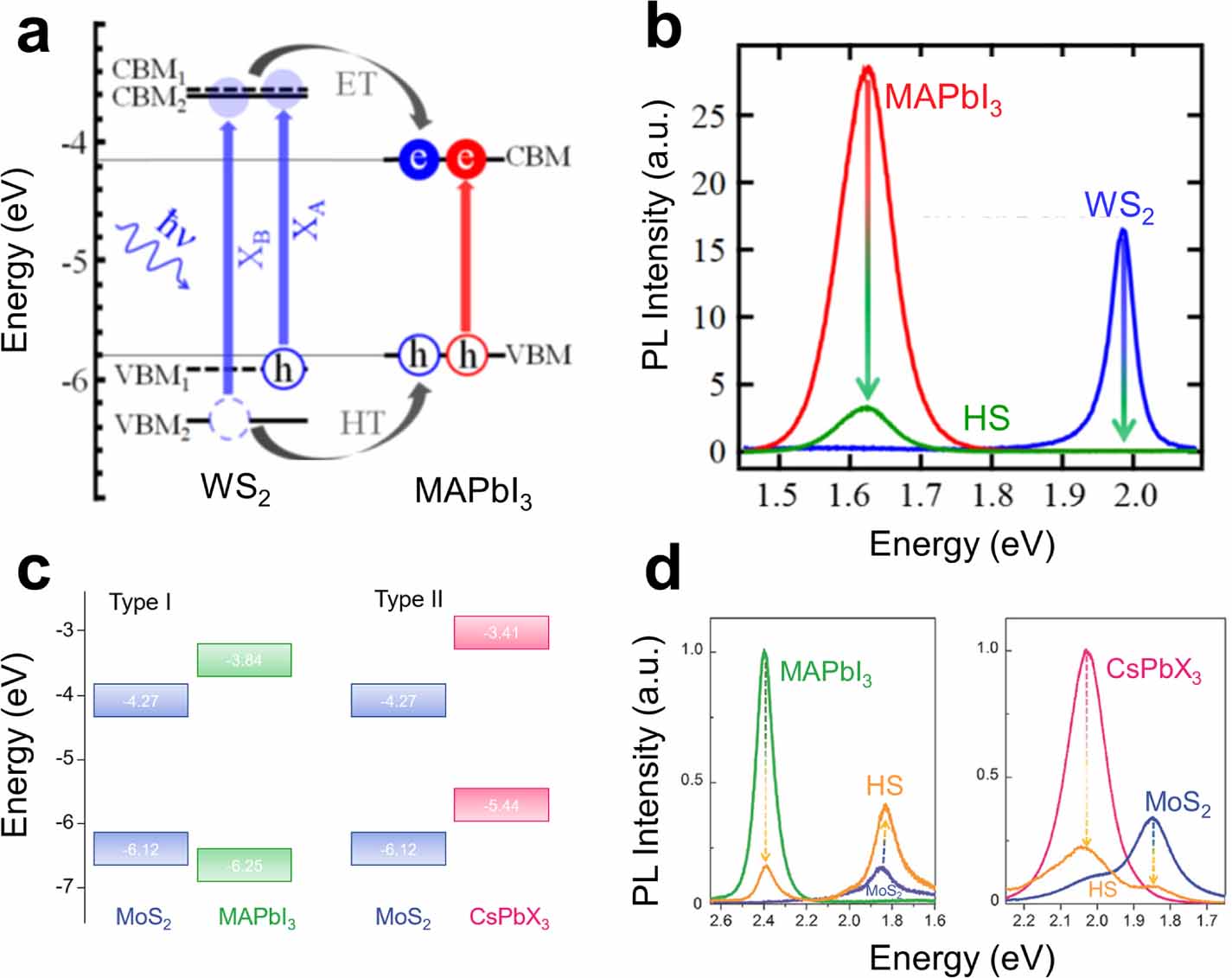
The first reports of TMDC/PM HSs date from 2016, where MAPbI3 thin films (10s–100s nm thick) were used as the perovskite layer [169–172]. While MoS2 had been used before as a hole-transport layer in organic solar cells, [173], in the TMDC/perovskite HS, it was used for the first time as an active absorbing layer, next to the perovskite layer. To tune the charge and energy transfer between the perovskite and TMDC, modulation of the band alignment between these two materials is essential. In this context, the work by Peng and co-workers is particularly interesting, who analysed charge transfer processes in a MoS2/MAPbI3 perovskite HS, where the MAPbI3 was 30 nm thick [171]. They experimentally analysed the excitonic states using pump-probe spectroscopy in a similar manner to what has been described in section 3.2. The work reported that the band edge alignment can be tuned by defect engineering: the type I heterojunction could be converted to a type II heterojunction using oxygen plasma treatment of MoS2. As a result of the band-alignment engineering, competitive charge transfer and energy transfer mechanisms could be varied. This work demonstrated highly efficient charge transfer in which 83% of the holes generated in the perovskite were transferred to the MoS2, on a timescale of 300 fs after photoexcitation. The fact that defects can play a strong role in the performance of these mixed HSs was explicitly investigated in another work, in which defects were passivated in a CVD-grown WSe2 monolayer through laser-induced oxidation. The photo-responsitivities of the resulting HS with a bulk-like film of MAPbI3 device with the treated monolayer were higher than the device with the untreated monolayer [172]. The more diverse band alignments in these mixed HSs are a main advantage over the typical TMDC/TMDC HSs, which generally form type II band alignments, as shown in figure 4. However, as the previous works show, the role of TMDC defects can not be neglected in the characterisation of the HSs.
In the following years, more works on the device performance of these HSs were published (see [176–181], for a selection, with various perovskite compositions and morphologies). While most of these works rely on the electronic charge- or energy transfer, it is worth pointing out at least one study that used the excellent emissive properties of a 37 nm thick layer of CsPbBr3 nanocrystals and subsequent radiative energy transfer to effectively boost the absorption of the underlying MoS2 layers [182]. Other works also went more deeply into the processes underlying the energy and charge transfer in the HSs. In this regard, the work from Bauer et al focused on a 100 nm thick film of MAPbI3 perovskites but with WS2 as the TMDC in the HS [174]. Akin to TMDC/TMDC HS analysis, they used microscopic ultra-fast pump-probe transient spectroscopy measurements combined with room-temperature PL spectroscopy, to determine the kinetics within the HS. This work presented a somewhat unusual finding: despite a type I band alignment, for which energy transfer and hence PL emission would be expected (figure 7(a)), the PL contributions from the individual constituents were quenched (figure 7(b)). As the PL was quenched in both materials, the authors concluded that energy transfer was not the dominant transfer mechanism. Rather, the strong binding energy of the excitons in the TMDCs and the small energy difference between the VBMs of the two materials limited the transfer of holes to the perovskites. While the holes from the B-exciton band could still transfer, the effective hole transfer rate was smaller than the electron transfer rate, for which both A-exciton band and B-exciton band electrons could contribute in the transfer from the TMDC to the perovskite. This resulted in an HS dominated by charge, not energy, transfer. This suggests that the peculiar spin–orbit physics of TMDCs has far-reaching effects for their functionality in HSs, opening up sophisticated ways of manipulating charge transfer by comparing A-exciton and B-exciton dissociation rates.
Figure 7. (a) Type I band alignment of a MAPbI3/MoS2 HS, MAPbI3 nanocrystals had an average diameter of 7. (b) Room-temperature PL spectra of the pristine layers and the HS of MAPbI3/MoS2. Despite a type I system, the PL quenching from the constituent emission bands suggests charge transfer occurs in this system. (a), (b) Reprinted with permission from [174]. Copyright (2018) American Chemical Society. (c) Band alignments of the compared structures in Wu's study, where the CsPbX3 had an average diameter of 15 nm. (d) The compared samples' pristine and HS room-temperature PL spectra. (c), (d) [175] John Wiley & Sons. © 2018 WILEY-VCH Verlag GmbH & Co. KGaA, Weinheim.
Download figure:
Standard image High-resolution imageExtending these band alignment considerations further, a HS of monolayer MoS2 and 40 nm thick CsPbBr3 nanosheets, with a type II alignment was reported [176], while another work showed a type I alignment between CsPbBr3 nanowires and monolayer MoS2 [183]. Similarly, a WS2 monolayer/CsPbBr3 180 nm thick microplate HS exhibited a type II alignment in one study [101], while in another study, WS2 with CsPbBr3 QDs (average size of 11 nm)—rather than sheets—resulted in a type I alignment [184]. In both examples, the calculated or measured bandgaps of the PMs did not change significantly; rather, the morphology and dimensionality of the perovskites seem to have caused the shift in band alignments. In terms of material dimensions, it was shown that the diffusion length of charges in a CsPbBr3 film is sufficiently long that perovskite films from 8 nm up to 200 nm thick can still efficiently transfer charges to TMDC monolayers [166, 167]. These examples indicate that the relative ease of solution processing of the perovskites combined with the spin–orbit split bands in the TMDCs allows a wide variety of band alignments to be engineered. As pointed out before, these spin–orbit split bands cause alignments that are neither precisely type I nor type II but create competing transfer processes [184].
Naturally, adjusting the perovskite bandgap by composition is a powerful way of tuning band-alignments. In 2018, a comparative study on the differences in the band alignments for inorganic and organic perovskite QDs, namely MAPbBr3 and CsPbBr I
I , with average diameters of 7 nm and 15 nm respectively, in MoS2 HSs was published [175]. Using ultra-violet photoelectron spectroscopy measurements, the work showed that organic MAPbBr3/MoS2 heterobilayers formed a type I band structure, while the inorganic CsPbBr
 I
I /MoS2 HS formed a type II structure (figure 7(c)). In line with the general PL quenching trend in type II structures, the CsPbBr
 I
I /MoS2 showed PL quenching in both layers, while for the type I HS, the PL intensity was quenched only for the MAPbBr3 QDs, but enhanced for the MoS2, highlighting the role of band alignment in the excitonic charge and energy transfer. The PL spectra obtained from this study are shown in figure 7(d). In addition to the PL and TRPL analyses, the authors also studied the optoelectronic performance of these HSs by separately incorporating them into photofield-effect transistors (PFETs). In both devices, the HSs were fabricated on top of back-gate SiO2/p-type Si substrates, and Au/Cr contacts were evaporated onto the substrates as the source and drain contacts. The performance of each system was analysed by current–voltage sweeps in the dark and under illumination. The measured photocurrent of the all-inorganic type II HS was more than four times that of the organic–inorganic type I HS. The superior optoelectronic properties of the all-inorganic HS was attributed to trapped long-lifetime carriers in the surface states or interface trap states, particularly arising from the MoS2 interface. The Cs-based system's ability to transfer photoexcited electrons while accumulating photogenerated holes resulted in a strong photogating effect, contributing to the overall enhanced optoelectronic performance. Conversely, both of the photogenerated electrons and holes were transferred to the MoS2 layer in the MA-based system, where they subsequently recombined; this ultimately led to a relatively poor performance in the organic–inorganic device. More generally, the authors argue in this work that the advantageous optoelectronic properties coupled with the higher overall stability of CsPbBr3 perovskite QDs may lead to more favourable TMDC/perovskite HS systems and devices in the future.
As shown by the Kovalenko group, the bandgaps of the all-inorganic perovskite nanocrystals change with the halide element, from around 3 eV in CsPbCl3 via 2.4 eV for CsPbBr3 to 1.8 eV for CsPbI3 [165]. This change in bandgaps is accompanied by a change in band energies [88], and it will be interesting to see if the facile change in halides can induce a change from a type II to a type I HS. However, no systematic experimental study exists yet on this halide-dependent band alignment in an HS with TMDCs. Clearly, the facile exchange of cations and anions in semiconducting PMs promises a wealth of tunability for HSs in the near future.
Finally, further opportunities for interfacial engineering in TMDCs/perovskite HSs arise through the surface chemistry of the perovskites, or by inserting spacer layers between the two materials. Using room-temperature, TRPL spectroscopy, Liu et al showed that the introduction of hBN spacer layers between all-inorganic perovskite nanocrystals, with average sizes of 8.5 nm and monolayer MoS2 altered the PL lifetime of the perovskite nanocrystals, with shorter lifetimes for thinner spacers [80]. They showed that the charge transfer rates can be effectively modulated by introducing hBN flakes of up to 7 nm thick. Using ligand engineering in the same HS, albeit with slightly larger nanocrystals of around 15 nm, interfacial charge transfer was enhanced by removing as much of the nanocrystal ligands as possible without compromising the stability of the perovskite nanocrystals [185]. With this treatment they improved the photo-responsitivity of their photodetector devices by a factor of 15. Another approach to ligand engineering exists for quantum-confined nanocrystals, where the choice of surface ligands can affect the band alignments, without changing the bandgap. This has been shown before for QD HSs [186], but to our knowledge, not yet for mixed TMDC–perovskite HSs.
The above examples demonstrate that elemental composition, dimensionality, morphology, defects, layer distances and surface chemistries of a TMDC/perovskite HS can all alter the band alignment of the HS, which in turn, determines the extent of charge or energy transfer between the layers. As a consequence, the simple band alignment picture is not always indicative of charge or energy transfer processes, as can be seen by comparing the panels of figure 7. Rather, a combination of experimental methods such as (time-resolved) PL and TA spectroscopy is required to determine the charge kinetics in TMDC/perovskite HSs.
Therefore, the same combination of techniques that already provided insight into the charge dynamics of TMDC/TMDC HSs is useful in elucidating the carrier dynamics in the TMDC/perovskite HSs, as will be discussed in the following sections.
4.3. Signatures of charge transfer
Steady-state PL spectroscopy, particularly PL spectroscopy at low temperatures, is a convenient technique to optically characterise the TMDC/perovskite HSs. In Wu's comparative analysis, the PL quenching in the CsPbX3/MoS2 HS indicated full energy transfer, while the PL quenching of the organic perovskite along with the PL enhancement of MoS2 indicated charge transfer [175]. This argument is generally applied in most TMDC/perovskite reports [101, 184, 187].
Besides that, low-temperature PL measurements can provide insights into the kinetics of the biexcitons and charged excitons within a TMDC/perovskite HS, which otherwise would not be observed. For example, one study reported the PL of a WS2/microplate CsPbBr3 structure and its pristine components at 3.3 K to resolve the excitonic emission bands [101]. As the density of the biexcitons varies quadratically with the number of excitons in the pristine TMDC monolayer, small fluctuations in the exciton density, which may be undetectable in many PL systems, can be detected from changes in the biexciton emission (figure 8). Additionally, since the binding energies of trions and biexcitons are lower than those of neutral excitons, the driving force for charge separation at the interface will be more effective for these exciton complexes. At low temperatures, the authors observed full quenching of the biexciton emission in the HS compared to the monolayer, indicating that charge transfer occurred within the sample.

Figure 8. Low-temperature PL spectra of the WS2 pristine sample and the WS2/CsPbBr3 HS. The CsPbBr3 consists of 180 nm thick microplates. Note the emission differences from the neutral exciton (X), the charged exciton ( ) and the biexciton between the spectra. Reproduced from [101], with permission from Springer Nature.
Download figure:
Standard image High-resolution imageAdhikari et al further studied the excitonic room-temperature PL spectra of a CVD-grown monolayer MoS2 and 11 nm sized CsPbBr3 nanocrystals HS and noted that each of the neutral A and B excitons and the negatively charged A− exciton red-shifted in the HS [188]. Their argument was further strengthened by showing more dominant trion emission, independent of laser power, and related shifts and power dependence in TA measurements. Furthermore, by constructing gated devices with and without the QDs, the work also found a downshift in the threshold voltage in the HS compared to the pristine device. Both indicate that the MoS2 layer's electron concentration was higher in the hybrid than in the pristine sample. In turn, this implied charge transfer had occurred in the HS, with electrons transferred from the QDs to the MoS2. Overall, this study highlights the difficulty of characterising charge transfer by exciton lines, as both the exciton binding energy as well as the electronic bandgap can shift with the influx of charges.
Before we continue towards alternative signatures of energy transfer, we briefly exemplify a lead-free system, namely the evaporated CsSnBr3/WS2 (grown by CVD) HS as recently fabricated and characterised in the work of Mu et al [189] The key novel concepts summarised from this work are two-fold: first, as it has been argued that toxicity of lead will limit the extent of future applications for any perovskite optoelectronic device, a substitution of lead by another element such as tin is necessary. Second, contrary to the majority of published works using mostly solution-processed methods such as mechanical exfoliation or vacuum deposition to prepare the perovskite, in this study, precise tuning of the perovskite thickness (varying between 10 nm and 70 nm) was achieved using thermal evaporation. The optical properties were characterised using UV–VIS absorption spectroscopy, steady-state PL and TRPL. Using UV–VIS measurements supplemented with XPS, the HS was found to exhibit type-II band alignment. The observed PL quenching in this system together with the differences in TRPL lifetime was attributed to charge carrier transfer across the system. This work by Guo et al is a pioneer study on the use of lead-free perovskites in TMDC-based HSs. Their findings are naturally not as encompassing as those from the multitude of studies done on lead-based perovskite HSs. However, their study presents an important step towards sustainable implementation of TMDC/PM HSs and it will be interesting to see future work going deeper into the comparison of lead-based and lead-free perovskite/TMDC HSs.
4.4. Exciton- and energy transfer
PL lifetimes can also yield insight into the possible formation of IEs and whether charge or energy transfer occurs in a TMDC/perovskite HS. For example, room-temperature TRPL and fluorescence lifetime imaging microscopy measurements of organic–inorganic heterostructures found that the average PL lifetime of the CsPbBr I
I QDs was 16.7 ns, which reduced to 6.2 ns in the MoS2/ CsPbBr
 I
I HS, while the average PL lifetime of MAPbBr3 reduced from 11.2 ns in the pristine sample to 2.9 ns in the HS [175]. This reduction was attributed to the charge extraction kinetics of the HS.
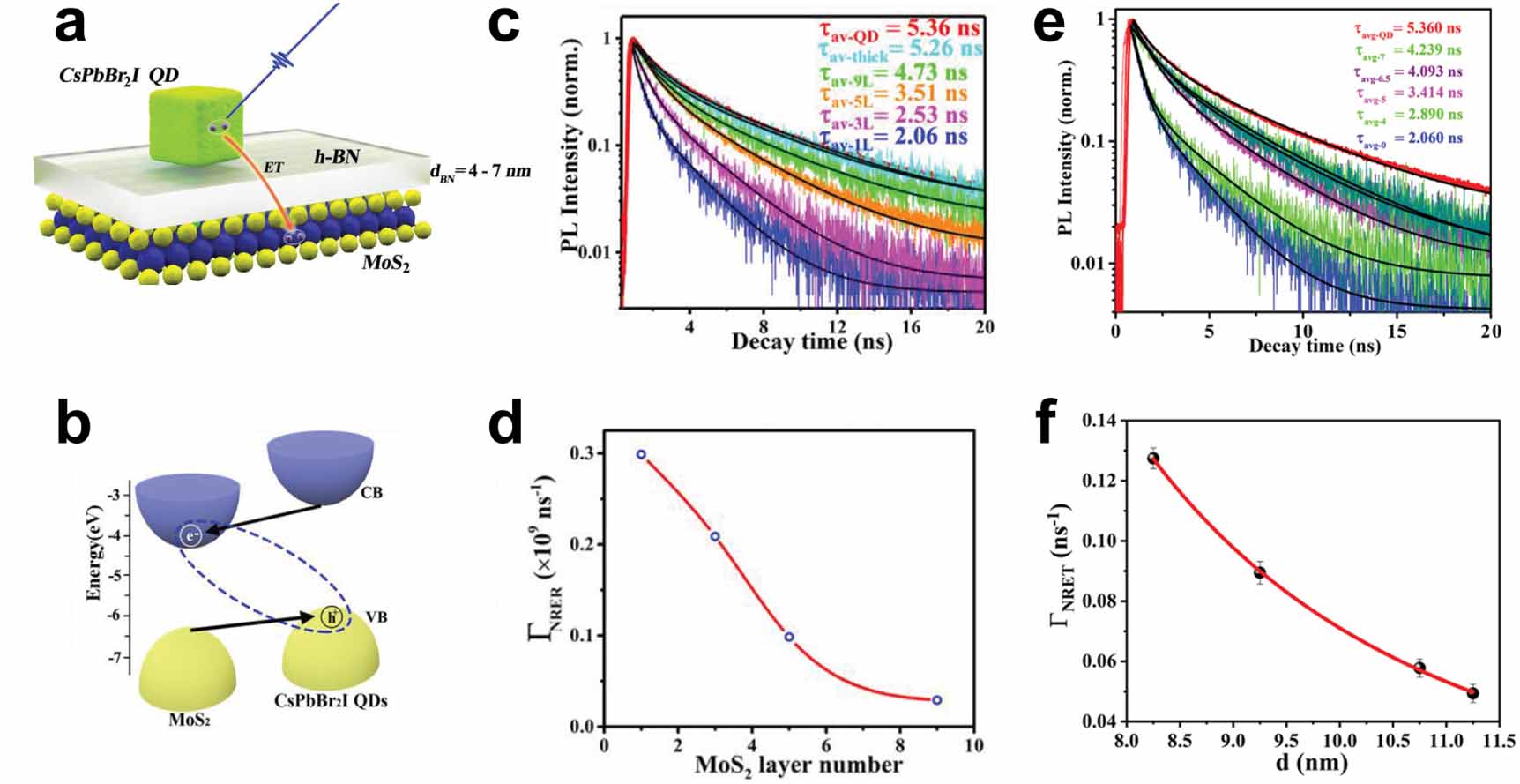
Further insights into interfacial dynamics can be obtained by varying the interfacial width, and evaluating its effect on the charge transfer dynamics. By either decreasing the thickness of MoS2 or removing insulating hBN layers between the materials [80], the PL lifetime of the perovskite QDs decreases (figure 9), indicating the presence of an additional relaxation channel. Panel (c) of figure 9 shows the TRPL data for varying MoS2 layer thickness, and panel (d) the extracted thickness-dependent relaxation rate, which saturates for thicknesses of around 10 MoS2 layers, approaching the value of the isolated QDs. Panels (e) and (f) reveal a similar behaviour for the thickness of an hBN spacer layer between the QDs and an MoS2 monolayer. This decrease of the QD PL lifetime suggests the emergence of additional non-radiative relaxation channels that become activated for lower energy barriers or when the band-alignment of the two compounds becomes more favourable due to thin MoS2 as opposed to thicker MoS2. This thickness-dependent PL lifetime thus points to the presence of charge transfer across the HS.

Figure 9. (a) Schematic and (b) band alignment of the monolayer MoS2 and 8.5 nm sized CsPbBr2I nanocrystals HS studied by Luo and co-workers. (c) Room-temperature TRPL spectra of the HS with additional MoS2 layers. (d) The corresponding non-radiative relaxation rate as a function of the increasing number of MoS2 layers. (e) TRPL spectra of the HS with increasing hBN spacer thickness. (f) The corresponding non-radiative relaxation rate as a function of the hBN spacer thickness. [80] John Wiley & Sons. © 2019 WILEY-VCH Verlag GmbH & Co. KGaA, Weinheim.
Download figure:
Standard image High-resolution image4.5. Signs of interlayer excitons?
Ultrafast spectroscopic characterisation thus presents a powerful tool to study the kinetics and determine rates of charge- and energy transfer in TMDC/perovskite HSs. It is therefore interesting to ask whether similar to TMDC/TMDC HSs, there have been signs of spatially separated IEs in mixed HSs as well. The studies towards this topic are few in the mixed TMDC/PM HS. Nevertheless, an interesting study was presented by Li et al, who performed a full analysis of the charge dynamics across a WS2/CsPbBr3 QD HS using a combination of femtosecond TA spectroscopy and room-temperature steady-state PL [184]. The TA signal showed photobleaching (PB) proportional to the exciton fluence and photoabsorption (PA) due to biexcitons and other pump-induced absorbing states, see figure 10(a). The quenching of the PB signal suggests that few excitons remain in the QDs after excitation. Additionally, the PB signal of the A-exciton resonance was enhanced, suggesting that the excitons generated in the perovskite were immediately transferred to the TMDC. To pin down the competitive processes behind the PB and PA features, 'zero-points' (ZP) were defined at probe wavelength positions where the photo-induced absorption vanished (vanishing ΔA in figures 10(b) and (c). In the HS, these ZPs shift over time towards an increased PA feature, indicating the formation of a built-in electric field due to IEs across the HS, which in turn altered the resonances of the excitons in the WS2 layer. This concept had previously been described by He and co-workers for a WS2/graphene HS [190], and here could be developed into a full model of the recombination dynamics and fitted to the TA signal for fast and slow recombination processes as depicted in figure 10(d).
Figure 10. (a) Transient absorption spectroscopy with photobleaching (PB) and photo-induced absorption (PA) signals labelled for the monolayer WS2, 11 nm sized-CsPbBr3 nanocrystals pristine samples and the WS2/CsPbBr3 HS. PB1 (PB2) refers to the PB signals of the A (B) excitons. (b) TA signal of the A exciton resonance of the WS2 structure. (c) TA signal of the A exciton resonance of the HS. Note the evolution of the ZP and the enhanced PA effect in the HS compared to the pristine sample. (d) Kinetic model of the ultra-fast charge processes of the HS. Reproduced from [184] with permission from the Royal Society of Chemistry.
Download figure:
Standard image High-resolution image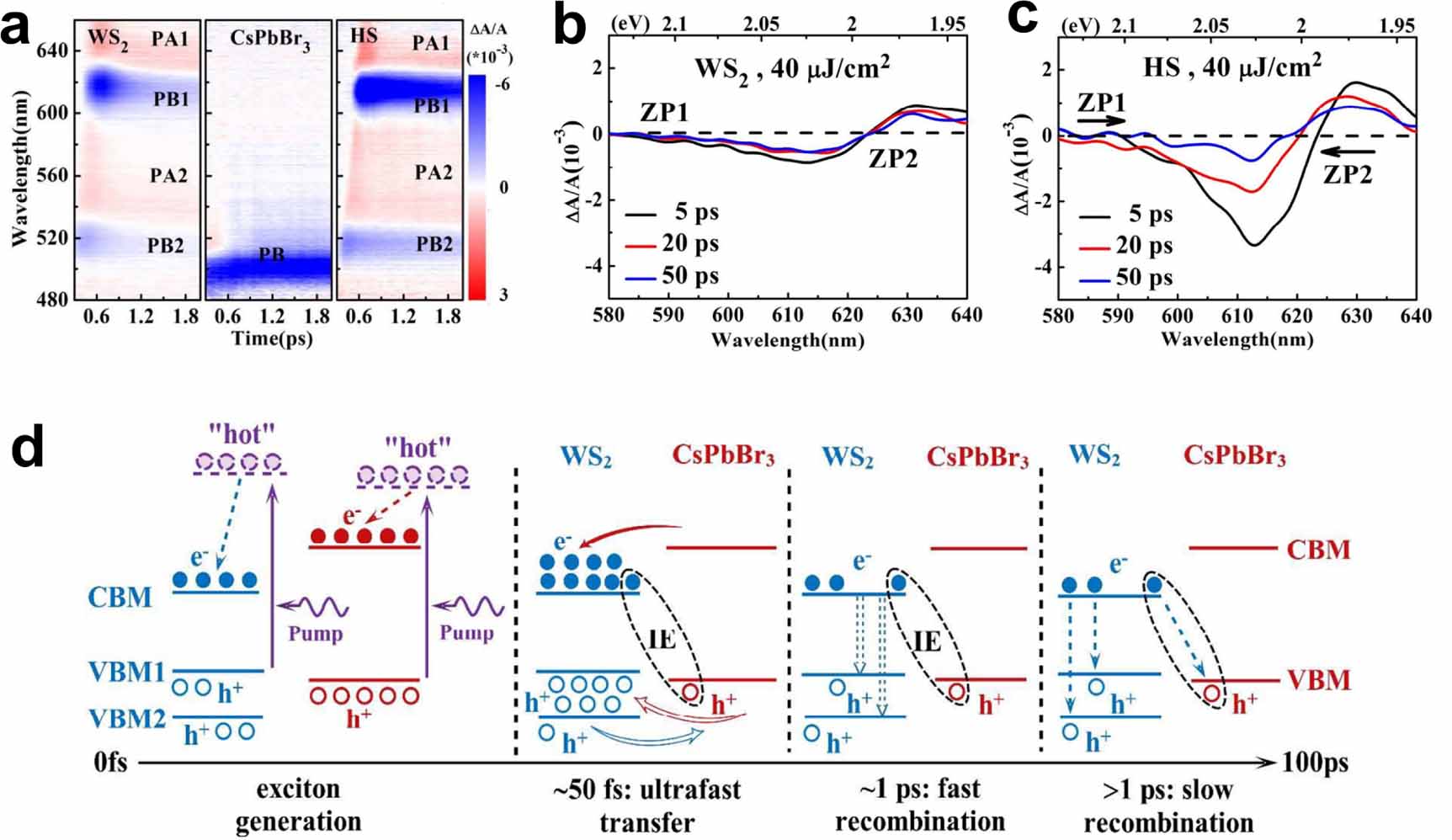
4.6. Further considerations
In addition to the above examples of thin films or QDs of lead halide perovskites with ABX3 structure, 2D Ruddleston–Popper perovskites, with a structure of A B
B X
X are also widely employed as one of the layers in TMDC/perovskite HS [187, 191–193]. As an example, excitonic energy transfer has been observed in the quasi-hybrid perovskite C6H5C2H4NH3 (PEPI)/WS2 HS, with the PEPI being around 100 nm thick and monolayer WS2 [187]. Experimental evidence for the energy transfer was presented using PL, PLE and reflectance spectroscopy techniques. In the PLE measurements performed at 110 K, the authors observed that the A exciton PL from WS2 is enhanced at the excitation energy corresponding to the exciton of PEPI, indicating energy transfer between the two compounds had occurred. Overall, while many initial works have been performed on these mixed HSs, important details of the fundamental processes are yet to be uncovered. For example, many tuning parameters have been discussed above, but it is not always clear how these tuning parameters affect the time dynamics of charge transfer. To gain further insight, the optical experimental methods described above should be supplemented by further optical measurements such as reflectance spectroscopy, and other physical characterisation methods such as x-ray diffraction, TEM, and atomic force microscopy, and by theoretical analyses. In this regard, a theoretical study using time-dependent DFT points to yet another factor in band alignments [194]. The authors found that the exact crystal facet of CsPbBr3 nanocrystals exposed to the TMDC can alter the band alignment and suggested that this can be an alternative explanation for mixed band-alignment, besides the spin–orbit splitting mechanism proposed by Bauer et al [174]. This interpretation is still discussed in the follow-up theoretical work by Liao et al, who found a type II alignment for both crystal facets in the same system [195]. Subsequently, Xu et al stressed that the different crystal facets of CsPbBr3 do result in different band alignment types with MoS2, as long as the SOC is included to describe the properties of the perovskite [196]. Similar work has been undertaken on the CsPbBr3/MoSe2 system, where both perovskite facets show a type II alignment with the TMDC [197]. Finally, also in the case of the CsPbI3/MoS2 and CsPbI3/WS2 systems, the alignment turns out to be of type II, independent of the perovskite facet exposed to the TMDC. This shows that for some specific combinations, such as CsPbBr3/MoS2, the band alignment is so close between type I and type II that the specifics of crystal facets, and SOC start to become important [198]. It will be interesting to see how these effects, and the aforementioned tuning parameters, overlap in less-than-ideal macroscopic samples and practical situations.
Before we address the alternative processes that may be occurring in TMDC/TMDC and TMDC/PM HSs, we summarise the key experimental reports that we have previously discussed regarding TMDC/PM HSs in table 1.
Table 1. Summary of the experimental works discussed in this literature review which characterise various TMDC/PM heterostructure materials using various key optical methods. These tabulated works also explicitly identify the heterostructure type and describe evidence for either charge transfer, energy transfer, or both. Abbreviations: BA = butylamine, N.D. = not described, Abs. = UV–VIS absorption spectroscopy, TRPL = time-resolved photoluminescence spectroscopy, TAS = transient absorption spectroscopy, DRS = differential reflection spectroscopy.
| TMDC/perovskite | Perovskite type | HS type | Transfer type | Key optical techniques | Year | Reference |
|---|---|---|---|---|---|---|
| WS2/CsPbBr3 | Microplates | Type II | Charge | Abs., PL, Raman | 2018 | [101] |
| MoSe2/CsPbBr3 | Nanocrystals | Type I | Energy | Abs., PL, TRPL | 2022 | [153] |
| WSe2/CsPbBr3 | Thin film | Type I | Energy | Abs., PL, TAS | 2021 | [166] |
| MoS2/CsPbBr3 | Thin film | Type II | Charge | Abs., PL, TAS, TRPL | 2022 | [167] |
| WS2/CsPbBr3 | Thin film | Type II | Charge | Abs., PL, TAS, TRPL | 2022 | [167] |
| MoS2/MAPbI3 | Thin film | Type II | Charge | PL, TAS, Abs., Raman | 2016 | [171] |
| WS2/MAPbI3 | Thin Film | Type I | Charge | Abs., PL, TAS, DRS | 2018 | [174] |
MoS2/CsPbBr I I
| Quantum dots | Type II | Charge | Raman, PL, TRPL | 2018 | [175] |
| MoS2/MAPbBr3 | Quantum dots | Type I | Energy | Raman, PL, TRPL | 2018 | [175] |
| MoS2/CsPbBr3 | Nanosheets | Type II | Charge | Abs., PL, TRPL | 2018 | [176] |
| WS2/CsPbI3 | Nanocrystals | Type II | Charge | Abs., PL, TRPL, Raman | 2023 | [180] |
MoS2/CsPbI Br Br
| Quantum dots | Type II | Charge | Raman, Abs., PL, TRPL | 2018 | [181] |
| MoS2/Cs0.85FA0.15PbBr3 | Quantum dots | N.D. | Charge | Raman, Abs., PL | 2022 | [182] |
| MoS2/CsPbBr3 | Nanowire | Type I | Energy | Raman, PL, TRPL, TAS | 2018 | [183] |
| WSe2/CsPbBr3 | Nanowire | Type II | Charge | Raman, PL, TRPL, TAS | 2018 | [183] |
| WS2/CsPbBr3 | Quantum dots | Hybrid I/II | Charge | TAS, PL, Raman | 2018 | [184] |
MoS2/CsPbI Br Br
| Quantum dots | Type II | Charge | Abs., PL, TRPL, Raman | 2019 | [185] |
| WS2/(C6H5C2H4NH3)2PbI4 | Quasi-2D flakes | Type II | Energy | DRS, PL, PLE, Raman | 2020 | [187] |
| MoS2/CsPbBr3 | Quantum dots | Type II | Charge | Abs., PL, TAS, Raman, TRPL | 2020 | [188] |
| WS2/CsSnBr3 | Thin Film | Type II | Charge | Raman, Abs., PL, TRPL | 2023 | [189] |
WSe2/(C4H9NH3) PbI4 PbI4
| 2D Microplates | Type II | Charge | PL, Raman | 2020 | [191] |
| WS2/(C6H5C2H4NH3)2PbI4 | 2D single crystals | Type II | Charge | DRS, PL | 2020 | [192] |
| WS2/(BA)2(MA)3Pb4I13 | 2D bulk crystals | Type I | Charge | Raman, PL, PLE, TRPL | 2019 | [193] |
5. Alternative processes
While the aforementioned features such as the additional low-energy, long-lived PL and quenching of the excitonic peaks of both HS components have been attributed to charge transfer between the materials and the formation of the IE, alternative processes are also imaginable. In principle, the additional PL emission peaks, PL quenching, prolonged lifetimes and even unusual TA signals can all be attributed to entirely different processes. For example, the formation of radiative defect states in the HS can result in a change in the average lifetime and can be recorded as a low-energy PL signal. It is therefore crucial to differentiate such spectroscopic peculiarities from IE formation and recombination processes in TMDC HSs.
In fact, TMDC monolayers can have an array of intrinsic point defects, grain boundaries, surface defects, vacancies and adatoms; these defects and their densities can vary across different materials and different fabrication procedures [64, 119, 120]. These intrinsic defects can alter the PL, band gaps and recombination lifetimes, where the defect-assisted recombination typically triggers Auger recombination in such monolayers [63, 199, 200]. Furthermore, the substrate can contribute to the variation of the monolayers' and HSs' optical properties. For example, PL quenching has been shown to occur when TMDC monolayers were grown on graphene compared to their PL emission when fabricated on rigid substrates [201–203]. Furthermore, PL quenching may simply be a result of less overall irradiation of the sample when in an HS configuration compared to a pristine sample. Optical spectroscopic tools, as described above, along with scanning electron microscopy (SEM), TEM, XPS, secondary-ion mass spectrometry (SIMS) and other physical characterisation techniques, combined with density functional theory (DTF) and electron energy-loss spectroscopy (EELs) calculations provide a means to analyse such defects and differentiate between different mechanisms [82, 83].
Some, albeit not all, works that analyse TMDC/TMDC and TMDC/perovskite HS also consider alternative mechanisms that could explain their spectroscopic results. For example, Bauer and co-workers considered that the PL quenching of WS2 in their TMDC/perovskite HS could simply be due to the excitation from the laser not reaching the WS2, due to their MAPbI3 layer being 100 nm thick [174]. They addressed this consideration by fabricating the HS on a transparent (sapphire) substrate and illuminating the structure from the backside. In both cases, WS2 PL was quenched, showing that reduced absorption in the WS2 layer was not the reason for PL quenching.
Rivera and co-workers partially omitted the possibility of defect states formed in MoSe2/WSe2 HS by fabricating homostructures using the TMDC monolayers and finding that the signature IE signals in the HS could not be reproduced in the homostructures [14].
Similarly, Chen and co-workers considered that the low-energy PL peak in the 2D perovskite/TMDC HS could arise from laser-induced defect states. To exclude this possibility, temperature-, power- and excitation-energy-dependent steady-state PL measurements were conducted on the isolated perovskite, which would have been expected to thermally degrade and reproduce the broadened peak observed in the HS; yet, this peak was not observed in isolation, indicating that thermal degradation does not occur. Furthermore, to verify that the excitonic emission quenching originated from charge transfer, they inserted an insulating 6 nm thick hBN layer between the TMDC and perovskite layers and showed that the excitonic emission of the monolayers was not quenched, as no charge was transferred. They stacked the layers in an inverse order to show that the exciton emission had been present regardless of stacking sequence and varied the TMDC employed to show that IEs were formed in similar type II band alignment configurations, verifying that the IE signals were reproducible under different configurations [191].
While the above-mentioned works refute the formation of defect states and possible changes in the HS, other works do find clear signatures of them. Concerning the latter, the work of Mohite and Atwater on a 7.5 nm thick 2D perovskite and a bilayer WS2 HS is noteworthy [193]. They observed broadened PL peaks at low temperatures for different 2D perovskite/WS2 HSs which were directly attributed to emissive defect states, as these peaks were not present at higher temperatures. The defect states in both the TMDC bilayer and the HS were further confirmed using differential reflection spectroscopy. Wu and co-workers fabricated PFETs from the perovskite QD/TMDC HS and attributed the measured photo-gating effect to trapped long-lifetime carriers in the surface states or interface trap states [175]. This effect was also observed in TMDC monolayers [204, 205]. Additional reports also have shown that PL emission observed can be directly from defect states of the bilayers of samples [193, 206–208]. These experiments verify that indeed such HSs can exhibit surface defect states that can interfere with the optoelectronic characteristics, making a thorough characterisation using complementary optical and structural analysis indispensable.
6. Conclusions
TMDC monolayers are intriguing materials due to their enhanced optical properties and strong excitonic effects. Despite intense studies, this class of semiconducting materials still holds promise for exciting developments, especially towards the optoelectronic properties of less well-known compounds such as the Re, Zr, Hf dichalcogenides, alloys and Janus monolayers. Even for the more well-known Mo and W dichalcogenides, a whole zoo of materials is left to explore once they are combined in HSs. Specifically, the stacking-angle dependence on their optoelectronic properties is an active field of research. The formation of IEs is especially exciting because these long-lived states have a more diverse set of tuning parameters than the excitons formed within the layers. In this regard, it will be of interest to investigate the interplay between electron- and hole wavefunction overlaps and the momentum-indirect nature of IE transitions. The latter aspect is especially intriguing as it could point to an as-of-yet under-investigated tuning parameter. In this regard, the common molybdenum- and tungsten-based TMDC HSs all show similar behaviour where the individual electron and holes seem to reside in different valleys of momentum space. However, combinations with the aforementioned Re and other transition-metal materials offer fresh alternatives and it will be intriguing to study the effects of different k-space transitions in HSs of these new compounds.
Further degrees of freedom exist in the emerging field of mixed HSs, which we have reviewed here with a focus on TMDC/perovskite HSs. Since the perovskites are easily tunable by composition, dimensionality and surface chemistry, the possible combinations, and tuning parameters, for HSs with TMDC monolayers are vast. We believe that, while all works discussed here are interesting on their own, systematic investigations of the interplay of all these factors are still missing. Because of the complexity of these structures, future works must adapt and expand on the current spectroscopic techniques as single measurements alone are insufficient for reaching conclusions. Furthermore, optical spectroscopic characterisation methods should be combined with physical and chemical analyses, along with theoretical calculations and interpretations, to attain a full dynamical model of each potential HS. It is tempting to neglect alternative defect state processes and other mechanisms when interpreting the measured optical features. These alternative considerations need to be included in future works on TMDC heterobilayer analysis, to achieve a full picture of the processes within the HS.
The 2D TMDC HS research field is still relatively young, and the progress in the understanding of IEs and the overall charge dynamics in TMDC HSs is impressive. Experimental optical characterisation methods have been key in driving these developments and continue to do so. One thing completely neglected in this review is the possibility of stacking more than two layers, which widens the scope of combinations even further. Overall, the TMDC HSs are full of possibilities, and it will be interesting to see future device applications come out of this highly interesting field.
Acknowledgments
This research received funding from the Netherlands Organisation for Scientific Research (NWO) in the framework of the Materials for Sustainability Programme (MAT4SUS Project No. 739.017.011).
Data availability statement
No new data were created or analysed in this study.