
Abstract
We review theoretical and experimental highlights in transport in two-dimensional topological materials over the last five years. Topological materials comprise topological insulators, Weyl semimetals and topological superconductors. This review focuses on key developments in the understanding of transport phenomena involving surfaces and interfaces of two-dimensional topological materials that have not been covered elsewhere. The review is structured around the following general topics: (i) topological insulators are finding applications in magnetic devices, while controversy continues to surround Hall transport in doped samples and the general issue of topological protection; (ii) state-of-the-art experiments on transition metal dichalcogenides have revealed new valley-dependent electrical and optical phenomena which have spin-dependent counterparts in topological insulators; (iii) in Weyl semimetals the manifestations of Fermi arcs in transport are actively investigated as well as controversial; (iv) a new and growing field centres on the non-linear electrical and optical responses of topological materials, where fundamental questions emerge about the interplay of the Berry curvature and disorder scattering; and (v) topological superconductor research is dominated by the quest for chiral superconductivity, Majorana fermions and topological quantum computing. Prospects for future research in this vast field are outlined in the closing section.
Export citation and abstract BibTeX RIS

Original content from this work may be used under the terms of the Creative Commons Attribution 3.0 licence. Any further distribution of this work must maintain attribution to the author(s) and the title of the work, journal citation and DOI.
1. Introduction
The new millennium has witnessed the seemingly inexorable rise of topological phenomena, culminating in the 2016 Nobel Prize in Physics. The term topological materials encompasses a broad range of structures that exhibit phases characterised by a topological invariant [1, 2] that remains unchanged by deformations in the system Hamiltonian. This can be the Z2 invariant or the Chern number, or the discussion can be phrased more generically in terms of the Berry curvature, whose integral over the Brillouin zone yields the Chern number. Topological materials include topological insulators (TI) [3, 4], Weyl and Dirac semimetals (WSM, DSM) [5], and topological superconductors (TSC) [3]. The distinction is not always clear cut, since some categories overlap. For example, certain transition metal dichalcogenides (TMD) can become topological insulators under appropriate circumstances [6, 7], while others, such as WTe2, can be Weyl semimetals. An enlightening and general topological classification of band structures has been given in [8].
2D topological materials offer opportunities that did not exist previously. To begin with, in the structures we will consider the electron gas is on the surface and is directly accessible, unlike semiconductor heterostructures, where it is buried. This facilitates excellent electrostatic control over the conduction in the 2D channel, which enables transistor applications, as well as accessibility to light for optical applications. Next, many topological materials exhibit very strong spin–orbit coupling, which, under appropriate conditions, may yield dissipationless edge state conduction without large magnetic fields, leading to potential transistor applications through the quantum spin and anomalous Hall effects. Furthermore, in TI spin–orbit torques have taken off spectacularly, especially since the low mobilities of TIs are not a concern as long as large currents can be achieved by increasing the electron density, as was done in Bi2Te3 [9]. A good example of the manifold uses of topological materials is provided by the TMD WSe2, which has an extraordinarily large spin–orbit coupling, a wide direct band gap, and especially a strong anisotropic lifting of the valley degeneracy in a magnetic field, which makes it ideal for accessing the valley degree of freedom. Indeed, one major advantages of TMDs is that they can be made atomically thin and have a direct band gap, making them ideal for optical emitters and detectors. They display strong excitonic effects and piezoelectricity [10]. Topological superconductivity has also witnessed impressive growth, with exciting developments in achieving novel effects such as chiral superconductivity, Majorana edge modes [11], the fractional Josephson effect and unconventional Cooper pairing.
In direct analogy with the rise of graphene, topological materials have matured into a topological zoo with broad applications across different fields. In this review we emphasise this breadth of interest while bringing out conceptual unifying features such as spin- and pseudospin-charge coupling, the Berry curvature and inter-band effects and their interplay with disorder, and Cooper pairing in topological materials. We concentrate on the most actively researched two-dimensional transport phenomena in TI, WSM Fermi arcs, TMD, and TSC that have not been discussed in detail elsewhere—indeed, we are not aware of any recent review devoted exclusively to transport. With this in mind we dwell on salient issues that have preoccupied researchers for approximately the past five years: the relationship between spin-momentum locking and spin–orbit torques, the issue of topological protection and prospects for achieving dissipationless transport, the analogy between the anomalous Hall and valley Hall effects, the robustness of Fermi arcs as manifested in transport, the rise of non-linear phenomena and recent developments involving Majorana fermions. We include highlights from optical studies, since transport and optical responses are intertwined, and are broadly described by linear response theory (and beyond). They must frequently be considered on the same footing, for example in determining the non-linear optical response, in which a DC shift or rectification current is also generated.
The bulk of the review focuses on surface states. We first present a conceptual overview of the subject, followed by a review of transport in non-superconducting topological materials. The theoretical component of this section centres on insights obtained from linear-response theory and extensions thereof, while the experimental component reviews progress in the laboratory. After introducing the main model Hamiltonians and outlining the concepts behind linear response and inter-band coherence, we discuss transport in topological insulators, with particular emphasis on weak localisation and anti-localisation, the quantum Hall effect, spin–orbit torques and their relation to the current-induced spin polarisation and spin-Hall transport, magnetoresistance and the anomalous Hall effect. We pay special attention to the continuing controversy surrounding topological protection and transport by the edge states of topological insulators. The anomalous Hall effect has an extension in transition metal dichalcogenides, which have multiple valleys, and exhibit a valley-Hall effect, which is reviewed next. In Weyl semimetals we focus on Fermi arcs and their manifestation in transport. We discuss the non-linear electrical response, a burgeoning field with important unanswered theoretical questions and potential applications in photovoltaics and solar energy. The latter half of the review is devoted to the latest theoretical and experimental developments in chiral superconductivity, Majorana edge modes and related phenomena in topological superconductivity.
2. Background
Here we attempt a conceptual summary of topological materials and Weyl–Dirac physics in a condensed matter context, and of transport phenomena in these materials. Our aim is to provide basic explanations for commonly encountered terms in the literature.
2.1. Berry curvature
The forces that affect electron transport in a topological system originate from the interaction between the spin and orbital degrees of freedom of the electron. At the microscopic level these forces have a detailed description and they shape the band structure of a crystal. Once we know the band structure, we can find the macroscopic response of the material by using Bloch waves and their scattering properties. So what is the overall effect of the microscopic spin–orbit mechanism on the motion of electrons in a crystal?
To answer this question, we simply write down the equation of motion for a wave-packet of electrons moving in the lattice. Such a packet has a finite width about its centre of mass and an average wave momentum. The Lorentz force due to the external electromagnetic field steers this packet around the crystal, while the wave momentum evolves in the Brillouin zone (BZ) according to

In a non-trivial multi-band system, the energy and thus the Hamiltonian of the electron depend not only on the average position of the electron in the crystal but also its wave momentum in the BZ. We can regard this as a situation where the Hamiltonian is adiabatically changed via a parameter, in this case the momentum.
In quantum mechanics, the wave function acquires a dynamical phase factor due to energetic oscillation of the eigenstates. Asside from this, Berry studied the effect of a slowly changing Hamiltonian and found that an additional geometric (Berry) phase is accumulated [12]. In addition to the dynamical phase  , where
  is the energy, the geometric phase must be taken into account in calculating the velocity of the wave packet

through the Berry curvature term  [13]. With this term the equations for the velocity and acceleration look similar, where the Berry curvature plays the role of a gauge field defined in momentum space, which is the BZ of a crystal. The gauge field is simply a device to account for the local phases that arise from the band structure. The similarity with a magnetic field is not surprising, after all, what is an electromagnetic field? It is a manifestation of wave functions acquiring different phases at every point in space-time. Now the wave function also acquires local phases in momentum space, which manifest themselves in the Berry connection

where u is the periodic part of the Bloch wave. The relationship between the Berry curvature and Berry connection is

analogous to the magnetic vector potential and magnetic field. Therefore,  has a gauge freedom arising from the choice of basis, whereas the curvature
  is a gauge invariant physically meaningful quantity.
2.2. Berry curvature and Chern invariant
At low temperatures, the electrons in a material occupy the lowest energy states and, due to the exclusion principle, form a Fermi sea. To obtain the value of a physical quantity, we fist calculate it for a given energy and sum over all the energies in the Fermi sea. Given the equations of motion, if we assume that the applied fields are small, this sum must contain functions of the dispersion relation  , Berry curvature
  and their derivatives. In an insulator, this means integrating over the completely filled band over the BZ. The simplest such observable is the integral of the Berry curvature over the BZ, called the Chern number.

It turns out this is a topological invariant, meaning that perturbations to the bands do not change it unless the band structure is reordered and band crossing points are created or destroyed, in which case it changes by an integer. Now we show that a 2 band insulator has a finite transverse conductivity if the Chern number is non-zero.
2.3. Chern insulator
If we have a two dimensional crystal, in the presence of spin–orbit coupling, the total Hamiltonian contains subspaces with

where  is the Fermi velocity and m plays the role of a mass. In a realistic material there are some additional non-linear terms but we retain only the most basic ingredients. This construction looks like the relativistic 2D massive Dirac equation and is the simplest description of the so called Chern insulator, where the above mentioned Chern number is directly connected to the Hall conductivity when the chemical potential is in the gap.
Using the perturbed states in an applied electric field, we are able to calculate the transverse current by summing over the filled energy states to get

This is called the anomalous Hall effect (AHE) because the Hall current is not due to an external magnetic field but an internal symmetry breaking term, in this case m. At first glance, this result appears problematic since  is not an integer, however as we shall see, the Chern insulator always contains a pair of fermions. In 3D realisations of this system such as the topological insulator, the pair resides on two opposite surfaces of the material, whereas in 2D realisations such as graphene, two sublattices contain the pair. If the fermions in the pair have opposite signs of m, the AHE vanishes, otherwise the AHE conductivity is an integer multiple of the quantum e2/h. In the forthcoming paragraphs we explain that this mass is controlled by a time-reversal breaking effect such as the internal magnetisation or the complex next-nearest-neighbour hopping.
2.4. Topological state of graphene, Haldane model
We can find the strictly 2D realisation of the 2D Dirac Hamiltonian in graphene. Graphene comes with two copies of Dirac fermions due to having two high symmetry points in the BZ, excluding spin degeneracy. These can acquire equal and opposite mass gaps when time reversal symmetry,  is intact but inversion,
  is broken, say due to the sublattices being at different energies. The resulting system is an ordinary insulator. If on the other hand,
  is broken, as in the Haldane model [14], the two fermions acquire the same mass, and the resulting structure becomes a Hall insulator, just like the surface of a TI with broken
  . However, in actual graphene, there is an additional spin degeneracy. If spin–orbit coupling is present, and
  is intact, we have two copies of the Haldane model that are time-reversed partners and therefore the Hall conductivity vanishes. However, since these modes have opposite momentum, and the spin is locked to the momentum, in the presence of an electric field they create a net spin current and produce the quantum spin Hall effect (QSHE) [15].
2.5. Topologically protected transport properties
As mentioned earlier, although perturbing the band structure changes the Berry curvature, the integral quantity called the Chern number does not change unless the bands are reordered. Moderate disorder and interactions cannot destroy this property as it is due to filled states [16–18]. In other words, continuous deformations of the bands do not change the overall transport coefficient that is linked to a topologically invariant quantity that counts properties of the band structure such as the number of non-trivial band crossings. We explore this issue in the following paragraphs by studying example Hamiltonians.
2.6. Degeneracy points
In resonators and crystals, the spectrum can be drawn as a function of wave/crystal momenta. If the energy levels are degenerate at a fixed momentum, a perturbation would lift the degeneracy, a phenomenon called an avoided crossing. However, in a two band system, the perturbation moves the degeneracy point in momentum space rather than rendering the spectrum gapped. This is because, a  Hermitian matrix can be decomposed in terms of the identity and the Pauli matrices,

and for the eigenvalues to coincide viz.  , the three functions ai must vanish. If this accidentally happens at the point
  , then a small perturbation would simply move this point within the Brillouin zone. The situation was well understood since the early days of quantum mechanics [19]. It was later understood for example that the dispersion looks conic around the accidental degeneracy, dubbed a diabolical point [20]. This fact can easily be seen by linearising equation (8) around
  . For simplicity, if we assume that this cone is isotropic, the Hamiltonian around the degeneracy point behaves either like
  , or
, or  up to an additive constant. Save for the value of the Fermi velocity
  , these are the chiral and anti-chiral Weyl partners that make up a Dirac fermion, such as a relativistic electron, albeit in the limit of zero rest mass.
2.7. Dirac/Weyl equation, chirality
Let us briefly explore this analogy with the relativistic motion of high-energy particles. The Dirac equation describes positive/negative energy states for particles/anti-particles with spin. A particle can possess a spin vector that is parallel/anti-parallel to its orbital motion. This is captured by the helicity operator  . Since massless particles travel at the speed of light, this property is Lorentz invariant and equivalent to 'chirality'. Our linearised Hamiltonian is proportional to the chirality operator, hence the sign of the Fermi velocity gives the chirality. If around the degeneracy point the cone is not isotropic, we can simply contract or stretch this cone to make it thus, and use this straightforward definition. In other words, if we expand
  , the sign of the determinant of
  does not change if the cone is stretched or rotated, hence
 ![${\rm sgn}[det(a^i_j)]$](https://content.cld.iop.org/journals/2053-1583/7/2/022007/revision2/tdmab6ff7ieqn025.gif) defines the chirality.
defines the chirality.
2.8. Location of the Weyl points in the BZ
We should not take this analogy too literally, because crystal bands can have many different shapes while the space-time vacuum is constrained by strict Lorentz symmetry and isotropy. The excitations in a crystal do not have to obey Lorentz symmetry, hence the cone around the degeneracy point can be anisotropic and arbitrarily tilted. Moreover, we can have a degeneracy at  , with positive chirality and a negative chirality counterpart at
  . So unlike the ordinary (relativistic) massless Dirac fermion where the chiral partners exist at the same point, we can have degeneracy points with either chirality at various locations in the Brillouin zone.
2.9. Total chirality, Nielsen–Ninomiya theorem
Indeed, every positive chirality degeneracy point must come with its negative chirality counterpart as long as the bands are defined on a periodic structure, that is the BZ. This statement is called the Nielsen–Ninomiya theorem. Instead of a rigorous proof, we will give an intuitive explanation. If we cut a 1D dispersion relation curve f (kz), with a constant energy line, we intersect the curve various times. We can convince ourselves that if the band is a smooth curve, which it is, we intersect it at an even number of points, moreover, at half of these points the curve has a positive slope and at the other half the slope is negative. In three dimensions, suppose that the degeneracy points lie on the kz axis. Linearising the Hamiltonian in the  direction looks for example like,
  . Since f (kz) is periodic in the BZ, the linearised Hamiltonians around the degeneracy points are
  , where A is a constant, hence have opposite chiralities.
2.10. Weyl points under discrete symmetries
As long as we have a centre of inversion in the crystal, that is inversion symmetry  , we know where to find the chiral partners. If we have a Weyl point at
  , say with a cone
  , we must have
  at
at  . These are nothing but the +/− chiral Weyl points. A similar analysis applies if the crystal has mirror planes. Another important discrete symmetry is time reversal
  . Intuitively, when the direction of time is reversed, so is that of the momentum and spin. Since chirality is the spin component in the direction of the momentum, it is invariant under
  . In the condensed matter case, instead of spin we have the band index or eigenvector of
  , usually called the pseudo-spin. In this case,
  switches the sign of
  and
and  which leaves the chirality invariant. Therefore, if
  -symmetry is present, the number of Weyl points must be a multiple of four: for every pair that are
  -partners with positive chirality another pair with negative chirality must exist so that the total chirality is zero. We must be more careful when both inversion and time-reversal symmetries are present in the system, as we discuss below.
2.11. Dirac points and mass gap instability
In an actual crystal we have many bands. We can argue that the other bands are further away in energy so we can apply the analysis to those two bands that cross each other and treat the rest as conduction and valence bands. But what if the bands come in completely degenerate pairs? Indeed this is the case if we have both  (there is no magnetisation in any form) and
  (there is a centre of inversion). For example, if we have an electronic spin up state at
  , then the time reversed partner state sits at
  with spin down. Moreover, by inversion symmetry, another state with spin down must sit right on top of the one with spin up at
  . There is no surprise here, electrons come with spin partners and if there are no magnetic couplings the spin is treated as a dummy, hence there are at least two electrons at any momentum. A perturbation cannot open a gap as long as it does not contain spin-dependent forces, hence all the analysis so far goes as is, save for a doubling of every Weyl point. However, spin–orbit coupling exists and is sometimes very strong in these materials. Therefore the spin degeneracy is already lifted. Nevertheless, the existence of
  symmetry still guarantees two-fold degeneracy. This fact is known as Kramers' theorem, which we can informally illustrate as follows. We have already mentioned that the presence of
  requires that a Weyl point at
  in the BZ is accompanied by another with the same chirality at
  . On the other hand I requires that we have a Weyl point with opposite chirality at
  again! So, after all, since the system has
  , we must have two opposite chirality Weyl fermions sitting on top of each other. This means that isolating the
  subspace as we did in equation (8) is not possible, because a generic perturbation is applied in a
  subspace that has
  . It turns out that we can decompose such a matrix in terms of 5 generators instead of the 3 Pauli matrices. Therefore, we need 5 functions, each taking 3 momenta as parameters, to vanish. This is not possible unless enforced by additional symmetries or fine tuning. Once it is achieved, the resulting system is called a Dirac semi-metal, owing to the fact that two chiral Weyl partners at the same momentum point make up a Dirac particle with mass zero. Even when a gap opens, the resulting massive Dirac fermion might not be a trivial insulator.
2.12. Topological insulator as a Dirac system, gapless boundary modes
We can see what happens to the linearised band structure when Weyl fermions of opposite chirality coincide at the same momentum point. A perturbation can open a mass gap m of either sign that gives rise to the linearised Hamiltonian

that is the four component Dirac equation with mass m. The real surprise comes when we impose a boundary on this material, where m switches sign. If the boundary is defined by z = 0, with  , it turns out that there must be a localised state

where  and
and  are 2-spinors that satisfy

To solve the Dirac equation, the two-spinor  must be an eigenstate of

This means we have a gapless mode localised at the interface. In general, there is a gapless Hamiltonian, proportional to  parallel to the surface. Ordinary insulators, including the vacuum, obey the Dirac equation, with a positive mass. Therefore, if a gapless surface mode does not exist on the boundary of an insulator, we call it ordinary, if it does, the crystal is called a topological insulator. This fact has a microscopic interpretation. The bands are nothing but coalesced atomic orbitals. If strong spin–orbit coupling reverses the energy order of atomic orbitals, the band gap is inverted, and so is the sign of the Dirac mass m. At a boundary with an ordinary insulator, the atomic orbitals should go back to their natural order at which point they have to meet at the same energy, so the gap must close at the boundary.
2.13. Number of gapless surface modes as a topological invariant
If the number of boundary modes were to exceed 1, we would be able to gap them out in pairs without breaking  . For example, if we have two boundary modes
  are both gapped and time reversal partners. Therefore the number of gapless boundary modes is either 1 or 0, which is called the Z2 invariant.
2.14. Chern insulator on the surface of TI and AHE due to chiral edge modes
Breaking  at the boundary, say by depositing magnetic impurities on the surface, can gap out the only gapless mode on the surface of a topological insulator. Now the boundary is described by the 2D massive Dirac Hamiltonian. Just as in the 3D case, there will be a gapless mode at the boundary where the mass switches sign, say at x = 0 from
  to
to  . Since ky is a good quantum number, the Ansatz
  solves the eigenvalue equation. This mode has the dispersion ky , hence it is chiral, meaning it only propagates in +y direction and can not backscatter. Indeed it is the boundary mode of the quantum Hall insulator. The above discussion implies that we can obtain a quantised Hall effect if we take a spherical topological insulator and pierce it with a magnetic field. The gapless surface modes on the upper and lower hemispheres will acquire gaps with opposite signs due to the magnetic field.
In the two band case, the Chern number measures how many times the pseudo-spin vector wraps around the unit sphere as we traverse the whole BZ. At an interface between two crystals with different Chern numbers, the net chirality of the boundary modes must match the difference in Chern numbers, a fact commonly referred to as the 'bulk boundary correspondence' [16, 17].
Therefore a chiral mode will develop on the equator that separates the regions with opposite mass. If we put terminals on two antipodal points on the equator and pass a current between them, being chiral, only half of the equator will carry the current. The excess electrons compared to the other half leads to a transverse voltage. We can compute the ensuing Hall conductivity by counting the excess charge in a 1D channel. If the current is I, then  additional electrons populate one side of the equator with length L. The difference in transverse chemical potentials due to these many excess electrons is found by using the dispersion relation
  . This means the Hall conductivity is
  . This is the quantum anomalous Hall effect (QAHE). Time reversal breaking is usually achieved by magnetic impurities deposited on the surfaces of real topological insulators.
2.15. Fermi arcs
The relation between the bulk band structure and the boundary modes is one of the key points in the study of topological systems. These modes due to their protected structure have unusual transport signatures and lead to precise quantisation of transport coefficients such as the Hall conductivity. In addition to the gapless surface mode of a topological insulator and the chiral edge modes of a gapped surface mode, we also have chiral modes due to Weyl fermions called Fermi arcs. If the Weyl fermion is incident onto a boundary, say x = 0 from the left, it is reflected with momentum in the  -direction. However, since the chirality of a Weyl fermion is fixed, the spin in the
  -direction must flip as well. This means the Weyl fermion at the boundary cannot have spin in the
  -direction, hence it is an eigenstate of
  . If we assume
  , and that we have a positive chirality Weyl fermion at
  , we get the same chiral solution as in the Chern insulator,
  but this time the decay constant into the bulk is kz < 0. If we perform the same analysis for the Weyl fermion with opposite chirality, we find that it is
  , so this time, kz > 0 so that the wave decays into the bulk for x < 0. As
  , the decay constant approaches zero and the surface state becomes a bulk mode. Since Weyl points come as chiral partners located at
  , the surface mode has
  and
and  , hence a 'Fermi arc' in the BZ. Just as in a Chern insulator, these chiral modes contribute to Hall transport. Since now there are
  modes available, if the sample has size az in the z-direction, the 3D quantum anomalous Hall conductivity is
  , where
  is the separation of the nodes in the BZ [21–23].
2.16. Berry curvature due to Weyl points
Now we can calculate the Berry curvature  due to a Weyl node. We find that it satisfies

when the surface surrounds a +/− chirality Weyl point respectively. The fact that Weyl points must come as chiral partners implies that if we take a surface that contains all Weyl points, or the BZ itself, the result is zero. This means that +/− chirality Weyl nodes are sources/sinks of Berry curvature. Since the QAHE is proportional to the separation between the nodes, we can interpret it as arising due to a 'Berry dipole moment'. Going beyond linear response in multinodal Weyl semimetals, the higher-order Berry multipoles determine the response. For example, the non-linear QAHE in Weyl semimetals with broken inversion symmetry is due to the quadrupole moments [24].
3. Hamiltonians and kinetics
The surface states of topological insulators are described by the following Dirac–Rashba Hamiltonian:

where A and  are material-specific parameters,
  is the vector of Pauli spin matrices, and
  is the two-dimensional wave vector. The hexagonal warping term is particularly strong in Bi2Te3. These states reside on opposite surfaces of a three-dimensional slab, yet usually all surfaces have topological states, which in Hall transport in particular mean that current can flow around the edges. The limitations of effective
  methods for thin films are discussed in [25], where it is pointed out that open boundary conditions may yield different conclusions regarding the edge states than ab initio calculations.
Dirac and Weyl semimetals are described as different cases of the following Hamiltonian [5],

where  represents a pseudospin degree of freedom,
  the valleys or nodes, m is a mass parameter, and b and b0 are effective internal Zeeman fields. Dirac semimetals have a single node and correspond to the case
  , while the simplest model of a Weyl semimetal has two nodes that arise in the case
  and
and  , that act as source and sink of Berry curvature. In known materials, there are typically many more pairs of nodes. If the Weyl points arise due to broken inversion symmetry with respect to
  mirror planes, there are 4 pairs of Weyl nodes, (
 ) including time reversal partners. There are as many as eight pairs in TaAs family due to the additional C4 rotational symmetry (
 ) [26, 27]).
The separation between a Weyl node and its partner with opposite chirality determines the electromagnetic response of the material that contains the so called 'axion term'. Such a term is the source of chiral magnetic effect (CME) and the quantum anomalous Hall effect (QAHE) in Weyl semimetals [21–23].
Transition metal dichalcogenides are described by the following generalised Hamiltonian [28]:

where  represents spin,
  is the valley,
  is an orbital pseudospin index, analogous to the sublattice pseudospin encountered in graphene, and
  represents the identity matrix in two dimensions. The spin splitting at the valence band top caused by the spin–orbit coupling is denoted by
  . Additional terms encapsulate the spin splitting of the conduction band, the electron–hole asymmetry and the trigonal warping of the spectrum [29, 30]. The trigonal warping term has the form:

where  . There is always a gap between the valence and conduction bands, which is manifested in the mass appearing in each of the copies of the Dirac Hamiltonian. Consequently, to satisfy time reversal invariance, the materials have two valleys, which are related by time reversal. Interaction terms coupling TMDs to external electromagnetic fields are covered in [31].
Linear response calculations traditionally employ standard, well-established transport theory techniques such as the Kubo and Keldysh formalisms or the semiclassical wave-packet approach combined with the Boltzmann equation. Yet the presence of spin- and pseudospin-charge coupling in topological material Hamiltonians causes electromagnetic fields to induce inter-band dynamics, which have a subtle interplay with disorder. Such effects are most clearly seen in the density-matrix theory [32]. The single-particle density matrix  obeys the quantum Liouville equation

where H is the total Hamiltonian. The density matrix is decomposed into two parts: one part, denoted by ![$ \newcommand{\bkt}[1]{\langle #1 \rangle} \bkt{\rho}$](https://content.cld.iop.org/journals/2053-1583/7/2/022007/revision2/tdmab6ff7ieqn107.gif) , is averaged over impurity configurations, while the remainder, which is eventually integrated over, is denoted by g:
, is averaged over impurity configurations, while the remainder, which is eventually integrated over, is denoted by g: ![$ \newcommand{\bkt}[1]{\langle #1 \rangle} \rho = \bkt{\rho} + g$](https://content.cld.iop.org/journals/2053-1583/7/2/022007/revision2/tdmab6ff7ieqn108.gif) , with
, with ![$ \newcommand{\bkt}[1]{\langle #1 \rangle} \bkt{g}=0$](https://content.cld.iop.org/journals/2053-1583/7/2/022007/revision2/tdmab6ff7ieqn109.gif) . In linear response to an electric field
. In linear response to an electric field  the density matrix comprises equilibrium and non-equilibrium components
 ![$ \newcommand{\bkt}[1]{\langle #1 \rangle} \bkt{\rho} = \bkt{\rho_0} + \bkt{\rho_E}$](https://content.cld.iop.org/journals/2053-1583/7/2/022007/revision2/tdmab6ff7ieqn111.gif) , where
, where ![$ \newcommand{\bkt}[1]{\langle #1 \rangle} \bkt{\rho_E}$](https://content.cld.iop.org/journals/2053-1583/7/2/022007/revision2/tdmab6ff7ieqn112.gif) is the correction to the equilibrium density matrix
is the correction to the equilibrium density matrix ![$ \newcommand{\bkt}[1]{\langle #1 \rangle} \bkt{\rho_0}$](https://content.cld.iop.org/journals/2053-1583/7/2/022007/revision2/tdmab6ff7ieqn113.gif) to first order in
to first order in  . The kinetic equation is linearised with respect to
  :
:

where H0 is the band Hamiltonian, ![$ \newcommand{\bkt}[1]{\langle #1 \rangle} J(\bkt{\rho})$](https://content.cld.iop.org/journals/2053-1583/7/2/022007/revision2/tdmab6ff7ieqn116.gif) is a generalised scattering term,
is a generalised scattering term,  the Fermi–Dirac distribution, and
 ![$ \newcommand{\dbkt}[2]{\langle #1 | #2 \rangle} \newcommand{\pd}[2]{\frac{\partial #1}{\partial #2}} \mathcal{\boldsymbol R}^{mm'}_{\boldsymbol k} = \dbkt{u^m_{\boldsymbol k}}{i \pd{u^{m'}_{\boldsymbol k}}{\boldsymbol k}}$](https://content.cld.iop.org/journals/2053-1583/7/2/022007/revision2/tdmab6ff7ieqn118.gif) is the Berry connection. Its appearance in the driving term gives rise to the Berry curvature intrinsic contribution to the Hall conductivity of systems with broken time reversal symmetry, and to other response properties. The Fermi occupation number difference factor makes it evident that this term drives off-diagonal response and therefore inter-band coherence contributions to the electrical response.
is the Berry connection. Its appearance in the driving term gives rise to the Berry curvature intrinsic contribution to the Hall conductivity of systems with broken time reversal symmetry, and to other response properties. The Fermi occupation number difference factor makes it evident that this term drives off-diagonal response and therefore inter-band coherence contributions to the electrical response.
This formulation is exactly equivalent to the quantum Boltzmann equation and has shed light on the physical origin of the chiral anomaly of Weyl semimetals [33]. It shares a similar philosophy with the Keldysh method but without requiring an Ansatz for the Keldysh component and integration over an additional energy variable, which become opaque in complex, multi-band systems. In this approach one can immediately separate intrinsic effects, extrinsic effects, and effects that combine interband coherence and disorder. A similar, Boltzmann equation-based theory gives a full account of phonon physics [34], while an related approach being developed at present [35] relies on the semiclassical transport framework. It will be interesting to see what insight can be gained from the density matrix theory in describing localisation physics, which received tremendous attention in the first half of this decade [36–43] and interaction physics in topological materials [44]. The theory is being generalised to second order in the electric field [45] where, in addition to the Berry curvature dipole term to be discussed below, additional disorder-mediated corrections to the non-linear Hall tensor were identified that have the same scaling in the impurity density.
4. 2D topological insulators
In this section, we briefly review experimental work on two-dimensional (2D) topological insulators (TIs) that are protected by the time reversal symmetry and can be characterised by a topological invariant Z2. First identified by Kane and Mele [46], this novel type of topological states of matter is characterised by an insulating gap in the bulk and 1D helical states on the edge. 2D TIs are often referred to as quantum spin Hall (QSH) insulators in the literature, since a quantised spin Hall conductance is expected in 2D TI systems in which both the charge and the spin Sz are conserved [15]. Such a quantisation of spin transport has, however, never been achieved in experiment due to the lack of Sz conservation in real materials. Nevertheless, the gapless helical states are topologically protected against many types of perturbations as long as time reversal symmetry is preserved. Evidence for such edge states has been reported in many systems, which will be reviewed in this section.
4.1. CdTe/HgTe/CdTe quantum wells
Following the prediction by Bernevig et al [47] that a HgTe/CdTe quantum well with inverted band structure could be a 2D TI, König et al reported evidence for a QSH state in this system in 2007 [48]. As shown in figure 1, the four-terminal resistances of micrometer-scale Hall-bar shaped HgTe/CdTe samples in the inverted regime are approximately 2h/e2, a value expected for helical edge transport in the ballistic regime. In contrast, for a sample with a thickness of the HgTe layer of less than 6.3 nm, the critical thickness for band inversion, the resistance increases to the order of mega-ohms, consistent with the insulating behavior expected for the topologically trivial regime. Further evidence for helical edge transport in HgTe quantum wells was obtained from non-local transport in micrometer-sized devices with various geometries [49]. The experimental results are in agreement with the Landauer-Bütikker theory adapted for edge transport in 2D TIs. However, even for micrometer-sized QSH samples, the quantisation of the edge conductance is much less precise than the quantum Hall effect [50]. This is attributed to spin dephasing [51] or inelastic backscattering processes related to charge puddles in the bulk [52, 53]. For a sufficiently long QSH edge channel, the transport is no longer in the ballistic regime, and the longitudinal resistance increases linearly with the channel length L, namely  , where
  is the spin dephasing/inelastic backscattering length, usually on the order of micrometers.

Figure 1. Observation of the quantum spin Hall effect in HgTe/CdTe quantum wells. (a) Band gap Eg of a HgTe/CdTe quantum well as a function of d, the thickness of the HgTe layer. Band inversion (negative Eg) takes place when d > dc = 6.3 nm. The inset shows the evolution of several subbands of the quantum well. (b) Four-terminal resistances of four Hall-bar shaped HgTe/CdTe quantum well samples (I–IV). Sample I is in the normal regime (d = 5.5 nm), whereas samples II–IV are in the inverted regime (d = 7.3 nm). The sizes of the samples II, III and IV, given in the formats of  , are
, are 
 m2,
m2, 
 m2, and
 m2, respectively. The definitions of L and W are given in the upper-right inset. Adapted from König et al [48].
Download figure:
Standard image High-resolution imageThe edge channels in inverted HgTe quantum wells were imaged by Ma et al using a scanning microwave impedance probe technique, yet the edge conduction was however found to vary very little for magnetic fields up to 9 T [54]. The robustness of edge transport was also observed in a nonlocal electron transport experiment. Using samples with voltage probes separated up to 1 mm, Gusev et al found that the nonlocal resistance can be of the order of 100 k [55]. Such low resistances are quite surprising, given that the inelastic scattering length is of the order of micrometers in HgTe/CdTe edge channels [48, 49]. Gusev et al also observed that the nonlocal conductance only varies slightly as the in-plane magnetic field increases from zero to about 5 T [55]. This is in stark contrast to the strong magnetic field dependence of the edge conductance observed in edge transport in perpendicular fields [48, 56]. In particular, Piatrusha et al recently showed that the two-terminal conductance of an inverted HgTe quantum well sample, which is close to the quantised value 2e2/h in zero magnetic field, can be suppressed by several orders of magnitude in a magnetic field of only 50 mT [56].
4.2. InAs/GaSb
InAs/GaSb quantum wells were also predicted to be 2D TI candidates [57]. In 2011, Knez et al reported evidence for edge transport in this system, despite the fact that the parallel bulk conduction had to be subtracted from the total conductance [58]. Du et al [59] subsequently managed to use Si-doping to suppress the bulk conductivity and observed quantised edge channel conductance with a precision level of ∼ . The edge channel conductance in this sample was found to remain quantised for in-plane magnetic fields up to 12 T and over a wide range of temperatures (20 mK to 4 K).
The insensitivity of the edge channel conductance to strong magnetic fields is puzzling at first sight, since the Zeeman energy is expected to open a gap, leading to the destruction of the helical edge states. This phenomenon was explained recently by two groups, who pointed out that the small energy gap generated by the Zeeman energy is buried in the bulk valence band, and hence the helical edge transport is barely influenced by the magnetic field [60, 61]. A similar argument was used to explain the robustness of edge transport in HgTe quantum wells [61]. It should be noted, however, that if the Dirac point is indeed buried in the bulk bands, this would be are detrimental to the pursuit of Majorana physics (see sections 9 and 10 for a review of topological superconductivity), despite the fact that a pronounced superconducting proximity effect has been demonstrated in a HgTe/CdTe QSH system [62].
Nichele et al observed that the transport properties of micrometer-sized InAs/GaSb wells in the non-inverted regime are phenomenologically similar to those observed in the inverted regime [63]. The downward bending of the InAs conduction band near the sample edge was proposed as a possible origin of the topologically trivial edge states [63]. The existence of such trivial edge states was further manifested in counterflowing edge transport in the quantum Hall regime [64]. Shojaei et al recently measured the temperature and magnetic field dependences of a dual-gated InAs/GaSb quantum well, and concluded that the small hybridisation gap (a few meV) in the inverted regime is overwhelmed by disorder effects, and the transport is thus similar to a disordered two-dimensional metal of the symplectic class [65].
4.3. Other 2D TI candidates
In addition to the aforementioned semiconductor heterostructures, many 2D materials have been identified theoretically to be 2D TIs, such as monolayers of Si [66], Ge [66], Sn [67], Bi [68], ZrTe5 [69] and WTe2 [70], Bi bilayers [71], as well as many hybrid structures based on graphene [72]. Considerable experimental effort has been devoted to single-element TI candidates (e.g. silicene, germanene, stanene [73]), which were prepared mostly by molecular beam epitaxy (MBE) and characterised in situ using scanning tunneling microscopy (STM) or angle resolved photoemission spectroscopy (ARPES). Evidence for the existence of edge channels has been obtained from STM measurements of Bi bilayers grown on Bi2Te3 thin films [71] and on Bi crystals [74]. In a subsequent ARPES experiment on Bi bilayers, however, a very large Rashba spin-splitting was observed in the edge states, suggesting a topologically-trivial origin [75].
Despite significant progress, most of these single-element films have so far been grown on conducting substrates, and hence transport studies are unsuitable for elucidating their topological nature. Recently, Reis et al [68] reported the ability to grow honeycomb-structured Bi monolayers epitaxially on insulating SiC substrates. Via scanning tunneling spectroscopy (STS) measurements they observed an energy gap of 0.8 eV and obtained evidence for conducting edge states. With help of first principles calculations, Reis et al claimed that the large gap arises from covalent bonding between the Bi orbitals and the substrate, and that it is topologically nontrivial [68]. If QSH transport can be confirmed in this system, it will be exceptionally attractive for exploiting helical edge transport at high temperatures.
An alternative approach to obtaining 2D TIs is to exfoliate layered compounds with strong spin–orbit interactions, such as  [70, 76–78] and
  [69, 79, 80]. Following the theoretical prediction that the 1T' phase of TMD monolayers is expected to be a 2D TI [70], much work has been done on
  monolayers, the only member of the
  family (M = W, Mo, and X = Te, Se, S) in which the 1T' phase is energetically favoured [76]. An ARPES experiment performed by Tang et al showed that a
  monolayer has a bulk energy gap of 55 meV, much larger than those in HgTe/CdTe and InAs/GaSb quantum wells. The existence of edge channels in
  monolayers has been confirmed by STM [76, 77], transport [78], and scanning microwave impedance probe measurements [81]. More recently, Wu et al [82] reported edge conductance values consistent with the QSH phase. In contrast to the weak magnetic field dependence observed in InAs/GaSb systems [59], the edge conductance in WTe2 monolayers can be suppressed exponentially by an external magnetic field at certain gate voltages. This is attributed to the opening of a Zeeman gap in the edge states. According to a recent theoretical study [83], the exponential suppression takes place only for edge lattice terminations that allow the Dirac point to be located in the bulk band gap. In contrast, a much weaker magnetic field dependence is expected for other edge terminations, which cause the Dirac point to be buried in the bulk gap. However, it is also noteworthy that in [82] the observation of quantised edge transport requires a spacing of 100 nm or lower for the neighboring voltage probes in the devices based on
  monolayers. On the other hand, the edge conductance varies very little for temperatures below 100 K. These features are quite different from those of HgTe/CdTe [49] and InAs/GaSb [59] quantum wells, in which quantised edge conductance is limited to liquid helium temperatures, but can survive for channel lengths on the micrometer scale. It remains to be understood why the edge conductance in
  monolayers is so robust against thermal agitation, but very restrictive with respect to the channel length.
In addition to  , the layered compound
  has also attracted a lot of interest. This can be attributed to its controversial topological classification, very low carrier density, and high carrier mobility [69, 79, 80, 84]. The latter features make
  particularly suitable for investigating exotic quantum transport properties. Recently, Tang et al observed a 3D quantum Hall effect in
  bulk single crystals [84]. Although
  can be easily exfoliated down to nanometer thicknesses, transport measurements on
  monolayers, a 2D TI candidate with a band gap of 0.1 eV [69], have not been reported so far, probably due to the chemical instability of this compound.
5. 3D topological insulators
The 3D counterpart of the 2D TIs can be characterised by four Z2 indices,  . This type of 3D TIs is also protected by time-reversal symmetry, and can be divided into strong and weak 3D TIs, corresponding to
  and 0, respectively [88]. The latter can be regarded as a stack of 2D TIs and therefore have gapless states on their side surfaces, while the former does not have a 2D counterpart. The strong 3D TIs have so far received much more attention than the weak 3D TIs. In this review, we therefore solely focus on strong 3D TIs, and refer to them as 3D TIs or TIs for brevity.
5.1. Early experiments on 3D TIs
Early experimental efforts on 3D TIs were mainly focused on confirming the existence of helical surface states. ARPES measurements played a decisive role in identifying 3D TIs [88–90]. Among them,  was the first material confirmed to be a 3D TI [91]. The electronic structure of
  is, however, very complicated due to the coexistence of multiple bands in the surface states. This makes
  not suitable to be studied as a model 3D TI system. Experimental attention was quickly shifted to compounds from the tetradymite family (
 ,
,  ,
,  and their derivatives), in which the surface states feature a single Dirac cone, accompanied by a large bulk band gap [85, 91–93] (See figure 2). Among them, the binary compounds (e.g.
  ) can be readily prepared in the form of bulk single crystals, thin films, nanobelts, or nanoplates, but they tend to have a high density of defects, and consequently the bulk remains conducting even at liquid helium temperatures [90, 94]. Synthesis of ternary or quaternary compounds turned out be an effective approach to suppressing the bulk conductivity. One example is
  , in which the chemical potential can be continuously tuned from the bulk conduction band to the valence band by increasing the Sb concentration [95, 96]. This doping scheme is based on the fact that undoped
  is often n-type while
  is p-type. Another example of the way to exploit the compensation effect is provided by
  , in which control of the composition can increase the bulk resistivity to the order of ohm·cm for single crystal samples [97].

Figure 2. Crystalline and electronic structures of the Bi2Se3 family of 3D TIs. (a) Crystal structure of Bi2Se3, which has a layered structure of the Van der Waals type, which can be separated into quintuple layers (QLs) of Se–Bi–Se–Bi–Se. Each QL is about 1 nm thick. ((b) and (c)) Band diagrams of Bi2Se3 (b) and Bi2Te3 (c) given by first principles calculations. The gapless surface states are also shown. ((d) and (e)) Band structures of Bi2Se3 (d) and Bi2Te3 (e) obtained with ARPES measurements. Adapted from Zhang et al [85]; Xia et al [86]; Chen et al [87].
Download figure:
Standard image High-resolution imageIn addition to ARPES, STM was also used extensively in 3D TI studies. Quasiparticle interference experiments provided the evidence for the suppression of backscattering [98–100], a property arising from spin-momentum locking (and  Berry phase, see section 9, in the surface states). The Landau level spectra obtained from STS measurements are consistent with the linear dispersion of the surface Dirac fermions [101]. STM/STS measurements also produced atomic scale information of various defects in 3D TIs [102]. Such information is valuable for gaining an in-depth understanding of the physics of defect formation, and thus offers new opportunities for further improving the sample quality.
Additional evidence for the  Berry phase in the surface states was also gained from Shubnikov–de Haas (SdH) oscillation measurements. The longitudinal conductivity in high magnetic fields satisfies

where  is the frequency of the SdH oscillations. Here, SF is the extremal area of the Fermi spheroid perpendicular to the magnetic field B for a 3D system (and in 2D, it is reduced to the area inside the Fermi circle), and
  is the Berry phase, which has a value of
  for a TI surface and 0 for an ordinary 2D electron system. The
  value can be extracted from the plot of the Landau level index n as a function of
  , i.e.
  , where Bn is the magnetic field corresponding to the
  th conductivity minimum. SdH measurements performed on
  and
and  single crystals yield
  values expected for the helical surface states [92, 93, 97, 103, 104]. However, caution has to be exercised in order to avoid an inaccurate assignment of the longitudinal conductivity minima [105], and to account for the non-linearity in the energy–momentum relationship [106] due to broken particle-hole symmetry [107], as well as the Zeeman effect [108]. Nevertheless, SdH measurements can provide valuable electronic parameters relevant to device applications, such as the carrier concentration, effective mass, and quantum lifetime [90].
5.2. Electronic properties of 3D TIs
5.2.1. Aharonov–Bohm effect
The interplay between the Aharonov–Bohm (AB) phase, the Berry phase and quantum confinement effects makes TI nanostructures very appealing for exploring novel mesoscopic physics. In 2009, Peng et al observed that when a magnetic field is applied parallel to the long axis of  nanowires, the conductance exhibits oscillations with a period of h/e, with the maxima appearing at integer multiples of the flux quantum (
 ) (figure 3(a–c)) [109]. These features are in contrast to the Altshuler–Aronov–Spivak oscillations [112] observed in hollow metallic cylinders [113] and carbon nanotubes [114], in which interference between various time-reversed paths leads to h/2e-periodicity oscillations for the diffusive transport. In the diffusive regime, the h/e-period Aharonov–Bohm oscillations, which would be most pronounced in a single ring-like structure, are expected to be suppressed in a nanowire due to the ensemble average of various electron trajectories, which carry random phase factors [115].

Figure 3. AB/AAS oscillations in TI nanowires. (a) Schematic sketch of the measurement geometry, in which the current and magnetic field are applied along the wire. (b) Scanning electron image of a Bi2Se3 nanowire with multiple electrical contacts. (c) Resistance fluctuations with h/e-period oscillations when a parallel magnetic field is applied. (d) Band diagrams of a TI nanowire with zero (left) and half (right) flux quantum applied (i.e.  and
and  ). (e) Conductance fluctuations in a Bi1.33Sb0.67Se3 nanowire in which the chemical potential is lowered by surface coating with F4-TCNQ molecules (strong acceptors) and electrical back-gating. Panels (a)–(c) are taken from Peng et al [109]; panel (d) from Bardarson et al [110], and panel (e) from Cho et al [111].
Download figure:
Standard image High-resolution imageAccording to the theory reported in [110, 116], the h/e oscillations observed in TI nanowires [109] can be regarded as a transport hallmark of the helical surface states of 3D TIs. The  Berry phase modifies the 1D quantisation condition around the perimeter of the nanowires, leading to a gap opening at the Dirac point when the magnetic flux through the nanowire is an even multiple of half of the flux-quantum
  , and a gapless 1D mode for odd numbers of half of the flux-quantum (figure 3(d)) [110, 116]. In the ballistic regime, this peculiar electronic structure results in h/e oscillations with conductance maxima (minima) located at odd (even) multiples of
  . The experimental data reported in [109], however, exhibit the opposite behavior. This was explained by Bardarson et al [110], who considered the joint effects of doping and disorder, and showed that for certain disorder strengths, the conductance maximum can oscillate between zero flux and half of the flux quantum as the chemical potential varies. This phenomenon was subsequently observed in
  nanowires by Jauregui et al [117]. It was also predicted that both h/e and h/2e oscillations can appear in TI nanowires and their relative strength varies with increasing disorder strength [110]. This was confirmed by transport measurements on Se-encapsulated
  nanowires, in which the disorder strength was controlled by intentional ageing of the samples [118].
A direct observation of the 1D helical mode in a TI nanowire, however, requires the chemical potential to be tuned close to the Dirac point. In [111], the Fermi level in  nanowires was controlled by electrical gating and the surface coating of acceptor-type molecules (figure 3(e)). The conductance maxima at half of the flux-quantum (and minima at zero-flux) appear to be consistent with the theory. Similar conductance oscillations were also observed in a back-gated
  nanowire sample [118], but the amplitude of the conductance oscillations was one order of magnitude lower than that observed in [111]. Therefore, it is desirable to explore further the helical 1D mode at half flux quantum in the samples with weak disorder and low chemical potential. In this regime, the variation in the longitudinal conductance is expected to be close to e2/h as the magnetic flux is increased from zero to
  [110].
Finally, it is noteworthy that the Aharonov–Bohm oscillations with h/e periodicity have also been observed in lithographically defined nanowires based on strained HgTe thin films. Bulk HgTe is a semimetal, but in presence of uniaxial strain it can turn into a 3D TI with transport dominated by the surface states [119, 120]. On basis of detailed gate-voltage dependence measurements and careful numerical calculations, Ziegler et al concluded that the h/e oscillations originate from the helical surface states, rather than the topologically trivial surface states formed due to band bending [121]. In this work, the differentiation between these two types of surface states relied on their different spin degeneracies and the resulting variation in the gate-voltage responses.
5.2.2. Weak antilocalisation
Another way to probing surface transport is to utilise the weak antilocalisation (WAL) effect. It can be understood in the following semiclassical picture. At low temperatures, electrons can remain phase coherent after many scattering events, namely  , where
  is the dephasing length and le is the mean free path. Since a pair of time-reversed paths for a closed electron trajectory has exactly the same length, constructive interference takes place for a particle with negligible spin–orbit coupling. This leads to an increase in the return probability of the particle and hence a decrease in the conductivity. For a Dirac fermion on a TI surface, spin-momentum locking introduces an additional phase of
  between the pair of counter-propagating loops. The consequence is destructive interference and the suppression of backscattering. This is known as WAL, the opposite effect to weak localisation [124–126].
The WAL effect has been observed frequently in 3D TIs [90]. It has, however, not been easy to attribute it exclusively to the helical surface states, due to the coexistence of parallel conduction channels, such as the bulk layer [127, 128] and the surface accumulation layer arising from downward band bending [129]. The spin–orbit coupling strengths are also very strong in these unwanted 2D conducting channels, so they may belong to the same symmetry class (symplectic metal) as the helical surface states [124, 130]. Therefore, the WAL correction to the longitudinal conductivity in these conducting channels can be described by the same equation as long as they can be treated independently. In addition to the parallel conductivity, the coupling between these channels (e.g. the surface-bulk scattering and inter-surface hybridisation) further complicates the analysis of the WAL effect in many 3D TI samples [131, 132]. Nevertheless, valuable information on the surface states can still be obtained by systematically tuning the chemical potential and quantitatively analysing the transport data.
A convenient method to unveil the WAL effect in TIs is to measure the longitudinal resistivity in perpendicular magnetic fields. The magnetoconductivity can be described by the Hikami–Larkin–Nagaoka (HLN) equation [124], which in the strong spin–orbit coupling limit simplifies to

in which  is the digamma function, B is the magnetic field,
  is the dephasing field, and
  is the dephasing length. The value of the prefactor
  is dependent on the number of conduction channels and the coupling strengths between them. For instance,
  if only one channel contributes, and
  for n independent and equivalent channels. In the case of two channels with non-negligible inter-channel coupling or asymmetry in the dephasing lengths (i.e.
  ),
),  would take on a value between 1/2 and 1 and
  would be determined by a complicated function of
  ,
,  , and other transport parameters [131]. It is worth noting that the HLN formula in general needs to be modified to account for strong spin–orbit scattering expected in topological materials [41–43].
Measurements of TI thin films or microflakes with conducting bulk often yield  values close to 1/2. This can be attributed to strong coupling between the surface and bulk states, which makes the sample behave as a single channel system [131]. When the bulk carriers are depleted by electrical gating or reduced by appropriate doping, a crossover from
  to
to  can be observed [122, 133–136] (See figure 4 for an example). The
  value close to 1 is a signature of decoupling between the two conduction channels. If the film is sufficiently thin or the bulk carrier density is low enough, full depletion of bulk carriers can be achieved with electrical gating. In this case,
  would be interpreted as representing the two independent channels corresponding to the top and bottom surfaces of the topological insulator, decoupled from each other. Such a transport regime is suitable for examining the quantum transport properties of helical surface states. For instance, Liao et al found that the electron dephasing rate has an anomalous sublinear power-law temperature dependence in the
  thin films in the decoupled surface transport regime. In contrast, when the same film is tuned to the bulk conducting regime, the dephasing rate returns to a linear temperature dependence commonly seen in conventional 2D electron systems. The coupling of surface states to charge puddles in the bulk was proposed as a possible origin of the sublinear power law [137].

Figure 4. Weak antilocalisation effect in TI thin films. (a) Schematic of helical 3D TI surface states, in which the spin-momentum locking leads to a Berry phase of  . (b) Destructive interference between a pair of time-reversed path due to the
  Berry phase. (c) Sketch of the Hall-bar shaped Bi2Se3 thin film samples, in which the chemical potential is tuned with a back-gate via the STO substrate as a high-
 dielectric. (d) Sheet carrier density dependence of the prefactor alpha extracted from fits of the magnetoconductivity data to the HLN equation. The
  value remains close to 1/2 for a wide range of carrier densities (0.8–8.6
  cm−2), which correspond to Fermi levels located in the bulk conduction band (upper inset). (f) Gate-voltage dependence of a
  sample, in which the
  value can be tuned from about 1/2 to nearly 1, when the bulk carriers are depleted by applying a negative gate voltage. The upper and lower insets show the band diagrams for
  and 1, respectively. Adapted from Chen et al et al [122]; Zhang et al [123].
Download figure:
Standard image High-resolution image5.2.3. Quantum Hall effect
Dirac electrons in TI surface states can in principle exhibit a half-integer quantum Hall effect (QHE) due to the existence of a zero-energy Landau level [88, 89]. Despite the absence of spin or valley degeneracies in many 3D TIs, direct observation of the half-integer quantum Hall plateau has not been possible because both the top and bottom surfaces can contribute to transport. The quantised Hall conductivity in a slab geometry can be written as

where  is the Hall conductivity,
  the filling factor, and Ni the Landau level index of surface i, with i = t, b. Here t and b denote the top and bottom surfaces, respectively. In a magnetic field of the order of 10 T, a carrier mobility close to 104 cm2 V−1 · s−1 is usually sufficient for observing the QHE. Bismuth chalcogenides with such mobilities were not difficult to obtain even in the early days of TI research [103]. The failure in observing the QHE in TIs can be attributed to the conducting bulk, which provides backscattering paths for the chiral edge channels in the quantum Hall regime.
The first observation of the QHE in TIs was realised in 2011 in a strained 70 nm thick HgTe epilayer with electron mobility  cm2 V−1 · s−1. Multiple quantum Hall plateaux in
  were observed but they were accompanied by substantial longitudinal conductivities. In 2014, two groups managed to observe the QHE in bismuth chalcogenides. Xu et al observed a well-defined quantum Hall plateau of the zeroth Landau level at B > 15 T and T = 0.35 K using bottom-gated microflakes exfoliated from
  single crystals (figure 5) [138]. Yoshimi et al utilised high quality
  thin films grown on InP(1 1 1) substrates and realised the
  plateaux in a magnetic field of 14 T and at T = 40 mK [139]. Using a sample of higher quality than those in [138] and dual gating, Xu et al studied the zero Hall state (with
  or
or  ) in detail. Their joint local and nonlocal measurements suggest the existence of a quasi-1D dissipative edge channel with a nearly temperature independent conductance for T < 50 K [140].

Figure 5. Observation of the quantum Hall effect in a 3D TI. (a) Gate-voltage dependence of the longitudinal resistance of a (Bi,Sb)2(Te,Se)3 (BSTS) microflake, in which the chemical potential is tuned by a back gate via a 300 nm thick SiO2 layer. (b) Longitudinal conductivity  and
and  plotted as functions of the back-gate voltage in a magnetic field of B = 31 T applied perpendicularly to the BSTS flake. Here the total Hall conductivity contains contributions from the top and bottom surfaces. The top surface component remains quantised as
  , while the bottom surface contribution can be tuned using the back-gate voltage. Adapted from Xu et al [138].
Download figure:
Standard image High-resolution imageThe QHE has also been observed in ungated  thin films of both n-type and p-type. Such observations represent a remarkable technical achievement in reducing the density of defects in
  by optimising the MBE growth processes [141, 142]. It is also noteworthy that Zhang et al recently observed a well-defined quantum Hall
  plateau in an exfoliated Sn-doped
  microflake in magnetic fields lower than 4 T at T = 6 K [143]. Further improvement in the quality of TIs may enable observations of the fractional QHE and other interaction-induced quantum phenomena. We note in passing that, in TIs, the half-quantised quantum Hall effect on a single surface was addressed theoretically in [144].

Figure 6. Planar Hall effect (PHE) and anisotropic magnetoresistance (AMR) in a dual-gated (Bi,Sb)2Te3 thin film. (a) Hall resistance Ryx and longitudinal resistance Rxx versus  , the angle between the current and the in-plane magnetic field. (b) Amplitude of PHE as a function of the magnetic field strength. (c) PHE amplitude as a function of the gate voltages, which are symmetrically tuned (i.e. the top and bottom gate voltages remain equal). The upper right inset shows the Hall resistance curves under various gate voltages. The change in chemical potential can be estimated from the gate-voltage dependence of the Hall resistance (bottom curve and scale bar). Adapted from Taskin et al [145].
Download figure:
Standard image High-resolution image5.2.4. Anomalous Hall effect and planar Hall effect
When a magnetic field is applied parallel to the surface of a 3D TI, transport properties were once believed to be unaffected because the Zeeman term can be gauged away by shifting the Dirac cone in momentum space. Taskin et al, however, demonstrated that the in-plane magnetic field can induce an anisotropic magnetoresistance (AMR) and a planar Hall effect (PHE) in dual-gated devices of  thin films (figure 6) [146]. Phenomenologically similar to those encountered in ferromagnetic materials, the AMR and PHE observed in TIs can be regarded as anisotropic responses to the in-plane magnetic fields. The former exhibits an angular dependence of
  , while the latter is proportional to
  where
where  is the angle between the magnetic field and the applied current. The AMR and PHE are two aspects of the same anisotropic scattering process, consequently they have the same amplitude. Taskin et al proposed a theoretical model to account for these effects in 3D TIs. It is based on the assumption that the in-plane magnetic field breaks time-reversal symmetry, and removes the protection from backscattering for spins perpendicular to the magnetic field, but at the same time maintains the protection for spins parallel to the magnetic field. This model can qualitatively reproduce the double-dip structure of the AMR/PHE amplitude as a function of the gate voltage. They estimated that about 10% of impurity scatterings are related to spin flips at B = 9 T [146]. Recently, the PHE and AMR effects were observed in
  [147] and Sn-doped
  samples [148]. Nandy et al developed a semiclassical Boltzmann theory describing transport in
  and showed that the nontrivial Berry phase of the bulk states can also lead to the PHE, as well as to a negative longitudinal magnetoresistance [149]. The negative magnetoresistance has also been observed in topological semimetals [150] and discussed in the context of the chiral anomaly [149, 151]. However, according to a recent theoretical study, a negative longitudinal magnetoresistance is not necessarily associated with the chiral anomaly [152]. It is noteworthy that the PHE can appear in the presence of magnetic disorder in a TI/ferromagnet structure when the external magnetic field is aligned with the magnetisation orientation [153], as well as in tunneling across a single ferromagnetic barrier on a TI surface when the magnetisation has a component along the bias direction [154]. Certain contributions to the PHE can be traced to the Berry phase and orbital magnetic moment familiar from semiclassical dynamics [155].
5.2.5. Topological magnetoelectric effect
In the previous subsections we have been mainly concerned with dc transport properties. The difference between a 3D TI and an ordinary insulator can also be manifested in their response to an electromagnetic field. According to topological field theory [157], the Maxwell Lagrangian contains an axion term  , in which
  is the fine structure constant, and
  for a 3D TI. In contrast,
  has a value of 0 for an ordinary insulator. When time-reversal symmetry (TRS) is broken (by applying an external magnetic field, utilising the proximity effect from a magnetic insulator, or magnetic doping, see section 5.3.2), the axion term leads to interesting modifications in the Maxwell equations, and hence to the topological magnetoelectric effect [157, 158]. This can be detected by optical techniques, such as Faraday and Kerr rotations. In 3D TIs, the Faraday and Kerr rotation angles are quantised in units of the fine structure constant, if the Fermi level can be placed between the Landau levels or inside the magnetic gap induced by the exchange interaction. In the former case the Faraday rotation angle follows
  in a free-standing TI film, while the latter corresponds to a quantum anomalous Hall insulator in which
  .
.
A quantised Faraday rotation has been observed using time-resolved terahertz (THz) spectroscopy by a few groups [156, 159, 160]. Wu et al used high quality Bi2Se3 thin films grown on sapphire substrates and capped with MoO3, in which the chemical potential is as low as 30 meV even without gating. Figure 7 shows that the Faraday rotation angles are close to the quantised values expected for total Landau level filling factors  and 6. It is noteworthy that the quantisation of
  can be observed in magnetic fields down to 5 T, much lower than B = 20 T required for the observation of the QHE in similar films [156]. The quantised Faraday rotation was demonstrated in a strained HgTe thin film tuned with a Ru top gate in high magnetic fields [159]. THz spectroscopy measurements of Cr-doped
  thin films showed that a material-independent scaling function of
  and the Kerr rotation angle
  approaches the fine structure constant as the dc Hall conductance increases toward 1 e2/h [160].

Figure 7. Topological magnetoelectric effect in Bi2Se3 thin films. (a) Sketch of the Faraday rotation measurement setup in the THz regime. (b) Faraday rotation angle as a function of the frequency for several Bi2Se3 thin films with thicknesses of 6 to 12 quintuple layers (QL). The dashed horizontal lines denote theoretical values expected from the magnetoelectric effect. The upper-right corner shows the quantum Hall effect of a 8 QL thin film prepared in a similar condition. Adapted from Wu et al [156].
Download figure:
Standard image High-resolution image5.3. Novel magnetism with 3D TIs
5.3.1. Breaking time-reversal symmetry in 3D TIs
Breaking TRS in 3D TIs is predicted to result in a plethora of novel quantum phenomena, such as the quantum anomalous Hall effect, intrinsic spin–orbit torques, the topological magnetoelectric effect, and bilinear magneto-electric resistance, some of which have been realised in experiment. The surface states with broken TRS are described by the following Hamiltonian

in which the mass term  is introduced by the exchange interaction associated with magnetic ordering. The mass term turns the gapless surface states into a system with a gap of
  . The broken TRS also modifies the spin texture of the surface states. The electron spins are no longer locked perpendicularly to the momentum. They rather form a hedgehog-like spin texture in which the spin direction is perpendicular to the TI surface at
  and slowly evolves into the in-plane helical structure for
  . As a consequence, the Berry phase becomes
  if the Fermi level lies outside the mass gap
  . When the Fermi level is located inside the gap, a topological invariant, known as the Chern number C, can be defined by integration of the Berry curvature over the Brillouin zone. For a slab-shaped sample,
  , in which both the top and bottom surfaces contribute 1/2 to the total value, and the sign of C is identical to that of
  .
.
The topologically nontrivial electronic structure described above can be manifested in electron transport, since magnetic order has a profound effect on charge transport through a material. When a current passes through a magnetised material topological mechanisms and scattering processes predominantly deflect electrons in one direction. This results in an additional current perpendicular to the driving current, which depends on the magnetisation, and vanishes if the material is non-magnetic. Whereas the Hall effect of classical physics requires an external magnetic field, this effect, termed the anomalous Hall effect, requires only a magnetisation. The anomalous Hall effect is often the smoking gun for detecting magnetic order and remains one of the biggest focus areas for research on TIs. In ultra-thin films of magnetic topological insulator, with thicknesses of a few monolayers, a quantised anomalous Hall effect (QAHE) exists, carried by edge states believed to be topologically protected, with a transverse conductivity of e2/h. The quantum anomalous Hall effect is believed to be dissipationless and is being investigated for electronics applications [161]. It occurs when the Fermi level lies in the mass gap. The Hall conductivity follows  , accompanied by a vanishing longitudinal conductivity
  . Both properties are the hallmarks of a Chern insulator, in which either the QAHE or the QHE can be observed. In the latter, the Chern number is equal to the integer filling factor of the Landau level, also known as the TKNN number [162]. For a Chern insulator with a boundary, electron transport is carried by 1D ballistic chiral edge states surrounding an insulating bulk. Such transport is often called dissipationless because the edge transport can be free from backscattering for macroscopic distances. It should be noted, however, that energy dissipation cannot be completely avoided in a Chern insulator. It takes place at the so-called hot spots at the corners of source and drain contacts [163], and the contact resistance is of the order
  .
.
When the Fermi level lies outside the mass gap, the bulk becomes conducting, and the Hall conductivity is no longer quantised. Ado et al [164] considered all three sources of the anomalous Hall (AH) conductivity, namely the intrinsic contribution, skew scattering and side jump, and predicted that  for
for  (to be discussed in further detail below). Lu et al predicted that the variation of the Berry phase from
  at
at  to
to  at the edge of the mass gap (i.e.
  ) can induce a crossover from WAL to weak localisation [165].
Two approaches have been widely explored to open the mass gap in 3D TIs [161, 166]. One is to introduce magnetic order by doping with transition metal elements. The other is to utilise interfacial exchange interactions in TI/magnetic insulator heterostructures. In the following two subsections, we shall review the experimental progresses in these two directions, while the subsequent subsection covers theoretical developments in this field.
5.3.2. Magnetically doped 3D TIs
Many transition metal and rare earth elements have been used as magnetic dopants to introduce ferromagnetic order in 3D TIs. Among them, Cr, V, Mn and Fe have received the most attention [87, 167–170]. In particular, Cr-doped  (Cr-BST) thin films allowed for the first experimental observation of the QAHE [167], as shown in figure 8. Enormous experimental efforts have since been made to optimise the MBE growth Cr-BST thin films. However, observation of the QAHE in Cr-BST thin films is still limited to temperatures of a few hundred mK or lower, despite the fact that the Curie temperature is of the order of 10 K [161, 166]. This can be attributed partly to the spatial fluctuations in the Dirac mass gap. According to an STM study, the local exchange gap in a Cr-BST thin film varies from 9 meV to 51 meV due to fluctuations in the local density of magnetic dopants [171]. In the first observation of the QAHE [172], the zero-field longitudinal conductivity was about
  even at T = 30 mK and the backscattering through the bulk states restricted the accuracy of the quantum anomalous Hall (QAH) resistance to about 1% [172]. A more precise QAHE was later realised in V-doped
  thin films, in which the QAH plateau reached a precision level of 0.02% at T = 25 mK [170]. Recently, two groups have managed to observe a QAH resistances with precision levels of 1 part in 106 and 0.1 part in 106 in Cr-BST [173] and V-doped
  (V-BST) [174] thin films, respectively.

Figure 8. Observation of the quantum anomalous Hall effect. (a) Sketch of the back-gated Cr-doped (Bi,Sb)2Te3 thin film. The perpendicular magnetiation induced by the Cr doping turns the massless surface states into a massive, gapped 2D system. (b) Qualitative chemical potential of longitudinal conductivity ( ) and Hall conductivity (
 ). Quantisation of
  can be realised when the Fermi level is tuned into the exchange gap. (c) Experimentally observed longitudinal resistivity (
 ) and Hall resistivity (
 ) plotted as a function of the back-gate voltage. (d) Hall resistivity as a function of applied magnetic field at several gate voltages. Taken from Chang et al [167].
Download figure:
Standard image High-resolution imageMuch effort has also been devoted to increasing the observation temperature of QAHE. One method is to utilise the modulation doping technique developed in semiconductor heterostructures [175]. Two ultrathin  layers heavily doped with Cr are placed 1 nm from the top and bottom surfaces while the majority of the film is not magnetically doped. The Hall resistance in this multilayer structure reaches
  at T = 2 K. The other method is to use a co-doping scheme. The QAHE can be realised at T = 1.5 K in a Cr and V co-doped
  sample. It is believed that the increased magnetic homogeneity is responsible for the realisation of the QAHE at higher temperatures [176].
It was also shown that there is a large difference in the coercive fields of Cr- and V-doped BST thin films. This property was employed in order to realise the axion insulator state [177–179], in which the magnetisation directions of Cr-BST and V-BST layers are opposite to each other, and the longitudinal conductivity vanishes as in a quantum anomalous Hall insulator, but the Hall conductivity displays a zero plateau. These features are nearly perfectly borne out in the transport data of a V-BST/BST/Cr-BST trilayer structure [177, 178]. The axion insulator phase can exist in a wide range of magnetic fields  at low temperatures. It is remarkable that the longitudinal resistance can be as high as
  in this insulating phase. Similar results are also reported in [179], which shows the zero-plateau in the Hall resistance, in addition to the plateaux in the longitudinal and Hall conductivities.
In contrast to Cr and V doping, experiments with other magnetic dopants have been futile in producing a well-defined QAH phase to date [87, 169, 180–182]. This was somewhat surprising considering that a sizable gap opening in the surface states was observed in Fe-doped and Mn-doped  thin films via ARPES measurements [87, 169]. In a subsequent experiment, however, Sánchez-Barriga et al showed that in Mn-doped
  thin films the gap in the surface states, which can be as large as 200 meV, survives at room temperature, in stark contrast to the low Curie temperatures in the sample (less than 10 K for both bulk and surface magnetism) [183]. They suggested that this kind of energy gap originates from nonmagnetic resonant scattering related to the impurities in the bulk, instead of the magnetic exchange interaction [183]. Such nonmagnetic scattering complicates the electronic structure and is detrimental to realising the QAHE. Recently, Liu et al further showed that the anomalous Hall resistance in
  thin films can have two components with different signs, and the surface component has a sign opposite to that of the QAH phases in Cr- or V-doped BST films [184]. A similar sign in the anomalous Hall resistance was also observed in Mn-doped
  [180], Mn-doped
  [185], and Cr-doped
  [186, 187]. It remains to be investigated whether such an unusual sign in
  is related to non-magnetic scattering [188]. Nevertheless, the results described above suggest that the influence of magnetic dopants is far more complicated than the mean field exchange interaction considered in the massive Dirac fermion model. A deep understanding of impurity effects, both magnetic and non-magnetic, is crucial to finding magnetic TIs with improved quality.
5.3.3. Magnetic heterostructures
Another approach to opening a gap in the TI surface states is to make use of the proximity effect in TI/magnetic insulator (MI) heterostructures. Both ferromagnetic and antiferromagnetic insulators with spins aligned perpendicular to the surface are capable of generating a mass gap via the exchange interaction across the interface. One advantage of the heterostructure approach is that it may overcome the difficulty of magnetic inhomogeneity encountered in magnetically doped TIs [171]. This in principle not only allows for the observation of the QAHE at high temperatures, but also facilitates the study of exotic quasiparticles, such as chiral Majorana zero modes [189–191] and magnetic monopoles [157].
Many ferromagnetic or ferrimagnetic insulators, including EuS [192, 193], GdN [194],  (YIG) [195],
  [196],
  [197],
  (TIG) [198],
  [199], and
  [200], have been used to fabricate the MI/TI heterostructures. Evidence for interfacial magnetic interactions has been obtained from measurements of the WAL effect in perpendicular or parallel magnetic fields [192, 196], Kerr spectroscopy [195], and polarised neutron reflectometry [201, 202]. However, the gap opening effect is very weak in most of these heterostructures, as evidenced by the fact that the reported anomalous Hall resistances are usually several Ohms or lower. Nevertheless, anomalous Hall resistances up to 120
  have been observed recently in a
  heterostructure, in which the magnetic semiconductor layer is in an insulating regime and has a perpendicular easy axis [203]. More recently, in a
  sandwich structure anomalous Hall resistances of the order of k
 have been achieved [204]. It is noteworthy that in these two studies, both the TI and MI layers were fabricated via MBE in an ultrahigh vacuum. This suggests that a high interface quality is crucial in obtaining strong magnetic proximity effect in the TI surface states.
The exchange interaction between antiferromagnetic insulators and TIs may also open a sizable gap in the surface states. Based on first principles calculations, the magnetic proximity effect in a  heterostructure can induce a gap of about 54 meV [205]. Another theoretical study of the same heterostructure, however, suggested that the gap associated with the Dirac surface states is very small (8.5 meV), and also coexists with trivial metallic states [206]. An ARPES study of MnSe ultrathin layers grown on
  however, revealed an energy gap of ∼100 meV, which is free of any other electronic states. This surprising result is attributed to the direct interaction of the Dirac surface states with a
  septuple (SL) layer (1 SL = Se–Bi–Se–Mn–Se–Bi–Se), which is formed by the intercalation of a MnSe layer into the quintuple layers of
  . The calculation reported in [207] also produces a Chern number C = −1, indicating that a high-temperature QAHE can in principle be observed in this system. Very recently, exciting results have been reported on a antiferromagnetic compound in the same family,
  . The first principles calculations suggested that when
  , which has a layered structure, is exfoliated into ultrathin layers, the ground state can oscillate between a QAH insulator and an axion insulator phase, depending on whether the number of
  septuple layers is odd or even [208, 209]. It is remarkable that a quantised Hall resistance was observed lately in a 5 SL microflake of
  at T = 4 K, although a high magnetic field had to be applied to align the
  spins [210]. Further work along this line may lead to the observation of both the QAHE and the axion insulator state in zero magnetic field in stoichiometric materials. This might pave a way for discovering novel quantum phenomena as well as manipulate exotic quasiparticles for potential applications.
5.3.4. QAHE predictions in other systems
Theoretical efforts to identify topological systems exhibiting a quantised anomalous Hall effect continue. Thin-film topological crystalline insulators with ferromagnetically ordered dopants can support quantum anomalous Hall phases with Chern numbers between −4 and 4 [211]. The QAHE can be induced by an in-plane magnetisation in atomic crystal layers of group-V elements with a buckled honeycomb lattice according to [212]. For weak and strong spin–orbit couplings, the systems harbor QAHEs with Chern numbers of C  and
and  , respectively, which could be observable at room temperature. Very recently, a new material entered the topological insulator stage, when a topological phase transition tuned by an electric field was demonstrated in ultrathin Na3Bi [7], with an accompanying quantum spin-Hall effect. Very recently a QAHE at a relatively high temperature was reported in a flat-band twisted bilayer graphene sample [213] in which strong correlations result in the system to choosing a single valley and well-defined spin orientation.
5.3.5. Anomalous Hall effect in doped TIs
The controversy surrounding the origins of the anomalous Hall effect go back nearly seventy years [214]. Three main contributions have been identified, one of which is intrinsic and is now known to be related to the Berry curvature of Bloch electrons. It is associated with a deflection of particle trajectories under the action of the spin–orbit interaction in the band structure of the material, and was shown to be important in TI and TI thin films [215, 216] as well as in longitudinal transport in the presence of a magnetic field [217]. The other two are termed skew scattering and side jump, and are extrinsic, meaning they depend on the disorder configuration. Skew scattering refers to asymmetric scattering of up and down spins, while side jump represents a transverse shift in the wave-packet centre of mass in the course of scattering, also asymmetric between spin up and spin down. Skew scattering and side-jump were originally introduced for an electron with a scalar dispersion scattering off a spin-dependent potential, and were much later generalised to spin-dependent dispersions in the presence of scalar potentials. The complex interplay of spin-dependent dispersions and spin-dependent scattering potentials has been addressed in a small number of papers [41–43, 218, 219], while the subtle debate surrounding the side-jump in particular is covered extensively in [214]. It should be noted that the intrinsic contribution also has a disorder correction, which in the Kubo formalism includes the ladder diagrams [220] and in the density matrix formalism involves an additional driving term [32]. This is simply a reflection of the fact that (i) the non-equilibrium correction to the density matrix is an expansion in powers of the disorder strength ni and (ii) the leading term in the expansion is  , since it is linear in the transport scattering time that is needed to keep the Fermi surface near equilibrium. The next-to-leading term is thus of order
  .
.
The conductivity of TIs doped with magnetic impurities has been the subject of several papers. In TI the situation is somewhat different depending on whether the surface states are metallic or not, due to the presence of Berry curvature monopoles of opposite polarities at the top of the valence band and the bottom of the conduction band. When the chemical potential is in the gap one expects one TI surface to contribute e2/h to the anomalous Hall conductivity. As soon as the chemical potential passes the bottom of the conduction band this topological contribution is cancelled by the monopole in the conduction band. What remains is the Fermi surface contribution, which depends on the magnetisation and on the disorder profile. Sabzalipour et al [221] showed that the surface conductivity of magnetic TIs is anisotropic, and strongly depends both on the direction of the spins of magnetic impurities and on the magnitude of the bulk magnetisation. It reaches a minimum when the spin of surface impurities are aligned perpendicular to the surface of TI, because the backscattering probability is enhanced due to the magnetic torque exerted by impurities on the surface electrons. Moreover, Zarezad et al demonstrated numerically that randomly distributed magnetic clusters with temperature-dependent mean sizes are liable to form on the surface of the TI [222]. In presence of such clusters the system experiences a giant anisotropic magnetoresistance, which depends strongly on the cluster spin directions. Its unconventional angular dependence is inconsistent with that of TI doped with noninteracting magnetic impurities. Surface conductivities are non-monotonic, decreasing sharply with increasing cluster size and passing through a minimum where the Fermi wavelength coincides with the cluster size.
Undoubtedly one of the biggest revelations in this field has been the fact that diagrams with two intersecting disorder lines, an inherent part of skew scattering on pairs of closely located defects, influences the anomalous Hall effect substantially and reduces the Fermi surface contribution at high densities [164], as shown in figure 9. Going beyond the ladder approximation is therefore imperative, and subsequent works also showed that the disorder potential correlation length modifies the result [223], as well as spin-charge correlations in the disorder profile [188].

Figure 9. Anomalous conductivity calculated in the standard non-crossing approximation ( , dashed line), and including the contribution of the crossed diagrams (
 , solid line), adapted from [164].
Download figure:
Standard image High-resolution imageHall transport has also been investigated under optical driving fields. A dynamical Hall effect, for example, can be driven by a strong a.c. electromagnetic field as seen in [224] for light of subgap frequency near the absorption edge in a magnetically doped TI. Although the light is off-resonance, in the strong-field regime there is always a finite electron population in the conduction band due to non-linear effects. A similar analysis was performed on the quantum anomalous Hall effect in intense fields [225], where the Hall conductivity was shown to remain close to e2/(2h) at low fields and low frequencies. At strong fields, the half quantisation is destroyed and the dynamical Hall conductivity displays coherent oscillations as a function of field strength due to the formation of Floquet sub-bands and associated transitions between them.
A topic gaining currency at the interface between topological materials and magnetism is the interplay of skyrmions with TI surface physics. Skyrmions are topological magnetic excitations with particle-like properties, in which the spin at the core and the spin at the perimeter point in opposite directions. They result from the competition between the Dzyaloshinskii–Moriya interactions and exchange interactions, and give rise to a nonzero Berry curvature in real space. This is associated with an emergent magnetic field, which deflects conduction electrons and causes a topological Hall effect. Skyrmions on TI surfaces provide the opportunity to examine the interplay of real-space and momentum-space Berry curvatures. In general skyrmion effects cannot be treated perturbatively as topological features are missed in such approaches. Araki and Nomura combined a non-perturbative solution to the scattering of massless Dirac fermions with the Boltzmann equation, demonstrating analytically that skyrmions contribute to the anomalous Hall conductivity [226] because at the skyrmion boundary Dirac electrons acquire a phase factor that is absent in the dynamics of Schrodinger electrons. The essential ingredient is the sign change in the out-of-plane magnetic texture between the centre of the skyrmion and the boundary, since in the skyrmion model considered the Berry curvature is zero. Scattering of massive Dirac fermions by a skyrmion in a TI/ferromagnet structure was the subject of a concomitant numerical investigation [227], which concentrated on its effect on the longitudinal conductance. Under certain circumstances the electrical signal due to the skyrmion may be distinguishable from the uniform ferromagnetic background.
A concerted effort is being directed towards the understanding of magnonic effects in magnetic TI heterostructures. These include the spin-Seebeck effect, a voltage signal induced in a metallic system by thermally driven spin currents in adjacent magnetic systems, which was examined in the vicinity of a TI/ferromagnetic insulator interface [228]. In this system the spin-Seebeck effect is induced by surface electrons scattering off the nonequilibrium magnon population at the surface of the thermally driven ferromagnetic insulator. Similarly [229], identified magnon-drag thermoelectric effects stemming from the electromotive force induced by magnons and a thermoelectric analogue of the anisotropic magnetoresistance. Yasuda et al report a large unidirectional magnetoresistance in TI heterostructures [230], which is attributed to asymmetric scattering of electrons by magnons. Its large magnitude is due to spin-momentum locking and a small Fermi wave number at the TI surface, and is expected to be maximised around the Dirac point.
5.3.6. Magnetic ordering in TIs: theory
The ability to observe the various anomalous Hall effects hinges on the critical aspect of magnetic ordering in TI, which has been the subject of a number of papers. In undoped TI the ordering was originally believed to be due to the van Vleck mechanism [231] and to point out of the plane, in contrast to thin film ferromagnets, in which the magnetisation typically points in the plane. This interpretation is being challenged, as we shall see below. Interestingly, Rosenberg and Franz [232] showed that in a magnetically doped metallic TI the surface magnetic ordering can persist up to a higher critical temperature than the bulk, so that a regime exists where the surface is magnetically ordered but the bulk is not. This is believed to be because the metallic surface state is more susceptible to magnetic ordering than the insulating bulk. Magnetic impurities were also shown to give rise to a Kondo effect [233] and non-Fermi liquid behavior [234]. Even in the absence of magnetism distinctive features appear in the static spin response in 2D TIs for the topologically nontrivial band-inverted structure [235]. Electronic correlations such as the Hubbard U affect the ordering in ferromagnetically doped TI thin films, as was seen in V-doped Sb2Te3 [236]. The on-site Coulomb interaction can turn the TI thin film into a Mott insulator and facilitate it entering the quantum anomalous Hall phase, discussed below. Ferromagnetic order is determined by p -orbital-assisted long-range superexchange as well as short-range double-exchange between the partially filled d-bands, which enhances it relative to Cr doping.
In determining the highest possible observation temperature of the QAHE the two important energy scales are the band gap of the magnetic TI film, given by the size of the magnetisation, and the ferromagnetic Curie temperature. The smaller of the two defines the observation temperature of the QAHE. Two interesting publications have shed light on co-doping mechanisms that can be used to enhance the temperature at which the QAHE is observed, which are currently a few tens of mK. Qi et al [237] determined that the QAHE can occur at high temperatures in n-p co-doped TIs, taking as an example vanadium-iodine co-doped Sb2Te3. The chosen dopants have a preference for forming n-p pairs due to mutual electrostatic attraction, thereby enhancing their solubility. While doping with V alone would shrink the bulk gap, co-doping with I restores it to its original value. Even at 2% V and 1% I, the QAHE persists until 50K. The authors ascribe this enhancement to the fact that compensated n − p codoping preserves the intrinsic band gap of the host material. In a similar vein, Kim et al showed that the QAHE temperature can be enhanced significantly by Mo–Cr co-doping Sb2Te3 [238]. At the same time, these authors discovered that the ferromagnetic order in Cr-doped Sb2Te3 survives when the spin–orbit interaction is turned off, implying that the magnetic order is not governed by the van Vleck-type mechanism, which relies on nontrivial band topology. Since the system is an insulator for Cr doping  , the RKKY mechanism can also be discounted, while the surface states were found to be of secondary importance in magnetic ordering. DFT calculations reveal that magnetic ordering arises from long-range exchange interactions within quintuple layers, mediated by directional bonds with Te by certain sets of orbitals on the Cr and Sb atoms, in a similar way to hydrogen local moments in graphene.
A Zeeman field can also be induced in a TI via a magnetic proximity effect. Two studies from the same group shed light on this process for a TI on a ferromagnetic insulator [239] as well as for a TI on an antiferromagnetic insulator [240], the latter using analytics as well as density functional theory in Bi2Se3/MnSe(1 1 1). A unified qualitative picture emerges. Charge redistribution and mixing of orbitals of the two materials cause drastic modifications of the electronic structure near the interface. In addition to the topological bound state an ordinary bound state is present, which is gapped and spin polarised due to hybridisation with the magnet. The two overlap in space in such a way that the ordinary state mediates indirect exchange coupling between the magnet and the topological state, and the latter acquires a gap at the Dirac point.
5.3.7. Spin–orbit torque
Much of the recent interest in topological insulators is centred around the phenomenon of spin–orbit torque [242, 243], which is the Onsager reciprocal of charge pumping. The spin-momentum locking in the TI surface states offers a convenient and efficient means to electrically generate a spin polarisation, which can be detected in dc transport by utilising ferromagnetic electrodes as the probe [244]. In a typical experiment a TI is placed on top of a ferromagnet, a current is driven through the TI, and the effect of the current on the magnetisation of the ferromagnet is observed. For a large enough current density the magnetisation may switch, and for technological applications it is desirable to make this critical current density as low as possible, with operation ideally possible at room temperature.
The efficiency in the generation of spin–orbit torques (SOT) can be characterised by a dimensionless parameter,  , where Js is the spin current density and Jc is the charge current density. ST-FMR measurements have been carried out on many TI/ferromagnet heterostructures, including
  [245, 246],
  [247],
  [248], and
  [249]. The extracted maximum value of the charge-spin conversion efficiency
  spreads from about 0.4 to 3.5 in these systems. Even though the
  values are in general larger than those of heavy metal/ferromagnet heterostructures [245], they are two orders of magnitude smaller than that the values (
 ) obtained by the second harmonic measurements of the Hall voltages in
  heterostructures [250]. Such a large discrepancy was resolved in [251], in which the second harmonic Hall voltage is identified to mainly originate from asymmetric magnon scattering, instead of the contribution from the damping-like SOT due to the current induced spin polarisation.
Recently, SOT-induced magnetisation switching has been demonstrated at room temperature in several ferromagnet(ferrimagnet)/TI heterostructures, such as  [252],
  [253],
  [254], and
  [241]. As shown in figure 10, the current density required for magnetic switching is often on the order of
  , which is considerably lower than those for heavy metals (e.g.
  for
for  [255]). These experiments demonstrated the potential of the TI-based magnetic random-access memory. However, it should be noted that the magnetic layer used in these experiments are metallic and often have a conductivity much larger (or least comparable to) that of the TI layer. Substantial amount of energy is wasted due to the current shunting by the ferromagnetic layer. It would be very appealing to achieve efficient current induced magnetisation reversal in a magnetic insulator. The 2D materials will offer excellent opportunities for fabricating TI/MI heterostructures with higher efficiency in generating SOT, since a number of 2D materials have been identified to be magnetic insulators(semiconductors) [256], and atomically sharped interface can be obtained handily with van der Waals epitaxy.

Figure 10. Room temperature current-induced magnetisation switching in ferromagnetic metal/TI heterostructure. (a) Schematic of a BixSe1−x (4 nm)/Ta (0.5 nm)/CoFeB (0.6 nm)/Gd (1.2 nm)/CoFeB (1.1 nm) stack used in the measurements. (b) Anomalous Hall resistance  as a function of applied magnetic field. ((c) and (d)) Current-induced switching of the magnetisation due to the spin–orbit torque generated by the in-plane current in the BixSe1−x underlayer in the presence of 80 Oe (c) and −80 Oe (d) in-plane bias H-fields. From Mahendra et al [241].
Download figure:
Standard image High-resolution imageTwo fundamental effects underpin spin–orbit torques. One is the generation of a spin polarisation of the surface states by an electrical current, or magneto-electric effect [257, 258]. In a TI/ferromagnet heterostructure the current-induced spin polarisation in the surface states exerts a torque on the ferromagnetic layer, which can be regarded as a TI counterpart of the Rashba spin–orbit torque (SOT) in heavy metal/ferromagnet heterostructures [259]. The magneto-electric effect requires, at the very least, spatial inversion symmetry breaking, hence cannot originate from the bulk of the TI. The second effect is the spin-Hall effect, which, conversely, stems from the bulk of the TI and is zero for the surface states. This refers to a non-equilibrium spin current driven by an electric field. The exact origin of the strong torque observed in any one experiment, in particular whether it stems from the spin-momentum locking of the surface states or from spin-Hall currents in the bulk, tends to be unclear. In this context [260] considered a TI/ferromagnet heterostructure in which the Fermi energy was varied so that at one extreme transport is entirely surface-dominated while at the other it is entirely bulk-dominated, and showed that the spin Hall torque remains small even in the bulk-dominated regime. A current-induced spin polarisation was observed in Bi2Se3 by performing spin torque ferromagnetic magnetic resonance (ST-FMR) experiments [245], where the spin polarisation is in the plane. In a series of more recent experiments, the current-induced spin polarisation in WTe2 was shown to be out of the plane [261, 262].
The current-induced spin polarisation has a simple explanation. A steady-state current corresponds to a net momentum, and since the spin of the surface states is locked to the momentum, this automatically ensures there is a net spin polarisation. This is quite general in a topological insulator, as long as no warping terms are present, and is valid for currents both longitudinal and transverse to the applied electric field. Yet research is beginning to emerge demonstrating that the dynamics in the vicinity of the TI/ferromagnet interface are non-trivial, and may be vital in understanding what is measured experimentally. A numerical study of the spin–orbit magneto-electric effect [263] showed that the stead-state surface spin polarisation extends  2nm into the bulk of the TI as a result of wave function penetration into the bulk, as in figure 11. When the hexagonal warping term
  is taken into account, in addition to modifications to the conductivity [264], an out of plane spin polarisation also emerges. A recent computational work considered a Bi2Se3/Co bilayer [265] and demonstrated that the Co layer is substantially modified to acquire spin–orbit properties of Bi2Se3, so when current flows through the Co, a non-equilibrium electronic spin density will be generated that is noncollinear to the Co magnetisation.

Figure 11. Current-induced spin polarisation and spin texture, adapted from [263]. (a) The arrangement of Bi and Se atoms in a supercell of a Bi2Se3 thin film with a thickness of 5 quintuple layers. The inset in panel (a) shows the Brillouin zone in the  plane at kz = 0. (b) The vector field of the non-equilibrium spin polarisation
  within selected planes shown in (a), generated by injection of an unpolarised charge current along the x-axis. The planes 1 and 3 correspond to the top and bottom metallic surfaces of the film, while plane 2 resides in the bulk at a distance
  nm away from plane 1. (c) The vector fields in (b) projected onto each of the selected planes in (a). The real space grid of r points in panels (b) and (c) has spacing
  0.4
0.4  .
.
Download figure:
Standard image High-resolution imageAn additional contribution to the spin polarisation, and therefore the spin–orbit torque, exists when a TI or a 2D spin–orbit coupled semiconductor is placed on a ferromagnet with magnetisation perpendicular to the 2D plane. It has been termed intrinsic, meaning it is due to the band structure, and it stems from the fact that the magnetisation opens a gap in the spectrum of the TI/semiconductor. This contribution to the spin polarisation is associated with the same term in the charge conductivity that leads to the anomalous Hall effect. In a 2D semiconductor with spin–orbit coupling linear in momentum it is known that the intrinsic anomalous Hall conductivity is cancelled out by scalar disorder when the vertex corrections are taken into account [220], in analogy with cancellations occurring in the spin-Hall effect [266]. Ado et al [267] revealed that, as expected, for spin-independent disorder the same is true for the intrinsic spin–orbit torque, and the only remaining torque is due to the current-induced spin polarisation. We note that this cancellation requires both spin–orbit split sub-bands to cross the Fermi surface and does not apply to TI. Ado et al [267] also introduced a more physical representation which allows the decomposition of the torques into a dissipationless component (field-like) invariant under time reversal, and a dissipative component (damping-like) that changes sign under time reversal. In a subsequent work, Xiao and Niu [268] showed that the net result for the intrinsic torque depends on the structure of the disorder potential.
For a non-equilibrium spin polarisation  acting on a magnetisation
  the torque
  . In the magnetism literature spin torques are customarily broken up into two components, one referred to as field-like, and the other as damping-like or antidamping-like. This nomenclature stems from the Landau–Lifshitz–Gilbert equation, in which the magnetic field term
  is responsible for precession and the Gilbert term
  for damping of the precessional motion. In the context of spin transfer torques this nomenclature is justified, since the damping-like torque is dissipative, while the field-like contribution is dissipationless. This nomenclature has also permeated the literature on spin–orbit torques, where the field-like and anti-damping-like torques
  and
and  respectively, where
  is the current-induced spin polarisation. As explained in [267] the analogy is not exact and can be misleading. The current-induced spin polarisation, for example, has different directions for Rashba and Dresselhaus spin orbit coupling, yet is always dissipative, as it depends on the scattering time
  . For a realistic structure both the Rashba and Dresselhaus interactions tend to be present and the direction of the current-induced spin polarisation is unknown a priori.
Fischer et al [269] concentrated on heterostructures comprising either a TI on a ferromagnet or a TI on a magnetically-doped TI. In both cases the magnetisation was taken to be in the plane. In addition to the current-induced spin polarisation, an additional out-of-plane torque was found, arising from spin diffusion across the interface combined with spin precession of the current-induced spin polarisation around the in-plane magnetisation. The two have different transformation properties under magnetisation reversal. For a TI on a ferromagnet both torques have comparable efficiencies, while for a TI on a magnetically doped TI the spin transfer-like torque is found to dominate. Within a similar setup, differences between the single Fermi surface Rashba–Dirac Hamiltonian and two Fermi surface Rashba Hamiltonian are considered [270].
A series of papers have reported drastic enhancements of spin–orbit related effects in hybrid graphene-TI structures. In [271] it is reported that epitaxial graphene on the TI Sb2Te3 evolves into the quantum spin-Hall phase and develops a spin–orbit gap of 20 meV. Another paper [272] reports the possibility that the addition of graphene monolayers or bilayers to a TI-based magnetic structure greatly enhances the current-induced spin polarisation by a factor of up to 100, due to the high mobility of graphene and to the fact that graphene very effectively screens charge impurities, which are the dominant source of disorder in topological insulators. Zhang et al computed the spin-transfer torque in graphene-based TI heterostructures [273], induced by the helical spin-polarised current in the TI, which acts as a quantum spin Hall insulator. The torque was found to have a similar magnitude to ferromagnetic/normal/ferromagnetic graphene junctions, and to be immune to changes in geometry. A more recent work studied the spin proximity effect in graphene/TI heterostructures [274], predicting a sizable anisotropy in the spin lifetime in the graphene layer. Finally, when the spin–orbit coupling is sizable, the current-induced spin polarisation and spin-Hall effect drastically alter the non-local resistance of graphene [275], which can become negative and oscillate with distance, even in the absence of a magnetic field. Even though the results were derived for adatom-functionalised graphene, they are expected to apply generally to 2D systems exhibiting both current-induced spin polarisations and spin-Hall transport. In this context, we note that graphene subject to a topological proximity effect [276, 277] can itself become a TI.
5.3.8. Topological protection
Topological protection in TI has preoccupied researchers for over a decade. Depending on the context, the phrase topological protection has been used to refer to: (i) that the topological surface states are protected against Anderson localisation due to the fact that backscattering is forbidden; (ii) that the topological surface states cannot be eliminated by any time-reversal preserving perturbation; (iii) that the edge states in TIs are topologically protected. Whereas (i) and (ii) are widely accepted we stress that (i) does not imply high mobilities can be achieved in TIs, as was believed for some time, since carriers can scatter through any angle other than  , and in fact TIs continue to have very poor mobilities. The controversy surrounding (iii) affects the QAHE and QSHE and is especially relevant in light of the experimental observation that quantised conductance occurs in very short channels, of a few hundred nm.
A series of studies have challenged the universality of topological protection. To begin with, the topological surface states themselves are sensitive to the type of metallic contacts placed on the TI, as demonstrated by ab initio calculations of Bi2Se3 [278]. These reveal that Au and graphene leave the spin-momentum locking mostly unaltered, while Ni, Pd, and Pt strongly hybridise with the TI and relax spin-momentum locking. Size quantisation effects also influence the topological properties [279]. Interestingly, the edge itself may experience spontaneous time-reversal symmetry breaking due to edge reconstruction when a smooth potential is considered, rather than the infinitely sharp theoretical approximation [280], as in figure 12. The electron density seeks to mimic the positive-charge distribution on the gate. If this falls smoothly to zero near the edge, the electron density will mimic this by separating the edge modes, each giving rise to a decrease in density. Since the edge modes have opposite chiralities, time reversal symmetry is spontaneously broken. In this case backscattering is enabled and the conductance quantisation of the quantum spin-Hall effect is consequently destroyed, while a spontaneous anomalous Hall effect appears at zero magnetic field.

Figure 12. Edge reconstruction and topological protection, adapted from from [280]. Panels (a)–(c) describe the schematics of the results for three different distributions of the confining positive charge (light orange), characterised by  , the length scale over which it decays to zero. The edge modes are marked by broken blue (spin up) and solid red (spin down) lines. Panels (d)–(f) depict the occupations of the electronic states, using the Hartree–Fock approximation, demonstrating a single drop in density for a sharp edge (
 ) in (d), spin separation for smoother edge (
 ) in (e), and an even smoother edge (
 ) in (f).
  denotes the position of state, in units of the effective magnetic length;
  is the centre of the density drop. Panels (g) and (h) depict the same distributions as in (d) and (f), respectively, using exact diagonalisation. Panel (i) depicts the edge spin magnetisation as a function of the slope of the positive-charge density, suggesting a continuous phase transition.
Download figure:
Standard image High-resolution imageMuch of the discussion centres on the effect of impurities on edge state transport. Tanaka et al examined the effect on the conductance of a quantum spin-Hall device of a magnetic impurity, which can backscatter an electron from one edge state to the other [281]. If the Kondo exchange is taken to be isotropic, so that the total spin of the electrons and impurities is conserved, and all electrons moving in the same direction are taken to have the same spin, the correction to the conductance due to this impurity vanishes in the dc limit, in contradiction to an earlier paper [282]. Anisotropic exchange introduces corrections that can be sizable above the Kondo temperature, but are suppressed as  . The treatment was generalised by Altshuler et al, who considered scattering by a disordered chain of Kondo impurities [283]. As the authors point out, in disordered systems with strong spin–orbit interactions it is unlikely that any component of the total spin is conserved. When this is taken into account, backscattering processes emerge that persist down to absolute zero. The edge electrons experience Anderson localisation for an arbitrarily weak anisotropy in the coupling to the spin impurities provided the sample is long enough. Interactions between electrons cannot destroy the localisation, unless they happen to be strongly attractive.
Due to fluctuations in the donor density, doping TIs tends to create a non-uniform potential landscape consisting of electron and hole puddles, whose effect on transport is especially severe at small energies. It is natural to ask what effect these have on edge transport. In [284] a puddle is modeled by a quantum dot, which is coupled to the helical edge states by tunnelling. Quantum dots with even numbers of electrons are considered. Elastic processes involving electron dwelling in the dot do not lead to any backscattering. However, longer electron dwelling times in the dot increase the time electrons have to interact with each other and enhance inelastic backscattering processes. At temperatures lower than the quantum dot energy spacings, the conductance correction depends strongly on the position of the Fermi level with respect to the dot energy levels. The increase in the resistance is much larger for dots with an odd number of electrons, due to the Kondo effect [285], but the corresponding temperature dependence is relatively weak. In [286] backscattering off magnetic moments was shown to result in a power-law temperature and voltage dependence of the conductance. Indeed, current experiments see no signature of Kondo transport [287].
Black-Schaffer and Nazarov focused on the coupling between surface and bulk states in the presence of strong non-magnetic potential impurities, which create localised resonances appearing at ever lower energies as the impurity strength is increased [288]. At large strengths the resonance goes through the Dirac point, causing two Dirac points to emerge on both sides of the resonance. Both the surface states and the resonances penetrate approximately 10 layers into the sample, enabling second-order bulk-assisted scattering processes, which act to destroy the topological protection. Coupling between the edges and the bulk was investigated from a different angle in a subsequent paper [289], where edge and bulk states were considered to be at the same Fermi energy. In this case backscattering between the two leads to Anderson localisation of both edge and bulk states. Finally, in the presence of even weak electron-electron interactions, short-range nonmagnetic impurities act as noncollinear magnetic scatterers, which enable strong backscattering and cause deviations from quantisation even at zero temperature [290].
6. Valley-dependent phenomena
Whereas TMDs have a massive Dirac spectrum, unlike TIs, this describes a lattice pseudospin degree of freedom rather than an angular momentum stemming from the real spin. Nevertheless, TMDs have two degenerate valleys, which are related by time reversal, so that the masses in the two valleys have opposite signs. Unlike graphene they typically have sizable spin–orbit interactions. Large spin splittings were identified in the conduction band of TMD monolayers in [291], while, at low doping, TMDs under shear strain develop spin-polarised Landau levels residing in different valleys, with Landau level gaps between 10 and 100 K [292]. The MoS2-WS2 heterojunction was shown to have an optically active band gap [293] with the lowest energy electron–hole pairs spatially separated and living in different layers. The spin–orbit interaction has a noticeable effect on the optical conductivity [294, 295].
Given that the spin is essentially locked to the valleys it is not clear that the two can be manipulated independently, yet accessing the elusive valley degree of freedom is fascinating from a fundamental standpoint. The massive Dirac spectrum gives rise to the possibility of manipulating the valley degree of freedom. For example, the analogue of the anomalous Hall effect in doped TMD monolayers is the valley Hall effect, which has been detected in MoS2 [296] and has generated considerable excitement. Physically it corresponds to an anomalous Hall effect with different signs for different valleys. There is no net charge current, because the anomalous Hall currents from the two valleys cancel each other out, but electrons from different valleys flow to different sides of the sample generating a valley polarisation, which can be detected using circularly polarised light. In bilayer MoS2 this was shown to be controllable electrically using a top gate voltage, which breaks the inversion symmetry of the bilayer [297]. The valley Hall effect generates a non-local resistance, which has a non-trivial dependence on the longitudinal resistivity, weakening at large valley Hall angles [298], where the valley Hall angle is determined by the ratio of the valley Hall conductivity and the longitudinal charge conductivity.
Because the valleys are spin polarised the valley Hall effect is typically accompanied by a spin-Hall effect [299, 300], valley currents tend to be spin-polarised [301], and spin and valley polarisations are generated concomitantly, although they can be distinguished at high magnetic fields [302]. Likewise, spin and valley noise are coupled [303], with fluctuations in the Faraday rotation signal being connected to the valley degree of freedom as well as to the spin, a fact that is ascribed to intervalley scattering processes. Again, given that spin noise is sensitive to an applied magnetic field, spin and valley dynamics may be distinguished in certain regimes. On a similar note, TMDs also exhibit strong hyperfine interactions, which can create a feedback mechanism in which spin-valley currents generate significant dynamical nuclear polarisation which in turn Zeeman shifts excitonic transitions out of resonance with an optical driving field, saturating the production of spin-valley polarisation [304].
Similar findings have been reported theoretically in Bi monolayers Bi2XY, where X,Y  H, F, Cl, Br, or I} [305], where a staggered exchange field is introduced by doping with transition-metal atoms or by magnetic substrates. Unsurprisingly these findings have stimulated a lot of activity in optics [306, 307], and various schemes have also been proposed for controlling and enhancing the spin and valley polarisations and currents by employing electric and magnetic fields [302, 308] and optical techniques [309].
A half-quantised valley Hall effect has been predicted when the chemical potential lies in the mass gap, driven by the same Berry curvature mechanism as the quantised anomalous Hall effect in TIs [310]. By mapping the system onto the Landau–Zener problem, the authors argue this response is dominated by bulk currents arising from states just beneath the gap rather than by edge modes, as the latter are not topologically protected, as in TI, and may be absent. The potential gradient due to the external electric field divides the system into three regions, of which the middle region is gapped and the surrounding regions have carriers in the conduction and valence bands respectively. Upon reflection from the central gapped region carriers are believed to experience side jumps leading to a Hall effect. A dissipationless response is found even when topologically protected edge modes are absent, and is independent of the gap size. To date this claim remains unverified experimentally. In TMD bilayers the situation is somewhat different [311]. The Berry curvature has sizable contributions from both the intralayer and the interlayer couplings, the latter leading to a dependence on the stacking configuration and enabling tunability in double gated devices. The valley and spin Hall conductivities are not quantised, but can change sign as a function of the gate electric field. Structures that may host topologically protected states supporting persistent spin or valley currents include interfaces where the Dirac mass changes sign in 2D Dirac materials with spin–orbit coupling [312]. In this case the topologically protected states are so-called Jackiw–Rebbi modes with a linear dispersion, supporting spin and valley currents parallel to the interface.
Whereas the valley Hall effect has been responsible for the bulk of transport research on TMDs, magneto-transport has begun to attract attention. Seeing as the valley pseudospin and the magnetic field are both odd under time reversal one may expect magneto-transport phenomena without a counterpart in single-valley systems. Sekine and MacDonald demonstrated that the interplay between the Berry curvature, a perpendicular magnetic field, and disorder scattering in TMD monolayers gives rise to a longitudinal magnetoconductivity contribution that is odd in the valley pseudospin and odd in the magnetic field [313]. For this contribution to be visible a valley polarisation must exist in the system. The dependence of the magnetoresistance on the magnetic field changes from quadratic to linear when a finite valley polarisation is induced by optical pumping.
7. Probing Fermi arcs in Weyl semimetals
Weyl semimetals harbor unusual surface states known as Fermi arcs, with each arc connecting the surface projections of two Weyl nodes of opposite chirality, as shown in figure 13. For a basic understanding their dispersion can be approximated as linear and, as shown in [6], for a surface in the xy-plane may be written as  , where
  is the magnitude of the velocity, and the line connecting the two Weyl nodes is
  . The Fermi arc states exist for
  , where
  represent the locations of the Weyl nodes. Note that: (i) the two Fermi arcs are only degenerate at
  ; (ii) Fermi arcs on opposite surfaces have opposite velocities; and (iii) in contrast to TI surface states, Fermi arc states are open, effectively disjoint segments of a 2D Fermi surface, connecting the Fermi surfaces for carriers with opposite chiralities that otherwise appear to be disconnected. As the system evolves from a Weyl semimetal to a TI with decreasing thickness, the arcs on opposite surfaces merge into a surface Dirac cone [6]. In a similar manner to TI surface states, Fermi arc wave functions in real space extend into the material. If the sample is very thin, in analogy with a TI thin film, the wave functions corresponding to the Fermi arcs on the top and bottom surfaces overlap significantly, which enables back scattering between certain pockets of the Brillouin zone. This is expected to enhances Friedel oscillations, as seen in the local density of states [314].

Figure 13. Schematic of the Fermi arcs on opposite WSM surfaces, adapted from [6]. (a) Top surface (b) Bottom surface. The red (blue) points are the gapless points, which have positive (negative) monopole charges for the Berry curvature.
Download figure:
Standard image High-resolution imageSince Fermi arcs couple points in the Brillouin zone with opposite Berry curvatures, it has been believed that their existence is topologically protected. Recent studies however cast doubt on this belief, and to date it remains an open question. For example, Wilson et al [315] argue that Fermi arc states in WSMs hybridise with Lifshitz rare states in the bulk to a much greater degree than TI surface states, since the latter exist in the bulk gap and are localised whereas WSMs are gapless and the rare states are only quasilocalised. This coupling is non-perturbative and gives the arcs spectral weight in the bulk so that they are no longer bound to the surface and may no longer be said to be topologically protected even for weak disorder. Interestingly, the surface chiral velocity persists even for strong disorder, making the Fermi arc visible in spectroscopic measurements. Experimentally, quasiparticle scattering and interference was imaged on the surface of the WSM TaAs [316], providing spectroscopic evidence of Fermi arc states. Nevertheless, the scattering wave vectors observed experimentally are consistent with theoretical predictions that assume particle propagation through the bulk of the sample in addition to propagation on the surfaces. Indeed, aside from hybridisation with rare states, the connection between surface and bulk provided by the Fermi arcs has highly non-trivial consequences not only for scattering and interference, but also for transport.
To begin with, scattering of electrons between the surface and bulk states caused by inhomogeneities introduces dissipation in Fermi arc transport [317]. In a 1D description that neglects surface-bulk coupling, quenched disorder effects result in a single phase factor that is odd under exchange of spatial variables. Consequently, disorder effects disappear from the current–current correlation function, which would imply a dissipationless longitudinal conductivity. Disorder averaging, however, is still responsible for the finite width of the surface states, without which the longitudinal conductivity would diverge. The authors of [317] show rigorously, however, that an impurity scatters surface waves into the bulk, resulting in dephasing of the Fermi arc states and dissipation. The deeper conclusion is that generically an effective theory of surface states in the presence of disorder is not well-defined for gapless systems. Similar findings are reported in [318].
The geometry of the Fermi arc dispersion is also important [319]. A straight arc eliminates the impact of electron-phonon scattering on surface transport because scattering only occurs between states with the same velocity along the direction of the current. Scattering off surface disorder is also suppressed in this geometry, such that for strong disorder a straight arc yields a surface conductivity 1–2 orders of magnitude larger than a TI. This is traced to the different hybridisation strengths between surface and bulk in WSMs and TIs.
In the absence of a magnetic field Fermi arcs may alter the anomalous Hall response of WSMs by introducing a residual contribution, with the result depending on the degree of tilting of the arcs on opposite surfaces [320]. In an external magnetic field it emerges [321] that closed orbits can be formed in which Fermi arc states on opposite surfaces are connected by trajectories that traverse the bulk of the sample. As a result quantum oscillations in e.g. the density of states can be observed in magnetic fields up to a critical value, given by the thickness of the sample. Following the prediction, Shubnikov–de Haas oscillations involving Fermi arc states were indeed detected in Cd3As2 [322]. In strong magnetic fields, Fermi arcs can also give rise to a 3D quantum Hall effect, with complete loops formed via wormhole tunneling assisted by the Weyl nodes [323]. A peculiar phenomenon present in WSMs in magnetic fields is the chiral magnetic effect, the generation of an electrical current parallel to a magnetic field when the Weyl nodes are offset in energy by a finite amount. Fermi arcs are expected to make a finite contribution to the chiral magnetic effect opposite in sign to the bulk contribution, which change the sign of the overall result [324]. This holds even in the infinite-system limit because, even though the number of surface modes decreases, the remaining modes are more sensitive to magnetic flux.
Research is burgeoning on the unusual optical properties of Fermi arc states. They interact strongly with light and have a large optical conductivity for light polarised transversely to the arc [325]. They affect the plasmon dispersion, which is already unconventional in bulk WSMs [326, 327]. There the axion term lifts the degeneracy of the three gapped plasmon modes at  [326]. This because WSMs are gyrotropic, meaning their dielectric tensor is asymmetric, and the degree of asymmetry is proportional to the separation between the nodes, which acts as an effective applied magnetic field in momentum space. In magnetic systems with broken time reversal symmetry Fermi arc plasmons are chiral, with constant frequency contours that are open and hyperbolic [328]. Their dynamics is also strongly linked to quantum non-local effects, for example they decay by emitting electron–hole pairs in the bulk [329].
8. Non-linear electrical response
Undoubtedly the most exciting novel development in topological materials transport has been the take-off of non-linear electrical effects, which can be enabled by the lack of inversion symmetry, the application of a magnetic field, or the presence of a valley polarisation. An early work illustrated the role of mirror planes in determining the charge and spin response [330], yet the community is still only beginning to appreciate the richness and variety of physical phenomena that emerge when higher-order responses in the applied fields are allowed. Geometrical phase effects in first order response, as well as their interplay with disorder, are relatively well understood. However in the second order response most of the ground work remains to be done. The quantity of interest is the next term in perturbation theory beyond linear response to an electric field, which can be formulated diagrammatically, semiclassically, or in terms of the density matrix. The non-linear optical response, particularly strong in TMDs, encompasses conceptually new phenomena including second harmonic generation and nonreciprocal, rectification and shift currents. Non-reciprocal refers to phenomena that have a built-in bias direction, such current flow in a p − n junction. These relatives of the photogalvanic and photovoltaic effects are frequently encoded by the Berry phase, the toroidal moment, and the magnetoelectric monopole, or may have extrinsic origins such as magnon scattering. The relevant concepts are beautifully summarised in [331]. Growth in this field has been spurred by spectacular experimental developments, motivated by the possibility of detecting the relevant response by scanning higher harmonics of the applied frequency. One of the grand aims is to find a Hall effect in time-reversal symmetric systems: two papers have reported a non-linear Hall effect in bilayer/few-layer WTe2 [332, 333]. In [332] the non-linear Hall effect results in a much larger transverse than longitudinal voltage, with a non-linear Hall angle of nearly  , which may have topological origins [334]. The non-linear Hall effect is generally extrinsic in time-reversal invariant systems, but can be intrinsic if time-reversal symmetry is broken [335, 336].
The static non-linear Hall conductivity contains an intrinsic contribution proportional to the Berry curvature dipole in reciprocal space, that is, the term  , where
  is the Berry curvature [337–340]. The non-linear Hall effect arising from the Berry curvature dipole in TMDs with time-reversal symmetry was examined in [341], which showed that such a current is present when only one mirror line exists, while in certain TMD phases a finite Berry curvature dipole emerges when strain or electrical displacement fields are applied. WSMs are also expected to be excellent candidates for non-linear effects because of their large Berry curvature concentrated near the Weyl points, and in a related study, the Berry curvature dipole was investigated in WSMs [342], concluding that type-II Weyl points, having a strong tilt, were preferable to type-I. In this vein, Nandy and Sodemann [45] calculated the non-linear Hall conductivity of two-dimensional tilted Dirac fermions using a multi-band quantum Boltzmann equation, identifying disorder contributions in addition to the intrinsic Berry curvature dipole. A recent theoretical analysis [343] has revealed that an additional intrinsic contribution to the non-linear Hall effect exists related to the inter-band matrix elements of the Berry connection, which can be significant in certain models, such as the tilted massive Dirac model. Non-linear Hall effects can also be induced by disorder [344]. In the context of tilted Dirac cones we note the revealing renormalisation group work of [345] on the Coulomb interaction and quenched disorder in tilted TIs. Along the tilting direction a random scalar or vector potential dynamically generates a new type of disorder, dominant at low energies, which turns the system into a compressible diffusive metal, with the fermions acquiring a finite scattering rate. The band-touching point is replaced by a bulk Fermi arc in the Brillouin zone. The consequences of these features for transport remain to be determined.
An in-plane magnetic field has a subtle effect on the non-linear electrical response of a hexagonally warped TI at frequencies very close to the DC limit [346]. Whereas an in-plane magnetic field merely shifts the origin of a Dirac cone with no physically measurable effect, when the Hamiltonian contains a warping term the effect on the spectrum is non-trivial, and a strong non-linear response results, termed bilinear electromagnetic response. Its sign and magnitude depends sensitively on the orientation of the current with respect to the magnetic field as well as the crystallographic axes, so that the spin texture of the topological surface states could be mapped via a transport measurement. The bilinear magnetoelectric resistance was measured in hexagonally warped TIs in [347], see figure 14. On the other hand, in [251] a second harmonic Hall voltage was detected in the presence of in-plane magnetic field and magnetisation in TI heterostructures, believed to be due to asymmetric magnon scattering. In a similar manner to a magnetic field, a time-reversal breaking valley polarisation allows second harmonic generation even in centrosymmetric crystals, and this in turn can provide a direct measure of the valley polarisation [348].

Figure 14. Bilinear magnetoelectric resistance, adapted from [347]. (a) Hexagonally warped energy dispersion for the surface states with Fermi surface lying in the conduction band. (b) Hexagonally warped spin texture at the Fermi contour of the surface states. (c) Variation of the electron distribution along the  -axis parallel to the applied electric field
  :
:  (blue curve) and
  (yellow curve) are the corrections to the equilibrium distribution of first and second order in the electric field, respectively. Solid arrows represent the excess of electrons with spins along the arrow direction, and hollow arrows represent depletion of the same. (d) When an electric field
  is applied along a certain direction in
  -space (dash-dotted line), a non-equilibrium spin current
  is generated at the second order of the electric field, due to spin-momentum locking. (e) and (f) When an external magnetic field is applied, the non-linear spin current is partially converted into a charge current
  : a high-resistance state is reached (e) when the magnetic field is antiparallel to the spin direction of the electronic states with
  , while a low-resistance state is reached (f) when the magnetic field is parallel to that spin direction.
Download figure:
Standard image High-resolution imageNon-centrosymmetric crystals are anticipated to exhibit a dc photocurrent in the non-linear optical response corresponding to excitation above the gap [349] (which could be the effective gap  , where
  is the Fermi energy, if the system is doped). This so-called shift current has attracted intensive attention as part of the bulk photovoltaic effect in ferroelectric materials, in the quest for efficient solar cell paradigms. Its fundamentally origin is the fact that, as an electron is excited by light from the valence band into the conduction band, its centre of mass changes due to the difference in the value of the Berry connection in the two bands. The final expression can be formulated in terms of the Berry curvature dipole in momentum space discussed above and is gauge invariant. Since the centre of mass is shifted the effect has been termed a shift current. It is being pursued in topological materials as well. Kim et al [350] identified a sizable shift current generated in hexagonally warped TIs by linearly polarised light. A related non-linear spin current also exists in TIs, which can be excited by THz light [351]. When inversion symmetry is broken but time-reversal symmetry is preserved a non-linear anomalous Hall effect emerges in certain TMDs [352], while a dissipationless non-linear anomalous node conductivity is also expected in WSMs [24]. The counterpart of the shift current for excitation below the gap is the rectification current. Rectification at relatively high frequencies has been studied in [353], while [354] demonstrated that the rectification current obeys a sum rule controlled by the Berry connection.
A recent study has demonstrated the existence of a new non-linear effect, termed the resonant photovoltaic effect (RPE) [355]. When Kramers degeneracy is broken, a distinct second order rectified response appears that is due to Bloch state anomalous velocities in a system with an oscillating Fermi surface. It is characterised by a resonant galvanic current peak at the interband absorption threshold in doped semiconductors or semimetals with approximate particle-hole symmetry. It is especially strong for the surface states of a magnetised topological insulator such as Bi2Te3.
9. Chiral superconductivity, Majorana edge modes and related phenomena
In the preceding sections, we have dealt with normal topological materials in which no pairing interaction among electrons takes place. However, pairing interactions bring about new topological phenomena. Some earlier theoretical examples pertain to superfluid helium 3 (3He) [356, 357], anyon superfluids [358], d-wave superconductors [359–361], and the fractional quantum Hall effect [362]. The theory [362] has illustrated the concept of a topological superconductor as a system with a bulk pairing gap and a gapless Majorana mode at the boundary or on a topological defect. Such emergent Majorana modes obey the quantum statistics of non-Abelian anyons [363–365], offering a route to braiding-based topological quantum computation [366]. Research into topological superconductivity has intensified with the discovery of topological insulators and related topological materials, with a flurry of theoretical as well as experimental activity that followed. Distinct classes of topological superconductors have been identified (see, e.g. [367–369]). Their properties have been a subject of several review articles [370–377].
Still, the field of topological superconductivity is growing fast, having in some areas advanced well beyond the existing review literature. This pertains, in particular, to the latest developments in chiral superconductivity, Majorana edge modes, the fractional Josephson effect as well as unconventional Cooper pairing in topological materials. These topics define the primary scope of the remainder of the article. We have endeavoured to mention key ideas and developments in the overlapping areas such as specific models and realisations of Majorana zero modes, their tunneling spectroscopy and related transport phenomena. These topics have been covered in several review articles. Further details of the underlying physics and a survey of the results can be found easily in the cited references.
9.1. Chiral superconductivity. A primer
Superconductivity originates from attractive pairwise interactions between electrons in a metal. As is common in many-body physics, the pairing interaction can be treated in the mean-field approximation, allowing the description of a superconducting state by the Bogoliubov–de Gennes (BdG) Hamiltonian

It is a  matrix in which
  is a single-particle Hamiltonian of the normal system, while the off-diagonal entry
  and its hermitian conjugate
  account for the pairing interaction. The state
  has two (Nambu) components,
  and
and  , being a particle- and a hole-like wave functions of the normal system, respectively.
Coming from the pairing interaction, the matrix structure of the BdG Hamiltonian is crucial for emergent topological superconductivity. A paradigmatic example is a 2D superconductor with an odd  —parity gap function [362, 363]:

where the constant  is taken real. Equation (23) describes equal-spin pairs in the orbital p —wave state with the quantum number
  (see also figure 15). It has a partner with the quantum number
  . These are the 2D analogues of the A-phase of superfluid 3He [378, 379]. We shall see later that the
  —pairing (23) is also an effective model for the hybrid structures of quantum anomalous Hall insulators and conventional superconductors. As for the normal-state Hamiltonian, here we choose the simplest, parabolic band conductor with
  , where
  is the chemical potential. Then, the BdG Hamiltonian reads

or, in the basis of the Pauli matrices ![${\boldsymbol \tau} =[\tau_1, \tau_2, \tau_3]$](https://content.cld.iop.org/journals/2053-1583/7/2/022007/revision2/tdmab6ff7ieqn385.gif) ,
,


Download figure:
Standard image High-resolution imageThis equation resembles the spin Hamiltonian of a ferromagnet, with vector  playing the role of the magnetisation. In this case,
  defines the texture of the Nambu pseudospin
  in the 2D momentum space (see figures 16 and 17).

Figure 16. Schematic of the Nambu pseudospin texture in a topological superconducting state for  in equation (25). The texture has the skyrmion topology with a nontrivial Chern number
  .
.
Download figure:
Standard image High-resolution image
Figure 17. Schematic of the Nambu pseudospin texture in an ordinary superconducting state for  in equation (25). In this case, the Chern number is trivial, C = 0.
Download figure:
Standard image High-resolution imageThe topology of the pseudospin texture can be characterised by the winding number

which, in differential geometry, is the first Chern invariant of a principal  bundle over a torus [162, 380]. Geometrically,
  is the number of times the unit vector
  sweeps a unit sphere as
  covers the entire momentum space. The Chern invariant acquires nontrivial values
  under condition
  . In this case, the configuration of the vector
  defines the skyrmion, a topological defect that compactifies the physical space on a sphere (see figure 16). The superconducting state is, therefore, topologically nontrivial as opposed to the case
  (figure 17) in which no d—vector winding takes place, hence C = 0.
The above considerations have clear parallels with Chern insulators and the quantum anomalous Hall effect in zinc-blende materials (see recent review in [381]). In a Chern insulator, C corresponds to the TKNN invariant [162, 380] and can be obtained from the Berry curvature of the electronic bands as

This analytical result confirms the picture of the winding of  in momentum space shown in figures 16 and 17. As in Chern insulators, the nontrivial number C indicates a chiral gapless state at the edge of a TS (see figure 18). Furthermore, due to the generic particle-hole symmetry

the edge modes of TSs mimic Majorana fermions of the relativistic quantum theory. Above,  is the real-space BdG Hamiltonian, and
  is the particle-hole conjugation operation. In non-topological superconductors,
  converts a particle into a hole and vice versa. The Majorana edge state,
  , transforms to itself under
  :
:

that is, emergent Majorana fermions in TSs are particles and holes at the same time. For the BdG Hamiltonian (25), the conjugation operation is  , so the Majorana edge solution is a real eigenstate of
  . For a 'hard-wall' boundary [381], it is given by


Download figure:
Standard image High-resolution imageIt is assumed that the TS occupies the half-space  , and the edge mode propagates along x. It has a linear dispersion

and is localised on the scale given by  . The coefficients
  of the sum in equation (30) are the normalising factors. The normalizability requires that
  .
.
9.2. Search for intrinsic chiral superconductivity and related phenomena
The model discussed above illustrates the principal possibility and essential attributes of the topological chiral p —wave superconductivity. Perhaps the first material for which such a possibility has been considered is the layered perovskite ruthenate Sr2RuO4. It is a quasi—2D material in which ruthenium oxides tend to become ferromagnetic, which favours a spin-triplet order parameter [382, 383]. If the spin-triplet superconductivity has a definite chirality, the time-reversal symmetry should be broken below the critical temperature Tc. The expectation that Sr2RuO4 harbors such chiral superconductivity was strengthened by the muon spin rotation experiments [384] which detected internal magnetic fields below Tc. While the scenario of the chiral p —wave superconductivity in Sr2RuO4 may be debatable, the tunneling experiment [385] has reported an enhanced zero-bias conductance consistent with the existence of the boundary modes. The zero-bias peak in the tunneling spectrum was attributed to the surface Andreev bound states (ABSs), although this would not generally tell whether the order parameter is chiral or helical [386]. Initially, the theory of the tunneling spectroscopy of the surface ABSs was developed for d-wave superconductors [359, 361]. Yada et al [387] has extended the theory to Sr2RuO4, using a three-band model and the recursive Green's function method. The tunneling spectra with both zero-energy peaks and zero-energy dips were found, depending on the spatial dimensionality of the model and the presence or absence of SOC. Another recent theoretical work [388] has proposed to identify the chiral p -wave superconductivity by the electronic states on a domain wall between the order parameters with opposite chiralities  . If the superconducting order parameter breaks the time-reversal symmetry, domains with different chiralities and opposite edge currents are expected to form akin to the ferromagnetic domains. An experimental attempt to detect such chiral domains has been reported in [389]. A recent review on the point-contact spectroscopy as a means of detecting topological superconductivity is given in [390].
Beside the chiral phase in Sr2RuO4, there has been a theoretical proposal for a topological crystalline superconductor phase in this material [391]. It is characterised by a pair of Majorana modes each protected by the mirror symmetry of the Sr2RuO4 crystal structure. Ueno et al [391] discussed a magnetic-field-induced transition into the topological crystalline superconducting state accompanied by a rotation of the Balian–Wertheimer  vector parametrising the triplet order parameter.
Apart from Sr2RuO4, a number of other candidate materials to host topological superconductivity have been identified in the past decade, most notably CuxBi2Se3 [392–394], Sn1−xInxTe [395, 396] as well as some noncentrosymmetric superconductors in which the p —wave gap is larger than the s—wave one [397–399]. As opposed to the chiral superconductivity, these materials are expected to host time-reversal symmetric (helical) topological phases [400]5. If, however, the time-reversal symmetry is broken by an external magnetic field, noncentrosymmetric low-dimensional superconductors may turn into chiral TSs [401–403]. Normally, this requires a magnetic field that is by far larger than the upper critical field Hc2. The way to overcome this problem is to apply the field parallel to the basal plane, reducing the Meissner currents in favour of the Zeeman splitting. The theory [401] has examined such a possibility for the superconducting interface between LaAlO3 and SrTiO3, assuming the Rashba SOC and a three-band model. More recently, 1D structures at LaAlO3/SrTiO3 oxide interfaces have been found to support Majorana modes [402]. In fact, metallic superconducting films grown on a substrate and subject to an in-plane magnetic field may have all the ingredients required to achieve chiral superconductivity, i.e. Copper pairing, broken inversion symmetry, and broken time-reversal symmetry. This expectation has been supported by the density functional theory calculations for ultrathin Pb and  -Sn [403].
9.3. TI materials as platform for topological superconductivity and Majorana fermions
The above discussion pertains to intrinsic superconductivity when the symmetry breaking order parameter occurs spontaneously below a certain Tc (∼1.5 K for Sr2RuO4). An alternative to that is the induced superconductivity which occurs in a normal conductor brought into electric contact with an intrinsic superconductor (see also figure 19). Although the normal conductor has no pairing interaction of its own, it acquires the superconducting correlations through the proximity effect. Microscopically, this can be understood in terms of Andreev reflection [404, 405] whereby a particle in the normal system is converted into a hole (and vice versa), while a Cooper pair passes through the interface, as sketched in figure 19. The particle-hole conversion is most efficient when the thickness of the normal region is smaller than the phase coherence length.

Figure 19. Schematic of a hybrid structure created by placing a singlet superconductor (S) on top of a topological insulator (TI) material. Andreev reflection at the S/TI boundary gives rise to the superconducting proximity effect.
Download figure:
Standard image High-resolution imageThe superconducting proximity effect offers an attractive alternative to intrinsic superconductivity, as topological phases can be 'engineered', using broken symmetries of the normal system. A prominent example is the theoretical proposal [406] for a chiral TS and Majorana fermions at the surface of a 3DTI proximitised by a conventional (singlet s-wave) superconductor. In the past decade, impressive progress has been achieved in fabricating and characterising hybrid structures of superconductors and TI materials [407–446]. Most of these experiments have used the tetradymite compounds Bi2Se3 and Bi2Te3, ternary tetradymites (e.g. Bi2Te2Se) or later generations of Bi-based compounds such as Bi2−xSbxTe3−y Sey [447]. Other types of the TI materials include thick strained HgTe layers [415, 417, 426, 429], HgTe quantum wells [420, 433–435], topological crystalline insulator SnTe [440, 441], and Cr-doped (Bi,Se)2Te3 thin films [436, 443]. The latter are magnetic topological insulators that, in the absence of the superconducting pairing, exhibit the quantum anomalous Hall effect [448]. That is, Cr-doped (Bi,Se)2Te3 thin films with Nb contacts, such as in [436, 443], are prototypes of the quantum anomalous Hall insulator (QAHI)—superconductor devices.
A related paper [449] has reported an observation of 2D topological superconductivity in a Pb/Co/Si(1 1 1) structure. It was modeled as a Rashba system with a mixed singlet-triplet pairing and an exchange interaction.
In fact, TI materials with induced superconducting and magnetic orders have long been a fertile ground for theoretical modeling of the chiral TS and related phenomena (see, e.g. [406, 450–470]). This includes the issues of the observability of neutral Majorana fermions in quantum interferometry [450, 451], fractional Josephson effect [452], resonant Andreev reflection [453], magnetic proximity effect [454], backscattering processes [458], current noise [460], tunneling spectroscopy [462], crossed Andreev reflection [464], half-integer longitudinal conductance [465], edge-state-induced Andreev oscillations [468], just to name a few.
In particular, in the series of papers [456, 458] and [465], a  phase with a chiral Majorana edge mode has been discovered theoretically in QAHI/superconductor structures. Its expected transport signatures are Majorana backscattering and the half-integer longitudinal conductance. In the following, these ideas are discussed in some more detail.
9.4. Chiral TS with a single Majorana edge mode in QAHI/superconductor structures
To set the scene, we define the normal-state Hamiltonian for a magnetic thin film,  , where
  is an effective four-band Hamiltonian [465]:

and ![$c_{\boldsymbol k} =[c^t_{\boldsymbol k \uparrow}, c^t_{\boldsymbol k \downarrow}, c^b_{\boldsymbol k \uparrow}, c^b_{\boldsymbol k \downarrow}]$](https://content.cld.iop.org/journals/2053-1583/7/2/022007/revision2/tdmab6ff7ieqn418.gif) . Here, the operator
. Here, the operator  annihilates an electron with momentum
  and spin
  , and the superscripts t and b refer to the top and bottom surface layers of the film, respectively.
  (with
(with  ) and
) and  (with
(with  ) are Pauli matrices in spin and layer subspaces, respectively. The first term in equation (33) is the Hamiltonian of the two surface layers, where the constant A (assumed positive throughout) determines the surface velocity. The second term
  introduces the coupling between the layers, opening a hybridisation gap at the
  point (
 ). The hybridisation energy is
  , where M0 yields the half of the gap between the conduction and valence bands, while M1 accounts for the band curvature. The third term
  is the mean-field exchange Hamiltonian due to the ferromagnetic ordering, with
  being the exchange energy.
The Hamiltonian (33) decouples into two Chern subsystems with the Dirac masses  , where the signs
  are dictated by the time-reversal symmetry. The corresponding Chern number is the sum of the Chern numbers for the two subsystems (see equation (27)),


A similar topological number is encountered in Haldane's model [14]. Taking for simplicity M0 > 0 and  , we see that the system undergoes a topological phase transition from an ordinary insulator with C = 0 for
  to a QAHI with C = 1 for
  :
:

In the latter case, there is a chiral edge mode realising a gapless Dirac fermion.
In contact with a conventional superconductor, placed on top of the structure, the magnetic film can be described at low energies by the BdG Hamiltonian (22) with the singlet pairing

see also section 11 for a microscopic theory of the superconducting proximity effect. Here,  is a matrix in the layer subspace where
  and
and  denote the pair potentials in the top and bottom layers. As found in [465], the essential condition for realising a chiral TS is to have unequal pairing amplitudes
  . This point is best illustrated in the special case where

and  is real. In this case, the BdG Hamiltonian takes a compact form

where  ,
,  , and
, and  are the
  matrices


and  and
and  are the unit matrices in layer and Nambu subspaces. Now, the sum
  in equation (39) is the Dirac mass matrix. Furthermore,
  and
and  commute with each other and with any of
  , so in the basis of the common eigenstates of
  and
and  the mass matrix has a diagonal structure with the entries

 and
and  are the eigenvalues of
  and
and  , respectively. Therefore, the BdG model for the QAHI decouples into four Chern subsystems or, equivalently, four species of the 2D
  —superconductor. Accordingly, the total Chern number is


To distinguish the superconducting case, we use here the notation N instead of C (see [465]).
The superconducting pairing  allows for specific phase transitions that are absent in the normal case (see figure 20). For low-Tc superconductor structures, we can safely assume
  . Then, for positive parameters, the possible values of the Chern number (44) are


Figure 20. Chern number of a QAHI/superconductor hybrid N (45) as function of exchange energy  in units of M0. For a finite pairing energy
  , a plateau develops at N = 1, corresponding to a chiral
  state with a single Majorana edge mode (31).
Download figure:
Standard image High-resolution imageIn other words, an increasing exchange field  induces a series of phase transitions from an ordinary superconductor with N = 0 to the topological phases with N = 1 and N = 2. The latter has two chiral Majorana edge modes which correspond to a single Dirac mode, so the N = 2 phase matches the QAHI with C = 1. The truly new phase is that with the odd Chern number N = 1 (45), which is nothing else as the
  TS with a single chiral Majorana edge mode such as discussed above (see equations (25) and (30)). By reversing the magnetisation
  , one can also access the opposite-chirality states N = −1 and N = −2.
As argued in [465], the N = 1 phase can be identified by a half-integer plateau  in the longitudinal conductance as a function of the exchange field. The proposal relies on the backscattering of Majorana edge modes [458] which is expected in a QAHI/superconductor device at the topological transition to the N = 1 phase. The basic setup consists of a magnetic thin film and a superconducting bar place across it, as depicted in figure 21. For a large enough exchange field (
 , see figure 21(a)), the normal regions are the C = 1 QAHI with a Dirac edge state propagating along the sample boundary, while the superconducting region supports two Majorana edge modes, forming the phase with N = 2. Since a Dirac fermion is composed of two Majorana ones, we can think of two incident Majorana edge modes which match those in the superconducting region, getting transmitted almost perfectly through the device. Consequently, the longitudinal conductance,
  , between contacts 1 and 2 reaches the quantum e2/h.

Figure 21. Schematic of the chiral edge modes and Majorana backscattering in QAHI/superconductor (S) structure (after [436, 465]). (a) For a large enough exchange field  , a pair of incident Majorana edge modes (making up a single Dirac edge mode) match those in the superconducting region and pass almost perfectly through the device. (b) As the exchange field
  decreases, the state of the superconducting region switches to the chiral (N = 1) TS, such that one of the paired Majorana edge modes vanishes. Consequently, only one of the incident Majorana edge modes is transmitted to the superconducting region, whereas the other Majorana mode is almost perfectly reflected, resulting in the half-integer
  longitudinal conductance [436, 465].
Download figure:
Standard image High-resolution imageUpon lowering the exchange field to  , the state of the superconducting region switches to the chiral TS with N = 1, such that one of the paired Majorana edge modes vanishes, while the normal regions are still the C = 1 QAHI (see figure 21(b)). In this regime, only one of the incident Majorana edge modes can be transmitted to the superconducting region, whereas the other Majorana mode is almost perfectly reflected. This is what [465] called the separation of the two Majorana modes at the superconducting boundary, resulting in a half-integer plateau
  in the longitudinal conductance. Following this theoretical prediction, the experimental paper [436] reported the observation of the half-integer longitudinal conductance plateaus close to the coercive fields during magnetisation reversals in an external out-of-plane magnetic field. Some of the experimental data on the sample characterisation and the occurrence of the half-integer plateaus are shown in figure 22.

Figure 22. Half-integer longitudinal conductance as a signature of single chiral Majorana edge modes (From [436]. Reprinted with permission from the American Association for the Advancement of Science.) In particular, C shows the longitudinal conductance  as a function of external perpendicular magnetic field measured at 20 mK. When superconductivity is induced on the top surface of the QHAI,
  shows additional half-integer plateaus (0.5e2/h) between the transitions of the
  QAHI and the normal insulator. (Lower plot in C) Derivative of
  with respect to the magnetic field. Topological transitions are indicated by dashed lines and arrows. For full details of the presented data, see [436].
Download figure:
Standard image High-resolution imageFollowing the experiment [436], alternative theoretical and experimental interpretations of the half-integer longitudinal conductance have appeared. Ji and Wen [471] suggested a mechanism for the  conductance plateau without 1D chiral Majorana fermions. It was argued that such plateaus could be a feature of a good electric contact between quantum Hall and superconducting films, and could therefore indicate neither the existence nor absence of 1D chiral Majorana fermions. The experiment [446] reported high-probability Andreev reflection in QAHI/superconductor structures, attributing their findings to high contact transparency and interpreting in this context the origin of the
  conductance plateau. The theory [472] argued that a nearly flat conductance plateau, similar to that in [436], could also arise from the percolation of quantum Hall edges well before the onset of the topological superconductivity or at temperatures much above the TS gap.
Another line of the theoretical research has dealt with the issues of control and manipulation of chiral Majorana fermions for possible practical applications of realistic QAHI/superconductors devices. Chen et al [473] has shown that quasi-1D QAHI structures could exhibit a broad topological regime supporting localised Majorana zero energy modes and proposed to implement networks of such quasi-1D QAHI systems for scalable topological quantum computation. Since the Majorana fermion is a charge-neutral particle, the direct effect of an electric field on them should fail. The recent study [474] has proposed a magnetic flux control of the transport of chiral Majorana fermions in topological superconducting devices with Josephson junctions. Lian et al [475] has found that the propagation of chiral Majorana fermions could lead to the same unitary transformation as that in the braiding of Majorana zero modes, suggesting a platform to perform quantum computation with chiral Majorana fermions. The theoretical work [476] has suggested an interferometer for chiral Majorana modes where the interference effect was caused and controlled by a Josephson junction of proximity-induced TSs. Another recent paper [477] elaborates on the deterministic creation and braiding of chiral edge vortices in hybrid structures.
10. Topological weak superconductivity and the fractional Josephson effect
Striking manifestations of topological superconductivity are expected to occur in weak links between low-dimensional systems supporting Majorana modes. Some illustrative examples of such systems are 2D d-wave superconductors [360], 1D p -wave superconductors [364, 478, 479], superconductor/semiconductor wires [480–483], Shiba chains [484, 485], RKKY wires [486], just to name a few. The boundaries of 1D TSs host a pair of Majorana zero modes (MZMs). These 0D cousins of the chiral Majorana edge mode appear at the midgap energy, i.e. at exactly zero energy relative to the Fermi level.
An interesting implication of the MZMs is the degeneracy of the ground state. For a pair of MZMs, there are two possible ground states corresponding to the eigenvalues  of the hermitian operator
  , where
  are self-adjoint fermionic operators
  that square to 1 (Majorana operators). If we combine them into a usual fermion
  , the two ground states have different occupation numbers

hence different fermion parities. In Josephson junctions (JJs) of two TSs brought into electric contact, a change of the Josephson phase difference by  effectively causes swapping the MZMs and a transition between the ground states [364]. This leads to the
  —periodicity of the MZMs, as another phase advance of
  is needed to recover the same ground state.
Systems supporting the MZMs may prove useful in braiding-based topological quantum computation in which computing operations are performed by unitary transformations within a degenerate set of ground states [366, 374, 487–489]. However, the MZMs are not readily available in solids, and much effort has been put into engineering and detecting them in accessible materials and structures (see review articles [371–377]). A growing number of experiments has been testing the existence of the MZMs in various superconducting structures, using tunneling spectroscopy (see [427, 490–497]) and Josephson effects (JEs) (see [429, 434, 435, 445, 498–502]).
The JE diagnostics of topological weak links relies on the so-called fractional JE associated with the ground state degeneracy. First proposed for model p -wave superconductors [364, 478, 479] the fractional JE is also achievable in hybrid structures of conventional superconductors and normal SOC materials, which has caused the recent surge of interest in this and related phenomena. Here, we review this topic from the theoretical perspective, aiming to give some background on the fractional JE and summarise the findings of different models.
10.1. Majorana zero modes in a 1D chiral TS
As an exemplary model, we can choose a 1D version of the BdG Hamiltonian of the  TS (see equation (22)). Alternatively, we can think of the chiral TS in the QAHI/superconductor structures at the transition to the N = 1 state (see equations (39) and (45)). The reported observability of such transitions [436, 443] gives us extra reason for this choice. With the x-axis parallel to the system, we can write


where  and
and  is the phase of the order parameter. It is convenient to make a unitary transformation of the BdG wave function,

bringing the Hamiltonian to the form

It maps to a 1D Dirac fermion model with a mass term  . Furthermore, akin to Jackiw–Rebbi model [503] the chiral symmetry
  ensures the existence of the MZMs as eigenstates of the chirality matrix
  :
:

where  are the eigenvalues. The eigenstates of
  are self-adjoint (see equation (29)), satisfying the equation
  or, equivalently,

In view of equation (51), this is an ordinary differential equation with simple solutions in the half space (say,  ) for the boundary condition
  . The substitution
  yields two solutions for the decay constant

For  , the normalizability condition
  is met for
  in the parameter range

This defines the topological regime with a single MZM at x = 0:

where  is the normalising factor. By the same token, the other eigenstate of
  would correspond to an MZM localised at the opposite end of the TS.
10.2. Fractional Josephson effect. Phenomenology
The fractional JE is caused by the coupling of the MZMs across a weak link between two TSs. The phenomenology is rather independent of the details of the TSs, and can be illustrated by an effective junction Hamiltonian

where  and
and  are the Hamiltonians of the right and left TSs, while operator
  models the coupling between them.
  is a diagonal Nambu matrix where
  is the normal-state coupling (generally complex, which would break time-reversal symmetry). The unitary transformation (49) in each TS yields

where the coupling acquires the dependence on the phase difference  between the TSs, whereas the transformed
  and
and  are both phase-independent akin to the Hamiltonian in equation (50). The energy spectrum of the JJ is obtained from the BdG equations


assuming the normalisation condition  . In the lowest order in
  , the energy levels can be expressed through the MZMs by putting
  and
and  and projecting the BdG equations on the bra states
  . Denoting the solution by E+ , we have

Since  , the second equality in equation (60) just means that the solution is real.
The particle-hole symmetry ensures the existence of another solution, E−, irrespective of other symmetries of the system. Replacing  and
and  , we have

where the matrix element can be evaluated as follows


We use the particle-hole symmetry  , due to which the second level comes with the opposite sign

Physically,  are the levels of the Andreev bound states (ABSs) formed by the two hybridised MZMs. The corresponding wave functions
  are the linear combinations of the right and left MZMs. Remarkably, the topological ABSs are
  —periodic in the Josephson phase difference
  . This is a qualitative distinction from usual JJs where the ABSs are
  —periodic [504]. For a time-reversal-invariant coupling
  , the terms
  vanish because of the orthogonality of the MZMs, so the phase dependence of the energy levels is reduced to

see also figure 23. It is worth noting that microscopic calculations assuming a potential barrier in the JJ [360, 452, 478, 479] give a similar result for the ABS spectrum

where D is the barrier transparency, and kF is the Fermi wave number.

Figure 23.  —periodic ABSs from hybridisation of two MZMs (see equation (66)).
Download figure:
Standard image High-resolution imageTwo aspects of the topological ABSs merit special attention. First, their  —periodicity harbors the topological degeneracy due to the underlying MZMs. A phase translation
  brings the JJ into a state with the same energy

but with the opposite fermion parity, since the relative sign of  and
and  has changed (see equation (49)), which corresponds to switching the occupation number in equation (46). Second, each ABS carries a
  —periodic supercurrent. Since the phase and the particle number are conjugate dynamical variables [505], a phase dependent coupling energy gives rise to a current flow between the systems. In sufficiently short JJs, a major contribution to the current-phase relation (CPR) comes from the ABSs [504]. At equilibrium, the CPR
  is given by the thermodynamic formula


where  are the contributions of the two ABS levels occupied according to the Fermi distribution
  . Using equation (66) and specially chosen occupations
 ![$n[E_+(\phi)] =0$](https://content.cld.iop.org/journals/2053-1583/7/2/022007/revision2/tdmab6ff7ieqn539.gif) and
and ![$n[E_-(\phi)] =1$](https://content.cld.iop.org/journals/2053-1583/7/2/022007/revision2/tdmab6ff7ieqn540.gif) , one has
, one has

This example illustrates the fractional JE which is characterised by a subharmonic CPR with the frequency 1/2. References [478, 479] proposed that CPR (71) could be observed in voltage-biased JJs where the phase difference evolves with time as  producing the current

oscillating at half the usual AC Josephson frequency  at bias voltage U. That is, in topological JJs the Josephson current is carried by single electrons, rather than by Cooper pairs, or, in other words, an MZM is, loosely speaking, half the fermion.
10.3. Recent theories of the fractional JE. Non-equilibrium dynamics
More recent theories have revisited the fractional JE in the context of MZMs in hybrid structures combining conventional superconductors with topological insulators or semiconductor nanowires [452, 460, 467, 469, 506–538]. Theoretically, the  —periodic CPR (71) has been proposed for ferromagnetic weak links in quantum spin-Hall insulator/superconductor structures under assumption of the local fermion-parity conservation [452]. An explicit calculation of the
  —periodic CPR from a parity-constraint free energy has been carried out in [513]. A related fractional JE occurs when the MZMs are spatially separated by a superconducting barrier [506].
A number of studies have opted for non-equilibrium dynamics as a more accessible alternative to fixing the fermion parity. Badiane et al [460] has identified signatures of the fractional JE in the finite-frequency current noise in a quantum spin-Hall insulator/superconductor structure with a ferromagnetic barrier. Particular attention has been paid to JJs between finite-length topological wires [507–510, 527, 530, 533] where the hybridisation of the end MZMs opens a gap in the ABS spectrum, rendering it  —periodic [507]. The fractional JE is recovered by biasing the JJ and thereby inducing the Landau–Zener transitions [508–510, 530, 533]. Several theoretical works have looked at the Shapiro steps in the current–voltage characteristics of dynamically driven JJs [508, 511, 514, 516, 525, 526, 531]. When a conventional JJ is exposed to an AC field with frequency
  a DC voltage develops, showing a series of steps at
  , where n is an integer [539]. For topological JJs, where the current is carried by single electrons, the size of the Shapiro steps is expected to be twice larger

which corresponds to the even steps of conventional JJs. That expectation has been tested in the calculations using the resistively and capacitively shunted junction (RCSJ) model [508, 525, 526] supplemented with an appropriate CPR. The even steps were reproduced along with some additional features, such as odd and fractional steps, depending on the details of the input CPR and the parameter choice. Instead of the RCSJ model and adiabatic analysis [531], has used the non-equilibrium Green's functions technique revealing a crossover from conventional Shapiro steps at high frequencies to a pattern with the missing odd steps at low frequencies.
An applied bias leads to a finite lifetime and dynamics of the occupation of the ABS due to its non-adiabatic coupling to the continuum spectrum. As argued in [514, 515], the  periodicity manifests itself by an even-odd effect in Shapiro steps only if the ABS lifetime is longer than the phase adjustment time determined by the environment. However, another indicator of the
  periodicity, a peak in the current noise spectrum at half the Josephson frequency, was found to be more robust against the environment. Qualitatively, the predicted noise spectrum is

for  . It has peaks at half the usual Josephson frequency
  which manifest the fractional JE in the regime when the ABS occupation switches faster than the phase adjustment time (corresponding to a small parameter
  in the equation above).
10.4. Equilibrium tests of the fractional JE
Driving JJs out of equilibrium brings about also unwanted effects that may hinder access to the topological physics. One of them is Joule overheating. According to [501], it may be responsible for higher order odd Shapiro steps seen in the experiments (see, e.g. [429, 498, 499]), although all odd steps should be missing in the fractional AC JE. Besides, Landau–Zener tunneling between the  —periodic branches of non-topological ABSs can emulate the fractional JE (see, e.g. [511]). In order to rule out such a possibility and avoid heating, it would also be desirable to be able to test the fractional JE at equilibrium, ideally when the topological ABSs are decoupled from the continuum.
The difficulty is that the equilibrium CPR (69) is  periodic, as the two contributions there simply swap upon a
  phase advance. Although the fractional JE cannot be easily inferred from such equilibrium CPRs, they, nevertheless, diagnose unconventional superconductivity in topological materials which has become a subject of intense effort on its own [437, 455, 470, 512, 540–563]. In order to trace the fractional JE at equilibrium, one may look at the effect of an external magnetic field. Potter and Fu [517] has found an anomalous Fraunhofer pattern due to hybridised Majorana channels [406] at the top and bottom surfaces of a TI film. Another specific interference effect has been proposed in [519] for two finite-length 1D TSs forming a loop thread by a magnetic flux. The
  periodicity translates into the magnetic-flux dependence with the period
  , where
  is the magnetic flux quantum. However, parity-switching events were found to spoil the
  -periodicity of the critical current, causing instead a behaviour similar to that in
  —junctions.
Very often, wire-like TSs are treated as strictly 1D systems with zero width. This approximation misses an orbital magnetic-field effect on the wire, thereby overlooking a possible mechanism for the  periodicity in topological JJs [537]. Let us, for example, consider a weak link between two superconducting channels at the edge of a 2DTI/superconductor hybrid (see figure 24). It is essential that in real space the edge states are quasi-2D, spreading exponentially into the 2DTI bulk. For typical band-structure parameters of the inverted HgTe quantum wells, the edge-state spreading can be estimated as
  nm. This finite length-scale makes a topological ABS nonlocal in the sense that it picks up a magnetic flux,
  , enclosed in the effective area of the JJ. Qualitatively, the critical current is given by

where  is the proximity-induced s—wave gap, while
  accounts for the exponential spreading of the edge state underneath the superconducting contact. A more detailed analysis shows [537] that the
  —spaced oscillations of
  occur on top of a monotonic decrease, as depicted in figure 25. The topological ABS levels show similar oscillations due to the gauge invariance of the
  —periodic JE.

Figure 24. Schematic of a topological JJ created by placing two superconducting films across the edge of a 2DTI. The spreading of the edge state into the 2DTI bulk (on length-scale  ) results in the dependence of the Josephson transport on the magnetic flux
  enclosed in the effective junction area (indicated by the dashed contour), which shows the
  periodicity; w is the width of the superconducting contact to the 2DTI.
Download figure:
Standard image High-resolution image
Figure 25. Critical current of topological edge JJs for different values of the contact width w (see also figure 24 and equation (75)). The topological  —spaced oscillations are clearly visible if w is not too large compared to the edge-state width
  .
.
Download figure:
Standard image High-resolution imageA different type of the magnetic-field dependence Jc(B) has been predicted for semiconductor topological JJs [527, 528]. In that case, the Zeeman effect of the applied field leads to magnetic oscillations of the critical current indicating the splitting of the MZMs in finite-length wires.
An external magnetic field can also modify the shape of the equilibrium CPR  , exposing the hidden fractional JE despite the conventional
  —periodicity in
  . A recent example is the chiral CPR proposed in [538] for 2DTI-based JJs. This is a CPR of the form

describing a unidirectional supercurrent with the chirality C at T = 0. Precisely speaking, C coincides with the Chern number of the occupied spin band of the 2DTI. Noteworthy is a non-analytic phase dependence of equation (76) which clearly harbors the  —periodic CPR
  . This non-analyticity reflects a discontinuous topological transition associated with the change of the ground-state fermion parity and is inherent to the fractional JE. In figure 26, we compare the chiral CPR (76) with the CPR of a 1D ballistic JJ at T = 0:


Figure 26. Comparison between the chiral and ballistic CPRs, equations (76) and (77), respectively. The arrows indicate the discontinuities of the derivative  caused by the fermion parity switching.
Download figure:
Standard image High-resolution imageThe shape of this CPR is largely independent of the type of the superconductors provided that the JJ is fully transparent (see [564] and [479]). The V-shaped minima of the chiral CPR indicate the fermion parity switching at  , whereas the ballistic CPR is continuous at these points (see figure 26).
The above discussion of topological weak superconductivity misses a number of factors that can be operational in realistic topological JJs. The recent work [535] has scrutinised the role of various realistic physical effects, such as a finite wire length, gap suppression, non-topological Andreev bound states, or chemical potential variations, in Majorana nanowire systems. As argued in [535], the system may exhibit  or
or  JEs or a combination of both, without a clear indication of the topological physics or emphasising only some aspects of it. Only in a rather idealised situation (a very long wire with no chemical potential fluctuations or gap suppression) one could establish the
  (resp.
  ) oscillations in the Josephson effect as being reliable evidence for topological (resp. ordinary) superconductivity. These issues need to be understood better for the JEs as diagnostics of topological or trivial superconducting states.
10.5. Beyond the  periodicity

So far, we have discussed the fractional JE associated with a double ground state degeneracy leading to a  periodicity due to the underlying MZMs. To conclude this section, let us mention an interesting generalisation of the
  periodic JE which comes into play when, in addition to Cooper pairing, other electronic interaction are present. Such electronic interactions can cause further fermion fractionalisation due to induced many-body level splitting in topological JJs. The theory [518] has proposed that electron–electron interactions lead to a fourfold ground state degeneracy and, consequently, to a
  —periodic JE associated with the weak tunneling of charge e/2 quasiparticles. A series of theoretical papers [522–524, 532] has addressed further aspects of electron interactions and 'fractional' MZMs in topological JJs.
11. Unconventional superconductivity
11.1. Mixed-parity superconducting order parameter. Phenomenology
Intrinsic noncentrosymmetric superconductors (NCSs) as well as many proximity structures of conventional superconductors and topological materials lack a centre of inversion symmetry. Such superconducting systems do not fit into traditional classification of superconducting states which invokes definite (even or odd) spatial parity of the Cooper-pair wave function. Two examples of odd-parity states, the  —and kx—TSs, were discussed in the preceding sections. Both intrinsic NCSs and the mentioned proximity structures (dubbed, for convenience, 'proximity NCSs' here) exhibit an antisymmetric SOC which mixes the even-parity (spin-singlet) and the odd-parity (spin-triplet) Cooper pairs, producing an unconventional, mixed-parity superconducting order parameter.
Unambiguous verification of the mixed-parity superconducting order remains one of the outstanding challenges in the NCS research [399, 565–568]. Among intriguing physical consequences of the parity mixing are magnetoelectric effects [569] manifested in the conversion of a charge current into spin magnetisation and vice versa (see, e.g. [570–573]), the nonuniform (helical) superconducting order [574, 575] as well as topological bulk and surface properties (see recent reviews in [399] and [568]).
For intrinsic NCSs, candidate order parameters can be classified according to their behaviour under the symmetry elements (space group) of the crystal. This is discussed extensively in literature (see, e.g. [565, 566, 568, 576, 577]). We will take a different route and derive the mixed-parity order parameter from a microscopic model for a proximity NCS. It is assumed that superconductivity is induced in a 2D SOC system by an overlying s—wave singlet superconductor, as depicted in figure 27. We can, for example, think of the surface of a 3DTI which should exhibit a pronounced parity mixing owing to extraordinary large SOC in these materials. In such proximity structures, the SOC forces the electron spins in a tunneling singlet Cooper pair to follow the electron momentum in the plane of the normal system, which causes a spin flip, hence an admixture of spin-triplet odd-parity Cooper pairs. Since each spin in a singlet pair can be flipped, both up—and down—spin pairs are induced with no net spin magnetisation. This phenomenology is behind many microscopic studies of the proximity effect in systems with broken spin rotation symmetry, such as Rashba systems and TI materials (see [437, 540, 551, 552, 560, 563, 578–601]).

Figure 27. A pictorial representation of a mixed-parity proximity effect in a SOC 2D material (2DM) contacted by a conventional (s-wave singlet) superconductor (S). The in-plane spin-momentum-locking facilitates conversion of singlet Cooper pairs into a mixture of singlet and triplet states in the SOC 2DM.
Download figure:
Standard image High-resolution image11.2. Theory of the mixed-parity proximity effect
More insight can be gained from the weak-coupling model of the superconducting proximity effect used earlier for various low-dimensional systems without SOC (see, e.g. [602–609]) and later for TI surface states (see, e.g. [540, 579, 587, 588]). In this model, the proximity of the superconductor is accounted for by a tunneling self-energy  in the equation of motion for the Green's function of the normal system
  :
:

where  is the bare Hamiltonian of the normal system in the Nambu representation, and
  is the corresponding unit matrix. The self-energy is a matrix in the Nambu space with the following structure

Its off-diagonal entries yield the induced singlet pair potential, while the diagonal elements account for the shift of the spectrum due to the tunneling:


Here,  and
and  are the momentum-integrated quasiparticle and condensate Green functions of the overlying superconductor which has the gap energy
  . The energy
  is determined by the single-particle tunneling rate depending on the normal-state density of the states in the superconducting metal,
  , and the tunneling matrix element
  . At low energies
  , in the main approximation
  and
and  , hence the effective BdG Hamiltonian

The normal system is described by a 2D Hamiltonian

with an antisymmetric SOC field  .
.
The pair potential in the self-energy (79) should not be confused with the induced order parameter. The latter can be characterised by the matrix pair amplitude (the anomalous average), which is a  spin matrix with the elements


Here, the brackets  denote the ground-state expectation value. Also, we use the singlet-triplet basis, with the singlet pair amplitude
  and the triplet vector

combining the amplitudes  ,
,  , and
, and  of the triplet pair states with the total spin projections Sz = 1, − 1, and 0. In proximity NCSs, the role of the
  vector is similar to that of the Balian–Wertheimer
  vector in intrinsic NCSs.
All pairing amplitudes can be obtained from the Green function of equation (78), which is the Nambu matrix

Here, each entry is a  matrix in spin space:
  and
and  are the quasiparticle Green functions, while
  is the anomalous (condensate) Green function given by

where  and
and  are the orbital amplitudes for the singlet and triplet pairing at given energy. From equations (78) and (82) one readily finds (see, e.g. [596])


Noteworthy is the information about the energy spectrum and the order parameter of a proximity NCS. The energy spectrum is given by the roots of  (91) and consists of two spin-split BCS-like branches


These are plotted in figure 28. As for the order parameter, it has a mixed parity, with the even singlet  (89) and odd triplet
  (90) components. The triplet admixture is proportional to the induced singlet pair potential
  and the SOC vector
  . That is, the SOC converts some of the tunneling singlet pairs into triplets, as depicted in figure 27. For example, for the Rashba SOC with

the  vector lies in the basal plane, describing the equal-spin triplets with the orbital
  symmetries (see also figure 29):

where  is the SOC constant. The Sz = 0 triplet is absent by time-reversal symmetry. A similar triplet admixture occurs in intrinsic NCSs of the tetragonal group [398, 566, 576]. We note that equation (90) is not limited to the linear—in—
 SOC. For example, the theory [598] has discussed the role of the hexagonal warping of the Fermi surface, which is relevant for the surface states of tetradymite compounds.

Download figure:
Standard image High-resolution image
Figure 29. Schematic of the triplet pairing in a 2D proximity NCS. There are two species of opposite-spin pairs in orbital  states.
Download figure:
Standard image High-resolution imageThe role of disorder deserves separate comment. In dirty TIs, the p —wave component (90) was found to be suppressed relative to the s—wave pairing when the elastic mean-free path was much smaller than the superconducting coherence length [588]. The suppression is due to the generic nonlocality of the odd-parity Cooper pairs, which makes them sensitive to the electron mean-free path in a disordered system. In cleaner TIs, however, the p -wave component can be comparable to the s—wave one and should therefore be observable despite the presence of a modest amount of disorder (e.g. random impurity potential). Hugdal et al [599] has developed the quasiclassical theory for the proximity effect in impure Dirac materials. Non-equilibrium Eilenberger and Usadel equations were derived to first order in quantities small compared to the Fermi energy for Dirac edge and surface states with spin-momentum locking.
The experiment [437] has reported an observation of the induced unconventional superconductivity at the surface of Bi2Te3 in phase-sensitive measurements on nanoscale JJs. The magnetic field pattern of the junctions was found to have a dip at zero applied magnetic field (see figure 30), presumably, due to the simultaneous existence of the 0 and  couplings across the junction provided by a mixed s + p —wave order parameter. The
  coupling was attributed to the combined effect of a sign-changing p —component of the order parameter and scattering in the JJ (see also figure 31).

Figure 30. (a) Current–voltage characteristics as a function of magnetic field and temperature for Al/Bi2Te3/Al JJs (from [437]). The curves are shifted in voltage by a value proportional to the magnetic field. The dark points yield the magnetic pattern of the JJ with a pronounced dip at B = 0. (b) Evolution of the magnetic pattern shown in (a) as a function of the temperature. The dip flattens out at a temperature close to 100 mK.
Download figure:
Standard image High-resolution image
Figure 31. Sketch of a JJ at the surface of Bi2Te3 to probe induced mixed-parity superconductivity (from [437]). (a) The S electrodes (Al) induce a mixed s + p —wave superconductivity at the surface of Bi2Te3 (only the  —component is shown). In close proximity to low transparency interfaces, the
  symmetry changes to a p y one. (b) Top view of the device illustrating
  coupling. In the presence of scattering, a quasi-particle trajectory emerging from the negative p y —lobe on one side of the JJ (blue arrow) couples to a trajectory associated with the positive p y —lobe on the other side of the JJ (red arrow). In the case of a scattering-free transport, the quasi-particle trajectories probe the same phase in both electrodes. For more details, see [437].
Download figure:
Standard image High-resolution image11.3. Odd-frequency triplet superconductivity
Breaking the time-reversal symmetry enriches the unconventional proximity effect in topological materials. An informative generalisation of the above model is achieved by adding an exchange (or Zeeman) spin field  :
:

The total spin field  is no longer antisymmetric in momentum:

which leads to the following generalisation of the triplet  vector in equation (90):

or, explicitly,

We have now two new contributions. The term linear in energy E corresponds to the odd-frequency triplet pairing found a while ago in proximity structures of ferromagnets and s-wave superconductors [610–612]. Such odd-frequency Cooper pairs have the s-wave spatial symmetry and are robust to disorder and other spatial inhomogeneities, thus offering both new interesting physics and application potential [613, 614].
The triplet component (98) was calculated in [540] for a TI surface state with the linear Dirac spectrum. A growing body of work has been dealing with different aspects of the odd-frequency pairing in hybrid structures involving 3DTIs [586, 587, 590, 598, 601], 2DTI [591, 600] and related Rashba materials [592, 595, 615]. In particular [600], has looked into the emergence of the odd-frequency s-wave pairing at the edge of a 2DTI without any magnetism.
The odd-frequency proximity effects have been studied for superconductors of various symmetry classes [616, 617]. Also, the connection to the Majorana modes has been pointed out (see, e.g. [618–620]). Various other findings have been summarised in the review articles [370, 611, 621]. While the literature on the odd-frequency superconductivity is abundant, the emergence and physical consequences of the imaginary term in equations (97) and (98) have gone largely unnoticed. This type of pairing is an analogue of the paradigmatic nonunitary pairing in triplet superfluids [378] and superconductors [622] with a complex triplet order parameter. We elaborate on this point below.
11.4. Nonunitary triplet pairing and charge-spin conversion
As mentioned above, the standard classification of the Cooper pairing which invokes the Balian–Wertheimer  vector is not applicable to proximity NCSs where no pairing interaction takes place. For that purpose, we employ the matrix condensate Green function
  (88) which has proved useful in diverse proximity structures [585, 611, 623–625] and driven superconductors [626].
Following [378], we call the pairing nonunitary if the product  is not proportional to a unit spin matrix. Using equation (88), we find

where  stands for the unit spin matrix (the arguments E and
  are suppressed for brevity). The second and third terms above indicate the nonunitary pairing due to the lack of inversion and time-reversal, respectively. We are interested in the latter case where, by analogy with triplet superfluids, Cooper pairs have a net spin polarisation:

For example, for a 2D NCS in a perpendicular spin field  , equation (98) yields the following result for the axial vector
  at the Fermi level:

As expected, the pair spin polarisation is parallel to the spin field  , indicating an imbalance between the equal-spin triplets
  and
and  (see also figure 29).
In the above example, the  vector formalism allows us to extend the notion of the nonunitary pairing beyond its original context [378], viz. to treat proximiy-induced superconductivity. Furthermore, the nonunitary pairing does not generally require the spin field
  . The pair spin polarisation
  can be induced just by an electric current via charge-spin conversion [596, 627]. To illustrate this point let us consider the BdG Hamiltonian

where the wave-vector shift  accounts for the presence of a superconducting phase gradient associated with a dissipationless electric current. The current is applied to the overlying superconductor and is weak enough to disregard the depairing effects in
  . The corresponding triplet
  vector is given by [596]

where we used  for any linear SOC. The combined effect of the SOC and the supercurrent produces a Zeeman-like field
  , thereby generating both odd-frequency and nonunitary pairing akin to
  . Generally, the direction of
  depends on the type of the structural or lattice asymmetry behind the SOC, so does the pair spin polarisation

For the Rashba SOC, the spin polarisation is carried by the triplet state with the total spin projection Sz = 0 on the SOC plane. Loosely speaking, the supercurrent tilts the pair spins  and
and  such that they acquire a common in-plane projection, as sketched in figure 32. Importantly, the spin polarisation does not vanish upon averaging over the directions of the wave vector
  . Using equation (94), one finds

where the bar means the average value. This result just means that an unpolarised charge current is converted into spin magnetisation of the superconducting condensate, a form of the magnetoelectric effect pioneered in normal metals [628] and studied later in NCSs [570]. Here, the magnetoelectric effect refers to the spin magnetisation induced by a phase gradient of the order parameter, while in the inverse magnetoelectric effect the magnetic polarisation causes charge and spin flows in a variety of situations [549, 571, 629–638]. In both effects, the magnetoelectric coupling is characterised by the SOC constant  .
.

Figure 32. Sketch of charge-spin conversion in a SOC 2DM proximitised by a current-biased conventional superconductor. An applied electric current generates an in-plane spin polarisation  reflecting the triplet pairing with the total spin projection Sz = 0 on the SOC plane. This can be interpreted as tilting the pair spins
  and
and  such that they acquire a common in-plane projection (see also equations (102) and (103)).
Download figure:
Standard image High-resolution imageEquation (104) resembles the current-induced thermodynamic magnetisation of a Rashba NCS [570–573]. The averaged spin polarisation retains the dependence on the structural or lattice asymmetry. For the Rashba SOC, the average polarisation direction is perpendicular to an applied supercurrent in the SOC plane (see also figure 33). For NCSs of the cubic crystal group we expect a different result. In this case, the SOC vector is simply parallel to the momentum, ![${\boldsymbol \gamma}_{\boldsymbol k} = \alpha_{\rm so} {\boldsymbol k} = \alpha_{\rm so} [k_x, k_y, k_z]$](https://content.cld.iop.org/journals/2053-1583/7/2/022007/revision2/tdmab6ff7ieqn663.gif) , and equation (103) yields the following result
, and equation (103) yields the following result


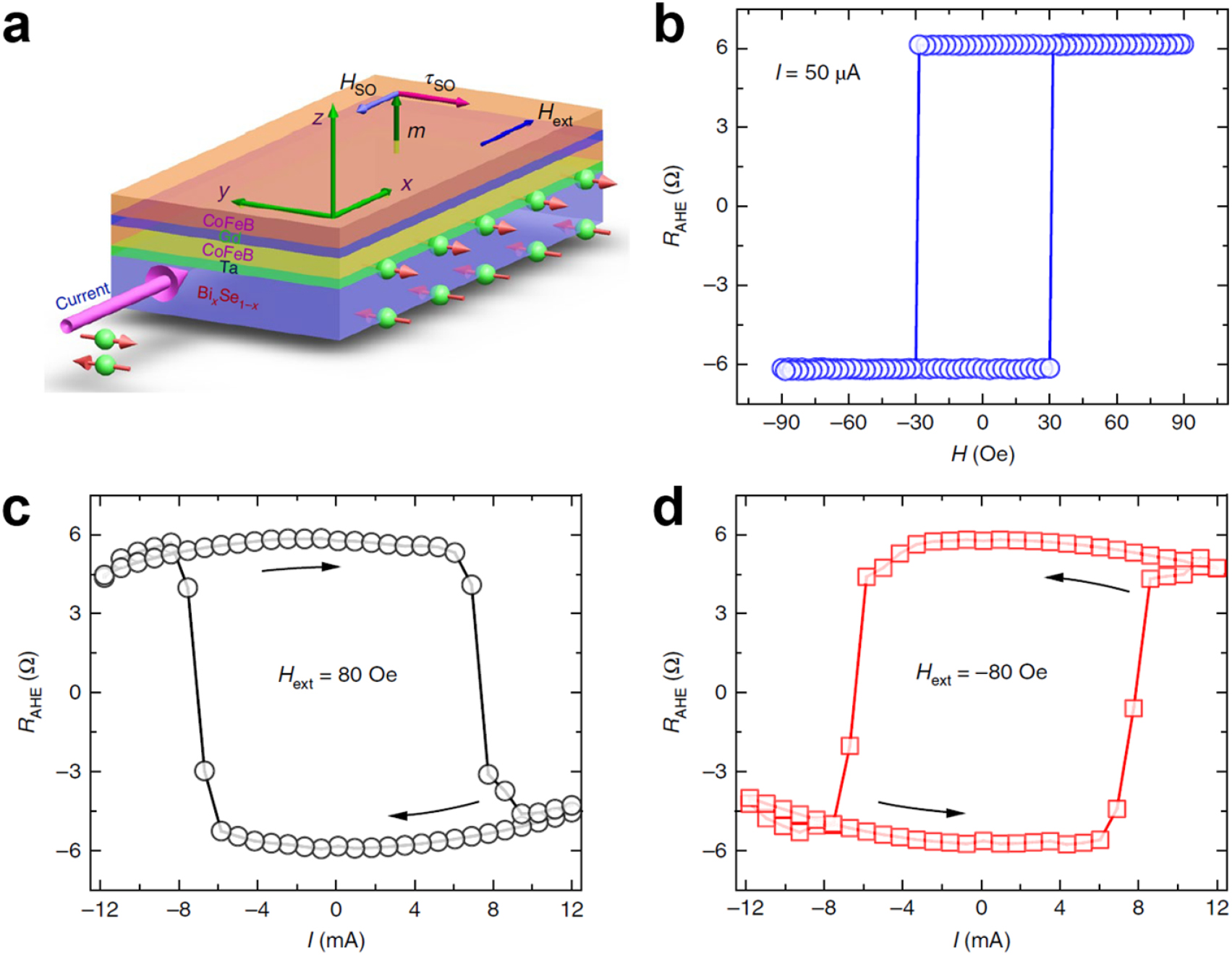
Figure 33. Vector plot of the pair spin polarisation (103) for the Rashba SOC. Vector  shows the average polarisation (104).
Download figure:
Standard image High-resolution image
As we see, in cubic NCSs the pair spin polarisation is locked parallel to the applied current.
The charge-spin conversion is an indicator of the unconventional, mixed-parity order parameter. Still, the direct magnetoelectric effect has not been verified experimentally yet despite a diverse range of other observed properties6. On the other hand, a growing body of theoretical predictions may help in planning a decisive experiment. Some specific predictions include spin Hall effects and nonequilibrium spin accumulation in superconducting structures [556, 639–641], electrically controllable spin filtering in TI surfaces states [595], equal-spin Andreev reflection due to the induced nonunitary pairing [596, 627], magnetoelectric  transitions in quantum spin Hall insulators [558], the generation of a transverse spin supercurrent by a charge supercurrent [642], and the long-range effect of a Zeeman field on the electric current in an Andreev interferometer [643].
12. Outlook
In closing we give a brief overview of future directions. In topological insulators the contrast between quantum anomalous Hall research, which focuses on dissipationless transport at very low temperatures, and spin–orbit torque devices, which are aiming for room-temperature operation, is noteworthy. As a result of the latter several gaps remain in our understanding of spin–orbit torques at very low temperatures, for example the role of quantum interference effects such as weak localisation and anti-localisation. The exact origin of the anti-damping torque continues to be hotly debated, with possibilities including the spin Hall effect, the Berry curvature anomalous Hall term, which may however be overwhelmed by disorder, and spin–orbit scattering mechanisms that have not been fully explained. A related question, to date unsettled, is whether it is possible for an anti-damping torque to exist without the spin-Hall effect. In simple analytical models, the final result to this question is very sensitive to the starting Hamiltonian.
Furthermore, whereas the bulk of attention has focused on ferromagnets, antiferromagnets are also generating excitement [644, 645] and will no doubt witness considerable growth. Traditional problems from magnetism, such as current-driven domain wall motion, have yet to take off in topological materials. Spin-momentum locking offers new functionalities for magneto-resistive devices such as spin valves, since electrons travelling in a specific direction have a fixed spin orientation determined by their momentum. Experimentally, there is a lot of space to investigate van der Waals heterostructures where experiments are just beginning [646].
A fundamental gap in the theoretical approach to spin–orbit torques as well as non-linear response is the method used to handle the spin current. It is well known that in spin–orbit coupled systems the proper definition of the spin current is not  , where
  and
and  represent the spin and velocity operators respectively, as that current is not conserved, but
  , with
  the position operator. This is motivated by spin non-conservation in the presence of spin–orbit coupling (an enlightening strategy for circumventing these ambiguities is described in [647]). Whereas the position operator is a difficult quantity to handle, in particular in bases of Bloch states, in which most such calculations are attempted, a complete understanding of spin–orbit torques in topological materials will remain elusive until the magnitude of the proper spin current is determined.
Important unanswered questions in anomalous Hall transport include the role of spin-charge correlations, which has only recently begun to receive attention [188]. Moreover, according to a number of experiments, the sign of the anomalous Hall conductivity can be the same [648–650] as or differ [180, 648, 651–653] from that of the intrinsic contribution [654–657], depending on the magnetic doping concentration. This puzzling observation has thus far not received an unambiguous explanation. Likewise, the role of disorder in the anomalous Hall contribution due to Fermi arcs in WSMs has not been elucidated. The anomalous Hall effect is being explored in Dirac systems with spin, pseudospin and valley degrees of freedom [658], whose behaviour is qualitatively different from TIs. With the possibility of achieving strong spin–orbit coupling in graphene, one can envisage further research on this topic. In skyrmions studies it is assumed the skyrmion texture remains unaffected by the electrons at the interface, an assumption that remains to be verified by further research. Anomalous Hall transport affects Coulomb drag [659]. Finally, topological effects are also present in linear and non-linear thermal transport [660, 661].
The understanding of interband coherence effects on the non-linear optical response is in its infancy. This applies both to interband transitions induced by Berry curvature terms as well as the role of scattering, whether by disorder, phonons or magnons, and the examination of effects known to be important in transport such as skew scattering, side-jump, localisation and Kondo physics. To add to this, the vast majority of work on optical systems has focused on the case of an undoped conduction band, while potential Fermi surface effects in doped systems have not been explored.
Another exciting avenue for future research is the exploration of chiral superconductivity, non-Abelian excitations and unconventional Cooper pairing in topological materials. These topics remain a subject of intense experimental and theoretical effort. The experimental quest for chiral superconductivity in both intrinsic and proximity-induced superconductors continues. Speaking of hybrid proximity structures, we have seen that the chiral superconductivity can be understood as the duality between a  —superconductor and a Chern insulator. Is there more new physics beyond this intricate duality? The answer to this question is not only of theoretical interest, but may also uncover hitherto unexplored routes towards topological quantum computation and superconducting spintronics.
Finally, we would like to emphasise that the topological zoo continues to grow, with Moire heterostructures expected to exhibit a variety of topological phases, which lately have been shown to include a quantised anomalous Hall effect in the absence of doping [213] due to strong electron-electron interactions leading to flat-band ferromagnetism. The prospects for future developments in 2D topological materials transport remain as rich as ever.
Acknowledgments
DC would like to thank Branislav Nikolić for a series of instructive discussions and to acknowledge the stimulating input of Di Xiao, Shulei Zhang, Giovanni Vignale, Allan MacDonald, and Oleg Tretiakov. YL thanks N Liu, X F Niu and Z C Wang for technical assistance, and X Dai, Z Fang, K He, H Z Lu, A D Mirlin, S Q Shen, J R Shi, H M Weng, P Xiong and X C Xie for valuable discussions. GT thanks Ulrich Eckern, Sebastian Bergeret, Alexander Golubov, Yukio Tanaka and Dieter Weiss for their valuable comments. This work was supported by the Australian Research Council Centre of Excellence in Future Low-Energy Electronics Technologies funded by the Australian Government, by the National Science Foundation of China (Project No. 61425015), National Basic Research Program of China (Project No. 2015CB921102), National Key Research and Development Program (Project No. 2016YFA0300600), and Strategic Priority Research Program of Chinese Academy of Sciences (Project No. XDB28000000) and by the German Research Foundation (DFG) through TRR 80.