

Abstract
While two-dimensional (2D) van der Waals (vdW) layered materials are promising channel materials for wearable electronics and energy-efficient field-effect transistors (FETs), large hysteresis and large subthreshold swing induced by either dangling bonds at gate oxide dielectrics and/or trap molecules in bubbles at vdW interface are a serious drawback, hampering implementation of the 2D-material based FETs in real electronics. Here, we report a monolayer MoS2 FET with near-zero hysteresis reaching 0.15% of the sweeping range of the gate bias, a record-value observed so far in 2D FETs. This was realized by squeezing the MoS2 channel between top h-BN layer and bottom h-BN gate dielectrics and further removing the trap molecules in bubbles at the vdW interfaces via post-annealing. By segregating the bubbles out to the edge of the channel, we also obtain excellent switching characteristics with a minimum subthreshold swing of 63 mV/dec, an average subthreshold slope of 69 mV/dec for a current range of four orders of magnitude at room temperature, and a high on/off current ratio of 108 at a small operating voltage (<1 V). Such a near-zero hysteresis and a near-ideal subthreshold limit originate from the reduced trap density of ~5.2 × 109 cm−2 eV−1, a thousand times smaller than previously reported values.
Export citation and abstract BibTeX RIS
1. Introduction
Since Si technology is fast approaching fundamental limit to shrink the gate length due to poor gate electrostatic control in the channel [1, 2], Moore's law that the number of transistors in an integrated circuit chip doubles approximately every two years is no longer valid [2, 3]. 2D vdW layered materials is one of a candidate to replace Si because of their excellent electronic properties [4–10]. Monolayer MoS2 is atomically thin (~0.7 nm) and exhibits lower in-plane dielectric constant (~4) compared to bulk Si (~11.7), which enhances the gate controllability over the channel and does not limit the scaling of the gate length down to the ~1 nm [8]. This opens a new possibility for scaling of transistors dimension for high integration circuit.
In 2D vdW materials, because of large surface/volume ratio, the interface between the 2D channel material and the gate dielectric plays a crucial role. High-k dielectric oxide materials such as Al2O3 [11], HfO2 [4, 12], ZrO2 [8, 13] and Y2O3 [14] employed in the fabrication of gate insulators have numerous dangling bonds and large surface roughness. The dangling bonds act as traps, thereby inducing scattering of charge carriers and leading to low carrier mobility in the 2D FETs [15–17]. Hexagonal boron nitride (h-BN), inert and dangling bonds free 2D-dielectric layer, has been previously employed as an encapsulation layer to improve the mobility [18–20]. However, the bubbles of trapped adsorbates formed during stacking of 2D materials on h-BN substrate seriously affect the quality of heterointerfaces and induce unexpected phenomena [21–26]. Using h-BN as an encapsulation layer, the mobility was significantly enhanced up to 34 000 cm2 V−1 s−1 at low temperature [18]. However, other important parameters, such as hysteresis and subthreshold swing were not reported. In another report, even the hBN encapsulated MoS2 was highly stable, the device still showed a hysteresis of 3% for few-layer MoS2 [19]. Hence, trapped adsorbates in bubbles at the vdW interfaces are an inherent and challenging problem which can cause the uncertainties in device operation.
In this study, we demonstrated bubble-free h-BN/MoS2/h-BN vdW interface, thereby achieved near-zero hysteresis as well as near-ideal subthreshold swing. By removal of trapped adsorbates in the bubble at the vdW interfaces of graphene/h-BN/MoS2/h-BN heterostructure through the post-annealing [27–31], we achieved ultra-low hysteresis of 0.15%, 20 times smaller than best-reported values [19]. Using the low noise frequency measurement, the surface trap density in our FET was estimated to be 5.2 × 109 cm−2 eV−1, three orders of magnitude lower than that of previous reports in the literature. Therefore, a near-ideal subthreshold swing of 63 mV/dec was achieved in the MoS2 FET at room temperature. In addition, by optimizing the h-BN thickness, the device can work at a small operating voltage of 1 V with a high on/off ratio of 108. Our study demonstrates the potential of h-BN as a dielectric material for the fabrication of low-voltage and low power transistors in the future.
2. Result and discussion
2.1. Device structure and performance
The monolayer MoS2-based FET consists of a graphene layer as a back-gate electrode, the bottom thick h-BN (h-BNb) as a gate insulator, a monolayer MoS2 as a channel and the top thick h-BN (h-BNt) as a passivation layer (see figure 1(a) for the illustration of the FET). The optical image of the device is displayed in figure 1(b) and the fabrication process can be found in the experiment section and figure S1 (supporting information (stacks.iop.org/TDM/5/031001/mmedia)). The peaks corresponding to graphene, h-BN, and MoS2 were observed in the Raman spectrum of the graphene/h-BNb/MoS2/h-BNt stack (see figure S2). The monolayer nature of MoS2 was confirmed from the wavenumber difference of 18 cm−1 between A1g (~403 cm−1) and  (~385 cm−1) peaks (see inset in figure S2) [32]. Atomic force microscopy (AFM) measurements were conducted after the sample annealed at 300 °C for 5 h in an H2/Ar atmosphere (H2/Ar ratio of 50/200 sccm) to ensure a clean MoS2 channel. We observed the formation of a few air bubbles near the edge of MoS2 flake. However, the interface of MoS2 channel remained clear of any bubbles (see inset in figure 1(c)). Figure 1(c) shows the I–V characteristics of our monolayer MoS2 FET for an h-BN gate dielectric thickness of ~8 nm (leakage current is shown in figure S3). Along with an on/off ratio of 109, the monolayer MoS2 FET was nearly free from hysteresis with only 0.15% (ΔV/Vg) over the entire range of current (ranging from 10−14 to 10−5 A) (figure 1(d)), which is the smallest value reported in 2D FETs so far. In addition, despite h-BN low dielectric constant of ~4, the FET exhibited a remarkably steep subthreshold swing of 63 mV/dec, very close to the thermal limit (60 mV/dec) and an average subthreshold swing (SS) of 69 mV/dec over four orders of current (figure 1(d)). The device was also measured under ambient condition, low vacuum (10−2 Torr) and high vacuum (10−6 Torr), there is no significant difference in I–V characteristic between measurements (figure S4).
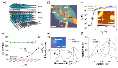
Figure 1. Device structure and performance. (a) Schematic of the device. (b) Optical image of the device, the thickness of h-BNb and h-BNt were 8 and 4 nm, respectively. (c) Typical I–V characteristic of a MoS2 FET for the different source-drain voltages. The inset shows atomic force microscope image recorded around the MoS2 channel. (d) Subthreshold swing and hysteresis as the function of current (extracted from (c)). The red-dashed line indicates the thermal limit of subthreshold swing and the light-blue line indicates the average subthreshold swing over 4 orders of current. Raman (e) and PL spectrum (f) taken at the bubbled and flat area as shown in the inset in (c). The orange arrows show the red shift in Raman peaks and PL peaks (inset in f). The scale bars are 5 µm in (b) and 2 µm in (c).
Download figure:
Standard image High-resolution imageThe high performance of our FET is attributed to the ultra-clean interfaces of graphene/h-BN/MoS2/h-BN heterostructure at the channel area which is not influenced by trapped adsorbates. To see the effect of bubbles on the properties of MoS2, we conducted Raman and photoluminescence (PL) measurement at the flat area and bubbled area before annealing (inset in figure 1(e)). We found the redshifts at  peak in Raman spectrum in the bubbled area (figure 1(e)), although the peak shift in A1g is negligible. The PL intensity is also reduced (figure 1(f)) and the A exciton peak shows the redshift (inset in figure 1(f)), possibly from the domination of negative trions. These indicate that the n-doping is applied in the bubbled area [33, 34]. Doped molecules trapped in the bubble (H2O, O2...) are origins of the trap states which increase hysteresis or subthreshold swing. The removal of bubbles is, therefore, necessary to preserve intrinsic properties of MoS2 to enhance the performance of the device.
2.2. Effect of annealing on the interface of the vdW heterostructure
To study the surface roughness of heterostructure which is an important factor in the charge transport in the channel, atomic force microscope (AFM) measurements were conducted. Before annealing samples, we observed rich air trap bubbles formed during the transfer process with the sizes less than 1.5 mm in diameter at the heterointerfaces (white dots in figure 2(a)). These bubbles are distributed homogeneously over the entire channel with the thickness variation from 0 to 20 nm. These bubbles induce a large root mean square surface roughness (Rrms) of 4.2 nm (figure 2(b)) and a large profile roughness (Ra) of 3.0 nm (figure 2(c)). While the rough surface will cause the charge scattering and therefore reduce the mobility, adsorbates in the bubbles result in large hysteresis and subthreshold swing. In order to remove the trapped adsorbates to improve quality of the heterointerfaces, samples were then annealed with the same condition as mentioned above. During the thermal annealing process, the bubble residues are decomposed and desorbed from the surfaces, at the same time, because of high kinetic energy under high temperature, the tiny bubbles at the heterointerfaces are able to migrate and merge with adjacent bubbles to form bigger bubbles via Ostwald ripening process, which are eventually out-diffused into the edge of the channel, leaving a large and flat area in the channel (inset in figures 1(c) and 2(d)). As shown in figures 2(d)–(f), the surface roughness is significantly reduced after annealing, the Rrms and Ra are reduced to 0.6 and 0.4 respectively, 7 times less than those of samples before annealing. We also note that the samples can be damaged in some cases because of extremely vigorous movement of the bubbles.

Figure 2. Effect of annealing on the interface of the vdW heterostructure. AFM images (a) and (d), surface roughness (b) and (e) as well as the height profile (c) and (f) of graphene/h-BNb)/MoS2/h-BNt stacking (before, after annealing) respectively. White dot spots represent the air trap bubbles. The scale bars are 2 µm in (a) and (d) and 0.5 µm in (b) and (e).
Download figure:
Standard image High-resolution image2.3. Effect of passivation and annealing on the device performance
To investigate the effect of annealing on the device performance, we measured I–V characteristics of the FETs with no passivation, passivation with the top h-BN, as well as passivation and annealing (figures 3(a)–(c)). A large hysteresis is observed when there is no passivation (figure 3(a)). The hysteresis is then significantly reduced after h-BN passivation but not completely removed due to the remaining air or adsorbates within the bubbles (figure 3(b)). After annealing, the bubbles are removed and consequently, almost no hysteresis is observed, as shown in figure 3(c). Figure 3(d) illustrates the hysteresis in the device as a function of current extracted from the I–V curves. The hysteresis is predominantly suppressed over the entire range of current after annealing due to the formation of a clean interface as discussed earlier. We tested 5 more devices to confirm the consistency. All the samples showed reduction of bubble portion in MoS2 channel after annealing and improvement of electrical characteristics, four samples showed the subthreshold swing less than 71 mV/dec and hysteresis of <0.2% (figure S5) and one sample showed the subthreshold swing of 105 mV/dec and hysteresis of 2% (figure S6) with partially remained bubbles on the channel area. The shifting of the threshold voltage toward the positive gate bias (figures 3(a)–(c)) reveals the reduction of n-doping in the MoS2 channel, consistent with the PL and Raman data in figures 1(e) and (f). The subthreshold swing is also improved significantly after passivation and being close to the thermal limit (60 mV/dec) after annealing (figure 3(e)). This originates from the reduction in the air bubbles density at the interface as displayed in figures 2(d)–(f). The improvements in the interface also result in the increase by 4 times in the charge carrier mobility, from 10 to 40 cm2 V−1 s−1 at Vg−Vth of 6 V (figure 3(f)). The enhancement of mobility is attributed to reducing the trap state at the interfaces as well as improving the contact resistance after encapsulation and annealing. The output characteristic and mobility calculation are provided in supporting information (figures S7, S8 and Note 1).

Figure 3. Effect of passivation and annealing on the device performance. (a)–(c) I–V curves of the device before passivation (a), after passivation (b) and after annealing (c). The schematic displayed in the insets depict the interfacial states at each stage with the representative molecules (H2O or O2) between the MoS2/h-BN and the h-BN/Graphene interfaces. Hysteresis, subthreshold swing and mobility are displayed in (d)–(f) respectively.
Download figure:
Standard image High-resolution image2.4. The interfacial trap density measurement
The interfacial trap states are the origin of the hysteresis in 2D FETs, thus, removing these trap states is key to suppress the hysteresis. The interfacial trap density (Nit) and interfacial trap density distribution per energy (Dit) can be calculated from the hysteresis and subthreshold swing, respectively (see Note 2, supporting information for details). Due to the clean interface, there was a significant reduction in the Nit (Dit) for nearly 40 times after encapsulation and annealing (figure 4(a)).
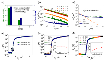
Figure 4. Device performance and noise analysis. (a) Normalized interface trap density (represented by Nit or Dit) before passivation, after passivation and after annealing. (b) Noise spectra SI as a function of different gate bias at Vds = 0.5 V. (c) Fitting of the noise features of the device (dark-green dots) at f = 10 Hz with the CNF + CMF model (navy line) and the CNF model (orange-dashed line). I–V curves of the device for different sweeping direction (d), sweeping rates (e) and sweeping ranges (f). Insets in (e) and (f) show absolute hysteresis at the threshold voltage.
Download figure:
Standard image High-resolution imageTo further investigate quantitatively the interfacial traps, we conducted a low-frequency noise measurement [35], with the frequency ranging from 1 Hz to 1000 Hz (figure 4(b)). The noise spectral density SI shows a general 1/f trend from the subthreshold regime to high accumulation regime, thereby revealing that the trap states are uniformly distributed in the momentum and real space. The noise source may arise from carrier-number fluctuation (CNF) or mobility fluctuation in the channel. The data from low-frequency noise analysis were well described by the carrier-number fluctuation and correlated mobility fluctuation (CNF + CMF) model instead of the CNF model only. By fitting the measured noise data at 10 Hz with (CNF + CMF) model [35, 36], we confirm that the trap states are induced at the h-BN/MoS2 interface (figure 4(c) and Note 3, supporting information). We have also extracted the charge trap density using the CNF + CMF model. Our device exhibits a charge trap density of 5.2 × 109 cm−2 eV−1, thousand times less than that of previous reports using 2D transition metal dichalcogenides (TMD) on other substrates [37–40]. We attribute the low charge trap density to arise from the clean vdW interfaces without the presence of the trapped molecules and the lacking of dangling bonds between h-BN and MoS2 layers.
With the presence of large trap states at the interfaces, the hysteresis strongly depends on the external factors such as sweeping direction, sweeping rate, and sweeping range [17]. We measured the I–V with different sweeping directions (figure 4(d)), sweeping rates (figure 4(e)), and sweeping ranges (figure 4(f)) of the gate bias. All threshold voltages are almost identical (figures 4(d)–(f)) and the hysteresis is less influenced by sweeping rate and sweeping range of the gate bias (insets in figures 4(e) and (f)). These imply that the I–V characteristic is nearly independent of those external factors in our samples by the low trap density at the interfaces.
2.5. h-BN thickness dependence
Although a thin h-BN film appears to be desirable for gate controllability and achieving a low subthreshold swing, gate leakage current can arise from the direct tunneling of charge carriers through the thin h-BN barrier. To examine the dependence of electrical characteristics of the FET on the h-BN thickness, we fabricated MoS2 FETs with various h-BN thicknesses ranging between 2 to 20 nm and measured the break-down voltage Vbd at leakage current of 1 nA (Note 4, figure S9, supporting information). The breakdown electric field increases from 0.0001 V nm−1 to ~0.6 V nm−1 and saturates at an h-BN thickness of ~8 nm (figure 5(a)). This transition occurs because of a transition from direct to Fowler–Nordheim tunneling [41]. Figure 5(b) shows the dependence of the h-BN thickness on the on-current, off-current and on/off current ratio at a source-drain voltage of 0.5 V and a gate bias sweeping from −5 to 5 V. The on/off ratio increases from 102 to 109 when the h-BN thickness is ~8 nm, mostly due to a drop off in the off-current. The off-current is generated by the tunneling leakage current, which is reduced to less than 10−14 A (limited by the range of our source measurement unit) for an h-BN thickness >8 nm, while the on-current slightly decreases due to the reduction in the gate electric field. Based on these measurements, we conclude that the h-BN thickness is optimal at ~8 nm. A low threshold voltage is essential for the low power consumption of the device. The threshold voltage Vth can be scaled down with a small operating voltage of less than 1 V while still maintaining a high on/off ratio of 108 at the h-BN thickness of ~8 nm (figures S10 and 5(c)). Since the dielectric constant of h-BN is quite small (ε ≈ 4) compared to other high-k materials such as Al2O3 (ε ≈ 9), HfO2 (ε ≈ 18) or ZrO2 (ε ≈ 25), the small subthreshold swing as well as negligible hysteresis presented in our device is attributed to the clean interfaces without dangling bonds of 2D materials rather than the dielectric constant value. We compare our device performance (in terms of subthreshold swing and on/off ratio) with previous literature reports on MoS2 devices [4, 8, 9, 19, 42–46]. Our device exhibits the highest on/off ratio, as well as the smallest subthreshold swing among the conventional MoS2 FETs fabricated using different dielectric gates (figure 5(d)).

Figure 5. h-BN thickness dependence. (a) Break-down electric field (Ebd) as a function of h-BN thickness (th-BN). (b) Off-current, on-current and on/off ratio of the MoS2 FET for different thickness of h-BN. Dots are measured data and solid lines are guide lines for eyes. (c) Threshold voltage of the MoS2 FET for the different h-BN thicknesses. (d) Comparison of the on/off current ratio and the subthreshold swing of our device in comparison to previously published MoS2 FETs. The numbers in bracket denote the references.
Download figure:
Standard image High-resolution image
3. Conclusion
In conclusion, we have demonstrated a new approach for the realization of the near-zero hysteresis and the ultimate thermal limit of the subthreshold swing by adopting the thin h-BN layers for both the gate dielectric and passivation layer in a monolayer MoS2 transistor. The surface trap density is minimized to 5.2 × 109 cm−2 eV−1, thus resulting in an ultralow hysteresis of 0.15% with a steep subthreshold swing of 63 mV/dec. Furthermore, the threshold voltage scales down the operating voltage to less than 1 V by optimizing the thickness of h-BN (to ~8 nm), while maintaining a high on/off current ratio of ~108. Our results highlight the potential of h-BN as an exceptional dielectric material and passivation layer for the fabrication of low-voltage green and tunnel FETs in the future.
4. Materials and methods
4.1. Preparation of graphene/h-BN/MoS2/h-BN stacks
The graphene/h-BN/MoS2/h-BN stack was fabricated with a bottom-up assembly method involving multiple wet and dry transfers [23, 47, 48]. In the first step, graphene flakes (which act as the back-gate electrode) were synthesized using chemical vapor deposition (CVD). The graphene was transferred onto a Si substrate with a 300 nm-thick SiO2 coating by the wet bubble transfer method. In the next step, we prepared poly (methyl methacrylate) (PMMA)/poly (vinyl alcohol) (PVA)/300 nm SiO2/Si substrates and separately exfoliated h-BN, MoS2 flakes onto the substrate via mechanical exfoliation with a Scotch tape. The exfoliated h-BN flakes (serving as the gate dielectric layer (h-BNb)) with thicknesses in the range of 3–20 nm were selected for deposition on top of graphene. The thicknesses of the h-BNb were confirmed by AFM after electrical measurements. After the dissolution of PVA in hot water, the h-BN/PMMA film was detached from the substrate and floated on the water surface. We used a special holder with a hole to pull out h-BN/PMMA film and load it onto micro-manipulator in a reverse manner. Then, the desired h-BN flake was aligned with the target graphene on 300 nm SiO2/Si substrate and held in contact for 15 min at 140 °C to ensure that PMMA film was entirely isolated from the holder. A similar process was employed to transfer the MoS2 monolayer flake on top of the h-BNb. The source (S), drain (D), and gate (G) were fabricated using a combination of e-beam lithography followed by the deposition of Cr/Au (10/50 nm). Finally, another h-BN flake (h-BNt) was transferred on top of the graphene/h-BN/MoS2 stack, thereby forming a passivated MoS2 channel structure. In the last step, all samples were annealed at 300 °C for 3 h in a H2/Ar atmosphere (H2/Ar ratio of 50/200 sccm). The complete sequence of the whole fabrication is illustrated in figure S1 with the help of optical microscope images.
4.2. Device characterization
The AFM images of the samples were recorded using an SPA400 (SEIKO) atomic force microscope. Raman spectrums were measured using the Witec system (532 nm wavelength). All electrical transport measurements were performed in high vacuum (10−6 Torr) unless it is mentioned with a probe station and source/measure units (Keithley 4200 and Agilent B2900A).
Acknowledgments
This work is supported by the Institute for Basic Science (Grant No. IBS-R011-D1). WJY acknowledges the HRD program (Grant No. 20144030200580) of the KETEP grant funded by the KGMT and the Basic Science Research Program through the NRF funded by the Ministry of Science, ICT & Future Planning (NRF-2015R1C1A1A02037387).
Author contributions
YHL, WJY, QAV conceived the research and designed the experiment. QAV and SF performed most of the experiments including device fabrication, characterization and data analysis. SHL prepared the CVD graphene samples. M-KJ performed low frequency noise measurement and analysis. YHL, QAV wrote the paper. All authors discussed the results and commented on the manuscript.
Additional information
Supplementary information accompanies this paper at http://iopscience.iop.org/
Competing financial interests
The authors declare no competing financial interests.