
Abstract
The ballistic motion of electrons in graphene opens exciting opportunities for electron-optic devices based on collimated electron beams. We form a collimating contact in a hBN-encapsulated graphene hall bar by adding zigzag contacts on either side of an electron emitter that absorb stray electrons; collimation can be turned off by floating the zig-zag contacts. The electron beam is imaged using a liquid-He cooled scanning gate microscope (SGM). The tip deflects electrons as they pass from the collimating contact to a receiving contact on the opposite side of the channel, and an image of electron flow can be made by displaying the change in transmission as the tip is raster scanned across the sample. The angular half width Δθ of the electron beam is found by applying a perpendicular magnetic field B that bends electron paths into cyclotron orbits. The images reveal that the electron flow from the collimating contact drops quickly at B = 0.05 T when the electron orbits miss the receiving contact. The flow for the non-collimating case persists longer, up to B = 0.19 T, due to the broader range of entry angles. Ray-tracing simulations agree well with the experimental images. By fitting the fields B at which the magnitude of electron flow drops in the experimental SGM images, we find Δθ = 9° for electron flow from the collimating contact, compared with Δθ = 54° for the non-collimating case.
Export citation and abstract BibTeX RIS
1. Introduction
Ballistic graphene devices open pathways for new electronic and photonic applications [1–6]. Electrons move through graphene at a constant speed ~106 m s−1 as if they were photons, and they easily pass through potential barriers via Klein tunneling, as electrons change into holes, due to the gapless bandstructure [7–12]. The differences between the two-dimensional electron gas (2DEG) in graphene and GaAs/AlGaAs heterostructures present challenges to understanding the device physics, and offer new types of devices that make use of graphene's virtues. The ballistic motion of electrons through a device can be controlled by using magnetic focusing—in a perpendicular magnetic field B electrons emitted from a point contact refocus at a second point contact located a cyclotron diameter away [13, 14]. Magnetic focusing has been demonstrated in ballistic GaAs 2DEGs [15, 16] and in graphene [17, 18]. The angular distribution of the lowest quantum mode of a quantum point contact (QPC) provides a degree of collimation in a GaAs 2DEG [19–21], but a more tightly directed electron beam is desirable. A collimated beam has been formed in GaAs in flow between two separated QPCs [22], and by using an electrostatic lens [23]. Graphene has the ability to create a negative index of refraction [24, 25] for electron waves, allowing a lateral p-n junction to act as a lens that focuses electron waves [11, 26, 27]. For ballistic electronics, a narrow, collimated electron beam with the electrons pointed in the same direction would be ideal. Recently a collimating contact for electrons in graphene has been demonstrated via transport measurements [28].
In this paper, we demonstrate that a collimating contact can produce a narrow electron beam in graphene by imaging the pattern of electron flow using a cooled scanning gate microscope (SGM). We have adapted a technique previously used to image electron flow through a GaAs 2DEG [16, 19–21] and graphene [18, 29], and we now use this technique to image the pattern of electron flow from a collimating contact in graphene. The collimating contact is formed by a rectangular end contact with zigzag side contacts on either side that form a collimated beam of electrons inside the sample. Images of electron flow confirm that the collimating contact substantially narrows the electron beam. A quantitative measure of angular width of the electron beam is obtained by applying a perpendicular magnetic field B to bend the electron trajectories into cyclotron orbits, so they miss the collecting contact, reducing the intensity of electron beam image. A fit to ray tracing simulations gives a (HWHM) angular width Δθ = 9° for the collimating contact and much wider width Δθ = 54° when collimation is turned off.
2. Methods
2.1. Collimating contact device
The geometry of the collimating contact is shown in figure 1(a), an SEM image of the Hall-bar graphene sample; the white square indicates the imaged region. The Hall bar (blue region) is patterned from a hBN/graphene/hBN sandwich. It has dimensions 1.6 × 5.0 µm2, with two collimating contacts (yellow) along each side, separated by 1.6 µm, and large source and drain contacts (width 1.6 µm) at either end. The four collimating contacts have an end contact that emits electrons and two zigzag side contacts that collimate the electron beam by absorbing electrons. The device sits on a heavily doped Si substrate which acts as a back-gate, covered by a 285 nm thick insulating layer of silicon oxide (SiO2). The top and bottom hBN flakes along with the graphene are mechanically cleaved. Using a dry transfer technique, the flakes are stacked onto the SiO2 substrate. To achieve highly transparent metallic contacts to the graphene, we expose the freshly etched graphene edge with reactive ion etching and evaporate chromium and gold layers immediately afterwards [30].

Figure 1. (a) Scanning electron micrograph of hBN-graphene-hBN device in a hall bar geometry with four collimating contacts with absorptive zig-zag sections that form a narrow electron beam. The white square shows the area imaged by the cooled SGM. The blue region indicates graphene and yellow indicates metal contacts. (b) Ray-tracing simulations of electrons passing through the collimating contact (yellow) through absorptive zig-zag side contacts (yellow) the half angle of exiting rays in the schematic diagram is Δθ = 7.5°. (c) Simulated image charge created by the charged tip which creates a local dip in electron density.
Download figure:
Standard image High-resolution imageFigure 1(b) shows ray-tracing simulation of electron trajectories passing through a collimating contact, which consists of an end contact (yellow) that emits electrons into the graphene and zigzag side contacts on either side (yellow) that form a series of constrictions. Electrons emitted from top narrow contact enter at all angles. Collimation is turned on by grounding the zigzag side contacts—stray electrons entering at wide angles hit the zigzags and are absorbed—only electrons that pass through the gap get through, producing a narrow electron beam. The collimating contact can be turned off by simply connecting the top contact to the two zigzag side contacts. In this case, the combined contact behaves as a single source of electrons with a wider width and no collimation.
2.2. Cooled SGM
We have developed a technique that uses a cooled SGM to image the flow of electrons through a 2DEG that we used for GaAs/AlGaAs heterostructures [16, 19–21] and graphene samples [18, 29, 31]. The charged tip creates an image charge in the 2DEG below (figure 1(c)) that deflects electrons away from their original paths, changing the transmission T between two contacts of a ballistic device. An image of the electron flow is obtained by displaying the change in transmission ΔT as the tip is raster scanned across the device.
In this paper, we used this approach to image electron flow from a collimating emitter contact at the top of the graphene sample in the area indicated by a white square in figure 1(a) to a non-collimating collector contact at the bottom of the sample. With the tip absent, electrons pass ballistically through the channel between the emitter and the collector contacts. The shape of the electron beam is imaged by displaying the change in transmission ΔT versus tip location as the SGM tip scatters electrons away from their original paths, as the tip is raster scanned across the sample. We measure voltage difference ΔV between contacts 3, 5, and 6 tied together, and contact 4. One can determine ΔT from the change in voltage ΔV at the ungrounded collecting contact for a current I into the emitting contact. As electrons accumulate, raising the electron density, the chemical potential increases, creating an opposing current that maintains zero net current flow. By measuring the voltage change ΔV or the transresistance change ΔR = ΔV/I at the receiving contact, the transmission change ΔT induced by the tip can be obtained [18, 31]. For a collimated electron beam, the current is emitted from contact 1 to contact 2 in figure 1(a), while contacts 7 and 8 are grounded to collect sideways moving electrons. To turn collimation off, contacts 1, 7 and 8 are connected together as a single current emitter while contact 2 is grounded. The collecting contact always has collimation turned off with contacts 3, 5 and 6 connected together.
The width of the emitted electron beam is substantially reduced when collimation is turned on for the top contact. To obtain a quantitative measure of the angular width of the emitted electron beam, we apply a perpendicular magnetic field B that bends electron paths into cyclotron orbits. The curvature causes electrons to miss the collecting contact and reduces the intensity of the imaged flow.
2.3. Electron path simulations
Bending electron trajectories with a perpendicular magnetic field B is used to measure the angular width θ of the emitted electron beam in the experiments below. We use a ray-tracing model of electron motion and tip perturbation to simulate the electron flow through graphene in this case [18, 31]. Our model computes the transmission of electrons between two contacts in graphene for each tip position. The electrons trajectories from the emitter contact are traced by considering two forces: (1) the force from the tip induced charge density profile, and (2) the Lorentz force from B.
The work function difference between the Si SGM tip and graphene creates a change in electron density Δntip in the graphene below the tip. For a tip with charge q at a height h above the graphene sheet, the change in density Δntip at a radius a away from the tip position is
where e is the electron charge. The tip is modeled as a conducting sphere with the tip radius r = 10 nm, and the conical shaft as a much larger sphere that fits in the wide end of the cone, held at the same potential [18, 21]. This two-sphere model is in good agreement with numerical solutions for the electrostatics of the actual conical tip [21]. The tip height h = 70 nm is dominated by the hBN encapsulating layer with dielectric constant ε ~ 3 [32]. In the simulations, we choose a peak density change Δntip(0) = −5 × 1011 cm−2 at a = 0 to match the experimental data. This change is smaller than the electron densities, which are n = 1.08 × 1012 cm−2 for the images in figure 2, and range from n = 0.72 × 1012 cm−2 to n = 1.80 × 1012 cm−2 for the images in figures 3 and 4. The local drop in electron density Δntip(a) caused by the tip reduces the Fermi energy EF = ħvF(πn)1/2 locally to EF(a) = EF(n + Δntip). For the electron density n = 1.08 × 1012 cm−2 the Fermi energy is EF = 0.125 eV with no tip present, and it is locally reduced by 0.04 eV to EF(0) = 0.085 eV immediately below the tip. The total electrochemical potential, given by EF(a) + U(a) where U(a) is the electrostatic potential due to capacitive coupling to the tip, must be constant in space. Taking a spatial derivative yields the force  on electrons in graphene passing nearby the tip position. The resulting acceleration of an electron due to the tip at position
  using the electron dynamical mass m* = ħ(πn)1/2/vF [18, 31] is:

Figure 2. (a) SGM image of electron flow from the non-collimating top contact to the non-collimating bottom contact (figure 1(a)). (b) SGM image of the electron flow when the collimation is turned on in the top contact (see text) (figure 1(b)). (c) Simulated image of electron flow from the non-collimating top contact to the non-collimating bottom contact. (d) Simulated image of electron flow when collimation is turned on in the top contact. All images at zero magnetic field B = 0 T and electron density n = 1.08 × cm−2. The orange bars on the top and bottom of each image show the contact locations.
Download figure:
Standard image High-resolution image
Figure 3. A magnetic field B was used to measure the angular width of the electron beam emitted into the graphene—the field bends their trajectories and causes them to miss the collecting contact. Tiled experimental SGM images versus B and electron density of (a) electron flow from the non-collimating top contact to the non-collimating bottom contact and (b) electron flow from the collimation top contact. The fields are B = 0 T, 0.025 T, 0.050 T. 0.075 T, 0.100 T, 0.125 T, 0.150 T, and 0.175 T.
Download figure:
Standard image High-resolution image
Figure 4. Simulated images, tiled versus B and n of (a) electron flow from the non-collimating top contact to the non-collimating bottom contact and (b) electron flow when collimation is turned on in the top contact. The fields are B = 0 T, 0.025 T, 0.050 T. 0.075 T, 0.100 T, 0.125 T, 0.150 T, and 0.175 T.
Download figure:
Standard image High-resolution imageThe tip-induced charge density profile creates a force that pushes an electron away from region with low electron density beneath the tip. The Lorentz force F that acts on an electron with velocity v under a magnetic field B is:

In our simulations, we pass N = 10 000 electrons at the Fermi energy into the graphene from the emitting contact. The number of electrons passed from the contact follow a cosine distribution where maximum number of electrons pass perpendicular to the contact. The distribution is cosine within the angular width ±Δθ on either side of the contact while outside of the angular width Δθ no electrons are emitted. The value of Δθ is determined by fitting the image data in figure 5, below. The electron paths are computed by numerically integrating the equation of motion from equations (2) and (3). The transmission T between the top and bottom contacts is then computed by counting the fraction of electrons that reach the non-collimating collecting contact, which has contacts 3, 5 and 6 tied together. An image of electron flow is obtained from the simulations, by displaying the transmission changed ΔT = Ttip − Tnotip versus tip position. The angular width Δθ of the experimental electron beam is determined by using the simulations to fit the image intensity data versus B.
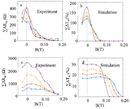
Figure 5. The total magnitude of the electron flow ∑ΔRm, the sum of ΔR in red region between the top and bottom contacts in the SGM images (figure 3) versus B for (a) collimated top contact and (c) non-collimating top contact, together with the total magnitude ∑ΔTm, the sum of ΔT in red region of electron flow in the simulations (figure 4) versus B for (b) collimated top contact and (d) non-collimating top contact, shown at the four electron densities: (purple) n = 0.72 × 1012 cm−2, (yellow) n = 1.08 × 1012 cm−2, (red) n = 1.44 × 1012 cm−2, (blue) n = 1.80 × 1012 cm−2.
Download figure:
Standard image High-resolution imageThe dip in electron density Δntip produced by the SGM tip scatters electrons away from their original trajectories. For an electron originally headed toward the receiving contact, scattering by the tip reduces the transmission, so that a display of ΔT versus tip position shows the original electron paths (red regions in figures 2–4). The half-width of the density dip Δntip from equation (1) is the height h of the tip above the graphene sheet, determined by the thickness of the top hBN layer. The depth of the dip is determined by the difference in work functions between the tip and sample materials. The fixed dip in density produces proportionally greater scattering at low densities and lower scattering at high densities. The density dip below the SGM tip can also increase the transmission T by bumping electrons into the receiving contact from orbits that did not originally go there (blue regions in figures 2–4).
3. Results and discussion
3.1. Images of collimated electron flow
The SGM images of electron flow (figures 2(a) and (b)) and simulated images (figures 2(c) and (d)) clearly demonstrate that the collimating contact significantly narrows the width of the emitted electron beam. Collimation in the top contact is turned off in figures 2(a) and (c) and turned on in figures 2(b) and (d). The experimental images agree quite well with the simulations. In each image, the red regions (ΔT < 0) image the electron flow between the top and bottom contacts by showing where the tip reduces the transmission T by scattering electrons away from their original paths into the receiving contact. As the tip is moved to the side of the electron flow, the blue regions (ΔT > 0) show where the tip increases transmission by knocking electrons that enter at large angles θ into the receiving contact. With the collimation turned off (figures 2(a) and (c)), the electron path (red region) is relatively wide, and the blue regions present on both sides show that many electrons enter at angles too large to be collected by the receiving contact, which are knocked in by the tip. With collimation turned on (figures 2(b) and (d)), the electron path (red region) becomes narrower, and the blue regions go away, confirming that the emitted electron beam has been collimated with fewer electrons entering at wider angles. All these images were obtained at electron density n = 1.08 × 1012 cm−2 and B = 0 T.
3.2. Angular distribution of the electron beam
To measure the angular distribution Δθ of the electron beam emitted into the graphene from the collimating contact, we bent electron paths away from their original directions with a perpendicular magnetic field B, so that some miss the receiving contact. Figures 3(a) and (b) show SGM images of electron flow for the non-collimating and collimating cases respectively, tiled against the magnetic field B and the electron density n. The direct electron flow (red region), is strong at B = 0 and decreases as the magnetic field is increased. With collimation turned off (figure 3(a)), the electron flow persists to much higher fields B = 0.15 T than for or the collimated case B = 0.05 T (figure 3(b)), because the electron paths enter the graphene over a wider range of angles θ. In addition, large blue regions are seen for the non-collimating case (figure 3(a)) on either side of the electron flow (red region) between contacts, because the tip knocks electrons entering at relatively large angles θ toward the receiving contact. The images are stronger at low densities in figure 3(a), where the tip creates a proportionally larger dip in electron density. When collimation is turned on (figure 3(b)), at B = 0 T, blue regions go away, because fewer electrons enter the graphene at large angles. The images in figure 3 show that the angular width Δθ of the electron beam emitted by the collimating contact is much sharper than for the non-collimating case. A quantitative analysis of the experimental images to detertine Δθ is given below.
Figure 4 shows simulated images, tiled against the magnetic field B and the electron density n, that correspond to the experimental images in figure 3, showing the non-collimating (figure 4(a)) and the collimating (figure 4(b)) cases. The simulated and experimental images agree very well, confirming that the collimating contact reduces the angular width Δθ of the emitted electron beam. For these simulations, we input the angular width Δθ = 9° for the collimating case, and Δθ = 54° for the uncollimating case that were determined by fits of simulations to the experimental data, described below. The simulations have the same characteristics as the SGM images: the electron flow (red regions) between the top and bottom contacts is wider for non-collimated case (figure 4(a)) that for collimated case (figure 4(b)), and the intensity persists to much higher magnetic fields B = 0.15 T for the non-collimating then for the collimating case B = 0.05 T. Blue regions occur in the images to the left of the electron flow (red regions) between the top and bottom contacts, where the tip knocks electron orbits into the receiving contact that would have missed on the left.
The angular width Δθ of the electron beam emitted into the graphene for the collimating contact and the non-collimating case were obtained by fitting the experimental data (figure 3) with simulated images. Figures 5(a) and (c) show the total magnitude of electron flow for the collimated (figure 3(b)) and non-collimated (figure 3(a)) cases, respectively, obtained by taking sum of the imaged electron flow (∑ΔRm) over the red region of the panel at each magnetic field B, shown on the horizontal axis, and electron density n, shown by the colors blue (n = 0.72 × 1012 cm−2), red (n = 1.08 × 1012 cm−2), yellow (n = 1.44 × 1012 cm−2), and purple (n = 1.80 × 1012 cm−2). The magnitude of electron flow ∑ΔRm dies off with B in all cases. For the collimating case (figure 5(a)), ∑ΔRm shows a rapid decrease as B increases. For the non-collimated case (figure 5(c)), ∑ΔRm shows a much slower decrease in flow with B due to the wider angular distribution of electrons emitted into the graphene.
The angular width Δθ of the electron beam can be obtained from the experimental images for the collimating and non-collimating cases by plotting in figure 6 the half-width at half-maximum (HWHM) magnetic field for the collimated (figure 5(a)) and non-collimated (figure 5(c)) cases versus the square root of electron density n1/2. The dynamical mass for graphene is proportional to n1/2 [18, 31]. Therefore, we fit the density dependence of the HWHM field by HWHM = a n1/2 + b. For the collimating case, the fit gives a = 5.4 × 10⁻⁸ T cm and b = 2.7 × 10⁻² T, shown by the red dotted line in figure 6. For the non-collimating case, we have a = 1.3 × 10⁻⁷ T cm and b = 2.6 × 10⁻² T shown as the blue dotted line in figure 6.

Figure 6. Experimental magnetic field B required to drop the total magnitude of electron flow to half the zero-field value for the collimating top contact (red) (figure 5(a)) and for the non-collimating top contact (blue) (figure 5(c)). Simulated HWHM for collimating case (green) and non-collimating case (yellow). The width for the collimating top contact is approximately four times smaller than for the non-collimating contact, showing that the angular width of the electron beam is narrower.
Download figure:
Standard image High-resolution image
To determine the angular width Δθ for the collimating contact, we compare measurements of HWHM versus B from in figures 5(a) and (c) with simulations. The procedure is the following: A series of angular widths Δθ are input into simulated images of electron flow, such as figures 4(a) and (b). The total magnitude ∑ΔTm of electron flow is computed by summing ΔTm for all of the pixels in the red region of the simulated image. The resulting values of ∑ΔTm are plotted versus magnetic field B and electron density n, as shown for the non-collimating (figure 5(b)) and collimating (figure 5(d)) cases. For each value of Δθ input into the simulations, we plot HWHM of the simulations versus B, similar to the experimental versions in figure 6. By matching experiments with simulations in this way, we obtain the best values for Δθ for the collimating and non-collimating cases.
Carrying out this comparison of experimental SPM images with simulations, we find that the experimental angular width of the electron beam exiting the collimating contact is Δθ = 9° (on either side) and that the angular width with collimation turned off is Δθ = 54°; these values were used for the simulations in figures 4(a) and (b). The simulations of the total magnitude ∑ΔTm of electron flow based on these angular widths are shown in for the collimating case in figure 5(b) and for the non-collimating case in figure 5(d), which agree quite well with the experimental data shown in figures 5(a) and (c). Our measurements show that the collimating contact dramatically sharpens the electron beam. The angular width Δθ for the collimating contact is more than five times smaller than the non-collimating case. Previous transport measurements in graphene that used two constrictions to collimate electron flow show an angular width Δθ = 9° similar to our results [28].
4. Conclusion
By imaging the electron flow with a cooled SGM we have shown that a collimating contact design based on zigzag side contacts considerably narrows the angular width of the electron beam emitted into the graphene sample. We observe a spatially narrow beam of electron flow with angular width Δθ = 9° (either side) for the collimating contact which is more than five times narrower than the angular width Δθ = 54° for the non-collimating contact. The ability of a collimating contact to create a narrow electron beam is promising for future experiments on ballistic devices in graphene as well as other atomic layer materials.
Acknowledgment
The SGM imaging experiments and the ray-tracing simulations were supported by the DOE Office of Basic Energy Sciences, Materials Sciences and Engineering Division, under grant DE-FG02-07ER46422. The graphene sample fabrication was supported by Global Research Laboratory Program (2015K1A1A2033332) through the National Research Foundation of Korea (NRF). Growth of hexagonal boron nitride crystals was supported by the Elemental Strategy Initiative of MEXT, Japan and a Grant-in-Aid for Scientific Research on Innovative Areas No. 2506 'Science of Atomic Layers' from JSPS. Nanofabrication was performed in the Center for Nanoscale Systems (CNS) at Harvard University, a member of the National Nanotechnology Coordinated Infrastructure Network (NNCI), which is supported by the NSF under NSF award ECCS-1541959.