
Abstract
We show that in a low-pressure chemical vapor deposition (CVD) system, the residual oxygen and/or air play a crucial role in the mechanism of the growth of hexagonal boron nitride (h-BN) films on Ni foil 'enclosures'. Hexagonal-BN films grow on the Ni foil surface via the formation of an intermediate boric-oxide (BOx) phase followed by a thermal reduction of the BOx by a carbon source (either amorphous carbon powder or methane), leading to the formation of single- and bi-layer h-BN. Low energy electron microscopy (LEEM) and diffraction (LEED) were used to map the number of layers over large areas; Raman spectroscopy, time-of-flight secondary ion mass spectrometry (ToF-SIMS), x-ray photoelectron spectroscopy (XPS) and scanning tunneling microscopy (STM) were used to characterize the structure and physical quality of the ultra-thin h-BN film. The growth procedure reported here leads to a better understanding and control of the synthesis of ultra-thin h-BN films.
Export citation and abstract BibTeX RIS
Introduction
Major advances have been made over the last decade or so in the growth of large area polycrystalline and single crystal graphene [1–3]. The transport properties of the grown graphene layers have been preserved by the use of h-BN as the substrate and a top dielectric for top-gated field effect transistors, which is not like when other dielectrics are used as substrates or gate dielectrics. Today, the quality of CVD graphene is equivalent to or exceeds that of exfoliated graphene from natural graphite [4]. Hexagonal-BN has the same physical structure and lattice parameter as graphene but also, and perhaps more importantly, it is flatter, stiffer, and free from dangling bonds compared with other substrates such as SiO2 [5]. In addition, h-BN possesses other important properties such as high thermal conductivity [6] and a direct wide band-gap among others making it useful for many other applications such as deep ultra-violet (DUV) lasing [7]. To date, a large number of papers describing the growth of large area h-BN have been reported, but controlled growth (number of layers) of high quality h-BN, in terms of flatness and point defects is still challenging. We present new data on the basic mechanisms of single layer and bi-layer h-BN growth by CVD that will help the future development of large area high quality h-BN films.
The basic understanding of single crystal and bi-layer graphene film growth has been gained in part from growing these films in copper 'enclosures' [8]. The use of a copper enclosure has enabled the growth of graphene with the same quality as the best-exfoliated graphene from natural graphite [4, 9–11]. Specifically, growth studies of graphene inside copper enclosures (pockets) have led to ultra-large single crystal and single-layer graphene crystals as well as to important insights into the effect of oxygen on the growth process [3, 8]. However, at this time we do not have an equivalent understanding of the growth mechanism of h-BN on any substrate. Single, few-layer, and multilayer h-BN has been grown on polycrystalline metal films and foils, and the formation of few layer h-BN on Ni [12–15], Co [13, 14, 16], Fe [17], Pt [18, 19] and Cu [20, 21] has been reported, but with limited control and understanding of the growth process. Monolayer growth of h-BN on Cu has been reported at a low partial pressure of the BN precursor (ammonia–borane) [22]. Muller et al demonstrated a three step h-BN epitaxial-growth process on Rh (1 1 1): [23] (i) a boration, (ii) oxidation step and (iii) nitridation. However, in order to achieve full coverage in ultra-high vacuum (UHV) conditions, these three steps had to be repeated several times. In yet another paper, Behura et al [24] proposed the formation of h-BN films on silica initiated by a boron–oxygen bond. Other successful approaches include the use of graphene as a template, followed by its conversion to h-BN [25–27] and the epitaxial growth of high quality few-layer h-BN on sapphire at high temperatures (~1400 °C) [28].
Here we report the carbon-assisted formation of ultra-thin h-BN films on the interior surface of a nickel foil enclosure. We show that, on the interior surface of the nickel enclosure, the growth of h-BN is aided by the formation of an intermediate phase, boron oxide (BOx), followed by the reduction of the BOx by carbon to form an ultra-thin h-BN layer. The BOx layer prevents diffusion of B and N into the Ni [13, 14] and thus, inhibit the formation of multi-layer h-BN by a precipitation process, typical to its growth on Ni [16]. The resulting h-BN films formed using our new process contain 1 or 2 layers, as measured by LEEM and LEED. Carbothermal formation of BN [29–32] and BN nanotubes [33] has already been reported, however, to our knowledge, this is the first time this technique is used to grow single- and bi-layer h-BN with large crystal sizes. Our results suggest that the growth of h-BN can be tailored by controlling the chemistry of the Ni surface when exposed to borazane.
Results and discussion
Hexagonal-BN growth on Ni surfaces has been reported by various groups [12, 14–16, 34], with most showing multi-layer-film growth. In the case of h-BN growth on polycrystalline Ni and Co the growth has been reported to be a process of diffusion of B-N or B and N species thorough the metal followed by segregation (during cooling due to supersaturation) to form the h-BN phase [13–16, 35].
In this work, substrates such as flat Ni foils and Ni foil enclosures were used to grow h-BN by CVD using borazane as the precursor. The growth of h-BN on flat Ni foils, the exterior of Ni enclosures led to similar results, i.e. few-layer to thick h-BN films, as reported previously [15]. In the case of Ni enclosures, however, no h-BN was detected on the interior surface, in contrast to the case of graphene growth in similar Cu enclosures [3, 8]. However, when a small amount of carbon was added, either amorphous carbon powder in the interior of the enclosure or a low flow of methane gas, ultra-thin h-BN domains or continuous films were obtained inside the enclosure, depending on growth conditions. The carbon addition had no effect on the h-BN growth on flat surfaces or the exterior of the enclosure. Figure 1 shows a comparison between the growth of continuous h-BN films on (a)–(c) flat Ni substrates and (d)–(f) enclosures (with ~1 mg of amorphous carbon in its interior) as seen by optical microscopy (OM), scanning electron microscopy (SEM) images, and Raman spectroscopy. Ultra-thin h-BN layers were observed on the inside surface of the Ni enclosure through contrast of the few layers on the nickel surface nanofacets (in dark-field OM (DF-OM) or SEM) [36]. When a thick layer of h-BN is grown, no steps are detected, (figure 1(a)). In the case of a bare Ni substrate (no growth), nanofacets are usually not observed, most likely because the Ni surface is 'damaged' as a result of oxidation. These results suggest that an ultra-thin layer of h-BN protects the Ni surface from oxidation after growth thus retaining the Ni facet structures [36] (figure 1(d)), which appear as a series of intact curved steps. In the SEM image of the h-BN obtained on the interior surface of the enclosure (figure 1(f)), wrinkles (red arrow), uncovered Ni areas (green arrow) and a Ni grain boundary (light blue arrow) are clearly seen. A series of SEM images of h-BN on the inside of the Ni enclosure are also shown in figures 1(g)–(j), where large single crystal triangular domains (around 100 microns) and their ad-layers are clearly visible. High-resolution scanning tunneling microscopy (STM) image, figure 1(k), and a line profile (along the black line in (k)), (l), demonstrates the atomic flatness of the film. The hexagonal lattice can be easily observed in the STM image whereas (k) shows the plan view TEM (m) image. In the latter, a bi-layer is shown with a Moiré pattern caused by a ~30° rotation between the h-BN layers as shown in the FFT image, (n), calculated for the red square area in (m). A schematic representation of a 30° rotation between the layers is depicted in (o).

Figure 1. Synthesis of thick and ultra-thin h-BN films. (a) DF-OM and (b) SEM images of thick h-BN films on a Ni foil substrate. (c) Raman spectrum of thick (black) and thin (red) h-BN films. (d) DF-OM and (e) and (f) SEM images of ultra-thin h-BN films on the interior surface of a Ni enclosure. The scale bar in the inset of (d) is 20 µm. In (f): the blue arrow points to a Ni grain boundary, the red arrow to a wrinkle in the h-BN film and the green to a crack or incompletely grown h-BN. Figures (g)–(j) show SEM images with increasing magnification of ultra-large single-crystal domains (~100 microns) and triangular ad-layers. (k) High–resolution STM imaging showing the hexagonal lattice in an ultra-thin h-BN film and its atomic smoothness along the black line (l). (m) Cross-sectional HR TEM image showing a bi-layer and its Moiré pattern. (n) FFT image of the red-square area in (m) showing two-hexagonal patterns rotated by a ~40°. (o) Shows a schematic of the moiré-pattern created by two hexagonal lattices rotated by 30°.
Download figure:
Standard image High-resolution imageIn addition to the results described above, the use of amorphous carbon powder in the interior of the enclosure had its drawbacks as well. First, the powder was mostly dissolved into the Ni at the growth temperature, and segregated to form a graphitic film in the area that was in mechanical contact with the carbon powder (figure S5 (stacks.iop.org/TDM/4/025117/mmedia)) upon cooling. The rest of the interior of the enclosure was covered with a continuous h-BN film or isolated triangular domains, depending on the growth conditions, and these areas were graphitic phase-free. Second, the controllability of the process was rather poor and the achievement of a continuous ultra-thin h-BN layer not observed because of the non-uniformity of the a-C in the enclosure. Hence, alternative carbon sources were considered.
Having seen that carbon can assist the growth of ultra-thin h-BN layers in the interior of the Ni enclosures, we evaluated the use of another carbon source, methane (flow rate of 2–5 sccm) using the same experimental conditions. The resulting h-BN films on Ni were similar to the case where a-C was used, thick layers on flat Ni substrates and ultrathin ones in the interior of the enclosure. However, there was one important and significant difference when using CH4, the h-BN inside the enclosure fully covered the Ni surface versus partial surface coverage in the presence of a-C, as shown in figure 2. Figure 2(a) shows a schematic of the growth process, and figures 2(b)–(e) show the growth results for two growth times while the Ni was exposed to ammonia borane and methane: 2 min, (b) and (c) and 5 min, (d) and (e). For short exposure times, single polygonal domains are observed; however, for exposures longer than 5 min, a continuous ultra-thin layer was obtained.
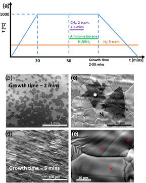
Figure 2. Synthesis of large ultra-thin h-BN films by a methane-assisted approach. (a) Growth conditions used in this experiments. AB stands for ammonia borane. (b) and (c) SEM images of isolated and large domains after 2 min growth. (d) and (e) Continuous ultra-thin films after 5 min growth.
Download figure:
Standard image High-resolution imageCharacterization of single- and few- layer h-BN by Raman spectroscopy over large areas (mapping) has been difficult due to the low intensity of the h-BN signal, in contrast to graphene. Because of this shortcoming, other methods need to be used to detect and map the number of layers of h-BN films. In order to determine the thickness and crystallinity of our h-BN films we used low-energy electron microscopy (LEEM). This method has been extensively used to determine the number of layers for both graphene [37–39] and h-BN [34, 40], by examining the low-energy electron reflectivity (LEER) spectra. Here, we used LEEM to map h-BN thickness over the Ni surface, as shown in figure 3. A typical LEEM image is shown in figure 3(a), with figure 3(b) showing a map of the number of layers (blue-1 layer, red-2 layers), extracted from the LEER spectra displayed in figure 3(c). LEER spectra are recorded at every pixel within the image of figure 3(a), and figure 3(c) displays some of these spectra. In such spectra, reflectivity minima occur at energies of specific electronic states of the system; the spectra thus provide a 'fingerprint' of the atomic arrangements on the surface [34]. Considering first the spectra at locations C and D, these are characterized by distinct reflectivity minima at about 3 eV and at 8–9 eV. The 3 eV minimum arises from an interlayer electronic state that occurs between two layers of h-BN, whereas the 8–9 eV minimum is associated with electronic states that occur on the h-BN planes (as opposed to between the planes) [34]. Thus, these two spectra definitely establish the presence of two h-BN layers on the surface at these locations. Moving to the spectrum at location B, the higher energy minimum near 8 eV is still present, but the lower energy one at 3 eV is absent. Thus, this type of spectrum definitively establishes the presence of only a single h-BN layer [34]. Finally, for the spectrum at location A in figure 3(a), we see some features reminiscent of spectrum B in figure 3(c), but at the same time the intensity of the reflectivity above 8 eV is significantly reduced. This type of curve is not typical of the ones that we generally obtain for these surfaces, and its interpretation is not completely clear. It appears that there is little, if any h-BN in this region of the surface, and indeed, spectrum A is somewhat similar to those that we have observed on bare metal surfaces [38]. Tentatively, we assign the location A and surrounding area to 0 ml of h-BN. By analyzing the spectra from each point in figure 3(a), the map shown in figure 3(b) was obtained [41]. Several samples and areas were tested using this method and the results were consistent, i.e. large-areas were covered with 1 and 2 layers of h-BN.
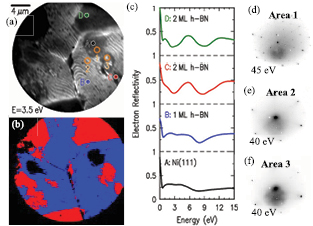
Figure 3. LEEM and µLEED characterization. (a) LEEM image of h-BN/Ni. (b) LEEM map of h-BN thickness, showing the presence of one and two h-BN layers as determined from the spectra in (c) at each point over the film surface in the field of view. Blue and red denote single-layer and double-layer h-BN, respectively. (c) A series of reflectivity spectra from different points in (a), from A to D. In C and D, two reflectivity minima are observed near 3 and at 8–9 eV, indicative of 2 ML h-BN. In B, only a single minimum near 8 eV is found, indicative of 1 ML h-BN. For spectrum A, no distinct minima are observed, and tentatively the spectrum is assigned to little or no h-BN on the surface. (d)–(f) µLEED images from area 1, 2 and 3 in (a). Area 1 is bare Ni (1 1 1); it is apparent that the diffraction points of the h-BN from areas 2 and 3 overlap with those of the Ni (1 1 1).
Download figure:
Standard image High-resolution imageFigures 3(d)–(f) show selected-area LEED (µLEED) patterns, obtained from the areas indicated in (a). Based on the LEER spectra, area 1 contains little if any h-BN, area 2 contains 1 ml of h-BN, and area 3 contains 2 ml of h-BN. The LEED patterns of areas 2 and 3 are seen to contain six primary spots in a hexagonal arrangement; these spots arise from the h-BN on the surface. For the pattern from area 1, six spots at the same locations of those of areas 2 and 3 can again be seen, but many additional spots are also seen. Based on the LEER spectrum indicating  h-BN coverage in this area, we assign this pattern to bare Ni, and from its hexagonal arrangement we deduce that the Ni surface has a (1 1 1) orientation. The fact that the six diffraction spots in areas 2 and 3 are aligned with those of area 1 indicates that the h-BN is aligned with the underlying nickel [34]. Figures S6 and S7 contain additional LEEM and µLEED data.
Growth mechanism
The h-BN growth was carried out in an ammonia–borane partial pressures of 10–100 mTorr where the pressure was controlled by heating the precursor to a specific temperature to control the evaporation rate. We found that in order to obtain h-BN on the interior surface of the enclosure (with carbon present), a minimum chamber ammonia–borane partial pressure of ~50 mTorr was needed. Below this pressure no h-BN was observed. As mentioned above, the minimum pressure of the growth system is ~8 mTorr. At this base pressure the oxygen partial pressure in the chamber is significant and needs to be taken in consideration as it can oxidize the surface of the Ni, potentially forming a uniform layer of NiOx on the surface. The ammonia–borane is introduced into the chamber at ~50 mTorr partial pressure immediately after annealing the Ni in hydrogen as shown schematically figure 2(a). The thermal decomposition of the ammonia–borane on the surface of NiOx/Ni is a complex process involving various thermal reduction and dehydrogenation steps [42], leading eventually to the formation of h-BN. In the case of carbon-free growth, the B and N species reach the surface of the Ni (flat substrates and exterior of the enclosure) where the B-containing compounds are believed to react with the NiOx leading to the formation of B2O3 as shown by the XPS spectra in figure 5. The formation of boron oxide was already observed in our previous report on flat substrates [15]. The rest of the B species react with the N species to form the h-BN film. However, inside an enclosure, we hypothesize, that the amount of precursor that diffuses through the small apertures in the mechanically folded enclosure is significantly lower, and the degree of Ni oxidation is most likely higher due to the trapped air, in comparison to the exterior surface. This is similar to the case of the CVD of graphene using Cu enclosures [3], where it was shown that the oxidation of the surface decreased the density of nuclei which led to large area graphene single crystals [3]. Such a model is consistent with the kinetic theory of gases where a small gap in the enclosure (relative to the interior surface area) impacts the mass flow, and diffusion rate [13], of the precursor and other vapor phase compounds into the enclosure. In order to shed light on potential intermediate reactions of the precursors with the oxidized Ni surface, free energy of formation calculations were performed. Figure 4 shows a summary of such calculations plotted as a function of temperature (see supporting information for calculation details). Figure 4(a) represents the free-energy of formation as a function of temperature for boron and nickel oxides. It can be seen that the B2O3 phase is thermodynamically preferable over NiO as shown for various potential chemical reactions in the CVD process. Figure 4(b) shows a similar plot but for the BN phase formation, comparing reactions with and without carbon. These calculations suggest that, in the presence of carbon, the free-energy of formation of the BN phase is more negative, i.e. thermodynamically more favorable. This supports our data that indicate the formation of ultra-thin h-BN layers in the presence of carbon. It should be noted that NH3 in a similar way as CH4 should also reduce the B2O3 to form BN. In our experiments, however, the ammonia-assisted growth led only to the partial formation of multi-layer and non-homogeneous h-BN domains (figure S1). Also important to note, from the Ellingham diagram, is that B2O3 cannot be reduced by annealing in H2 at the growth temperatures used in this work (figure S10). Thus, the introduction of small amounts (~1 mg) of amorphous carbon into the enclosure or a few sccm (up to 5) of methane flow, while exposing the Ni surface to the ammonia–borane, leads to h-BN growth by a reduction of boron oxide by a carbo-thermal process [29, 43, 44].

Figure 4. (a) Thermodynamic calculations for B and Ni oxidation and (b) for the formation of the BN phase. In both, the inset in red margins is an expansion of the larger graph around the growth temperature (~1273 K). The potential chemical reactions are shown below each graph.
Download figure:
Standard image High-resolution image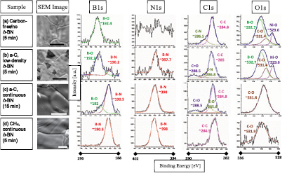
Figure 5. XPS Characterization. Every row shows the result for a different sample in which a representative SEM image of the interior of the enclosure is shown in (a)–(d): (a) carbon-free (no h-BN—10 min growth), (b) a-C (low density h-BN domain area—5 min growth), (c) a-C (continuous h-BN film area—15 min growth) and (d) CH4-assisted growth (continuous h-BN film—5 min growth). Scale bars are 50 µm for (a) and (b), 10 µm in (c) and (d). The columns for the XPS spectra regions from left.
Download figure:
Standard image High-resolution imageEx situ XPS and ToF-SIMS chemical characterization were also used to support our results and the growth mechanism. Figure 5 shows the SEM images and XPS spectra of four different samples (all four taken from the interior surface of the Ni enclosures). Figure 5 summarizes the data for 4 different experiments, each column contains the data of a different sample and every row contains the data acquired for the B1s, N1s, C1s and O1s core levels, from top to bottom. Comparing the B1s spectra of the different samples, it is evident that the B–O phase is present in all of the samples except for the CH4-assisted growth. It should be noted that in the carbon-free sample, the B1s peak is associated with the B–O binding energy (Eb = 192.4 eV, which corresponds to the B2O3) [45, 46], and correlates with the lack of h-BN on these samples. The contribution of the B–O phase to the B1s peak decreases with increasing h-BN quality and coverage. Similarly, the N1s peak intensity increases with the h-BN coverage (from top to bottom). We note that the amount of carbon present on the sample surface, as indicated by the C1s peak area, is reduced with the coverage of h-BN and the use of amorphous carbon or methane, figure S11. This suggests that the carbon used to aid the B2O3 reduction is not incorporated into the h-BN lattice. This conclusion is supported by the absence of a graphitic signal in the Raman spectra, figures S2–S4. In addition, a reduction of the oxygen content is observed with increasing coverage and quality of the h-BN layer (figure S11). Analysis of the relative amounts of carbon and oxygen are shown in figure S11, calculated from the respective peak areas.
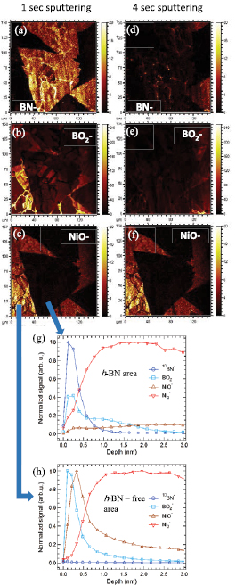
To corroborate the above results, we used ToF-SIMS, an ultra-high chemical and surface sensitive technique [47, 48] which has a high lateral resolution (~200 nm) and enables chemical mapping. Figures 6(a)–(c) show the chemical maps for BN−,  and NiO− ions respectively after ~1 s of Cs+ sputtering (~0.1 nm depth) to clean the surface of adsorbates. Hexagonal BN triangular domains are observed in figure 6(a), where the
  and NiO− distributions are spatially separated from the h-BN covered areas. The ToF-SIMS data further support the growth mechanism, that is, NiOx is reduced by B species to form B2O3 which is further reduced by C (or CHx) and N species to form h-BN and thus leading to a lower concentration of B2O3 and NiOx species underneath the h-BN (brighter color indicates a higher concentration). Figures 6(d)–(f) show the same elemental mapping but after sputtering for 4 s (at ~0.6 nm depth), which completely removed the h-BN and the B2O3 layer. The NiOx on the other hand, seems to be thicker in the h-BN-free regions (~2 nm) and it took about 10 s to remove it, (figures S12 and S13). The depth conversion [48, 49] of the Cs+ sputtering time is shown in figures 6(g), (h) and S12, where each data point represents 1 s of Cs+ sputtering. The ToF-SIMS analysis shows that B2O3 is on the surface and is removed by 4 s of sputtering, <1 nm thick. This appears to be crucial for the formation of ultra-thin h-BN (1 and 2 layers as shown by LEEM measurements), as it inhibits the diffusion of the B (and N) into the Ni, as demonstrated previously [12–15, 35]. This suggests that the B-assisted reduction of NiOx and the subsequent formation of B2O3 fixes the B atoms at the surface of the metal until the h-BN is formed. Figures 6(g) and (h) show profiles from h-BN and h-BN-free areas supporting this analysis. However, further experiments are needed to understand the reason and mechanism for the formation of a bi-layer, as detected in the LEEM results. As mentioned above, we also evaluated the effect of ammonia gas instead of carbon (amorphous or methane) as a possible B2O3 reducing agent [50] to form h-BN and indeed it was detected inside the Ni enclosures despite the lack of carbon (figure S1). However, the h-BN grown using NH3 was not continuous for the conditions that we used. Further experiments are needed to understand the differences between carbon- and ammonia-assisted h-BN growth, indeed there are competing reactions occurring in the system, each with complex rate coefficients.
Figure 6. TOF-SIMS characterization. (a)–(c) Maps of the BN−,  and NiO− secondary ions, after 1 s of Cs+ sputtering (~0.1 nm depth) to clean the surface. (d)–(f) Same location maps of the same ions after 4 s of Cs+ sputtering (~0.6 nm depth), showing that the BN and boron oxide layers were sputtered away, (d) and (e) show that BN and boron oxide layers are completely removed, in contrast to the Ni oxide layer which needed about 10 s of Cs+ sputtering (~2 nm depth) to be completely removed (figure S12). (g) and (h) Show profiles of the relevant ions for h-BN and h-BN-free areas, respectively. Scan size in all the cases are 150 µm2.
Download figure:
Standard image High-resolution image
We have demonstrated the synthesis of ultra-thin h-BN films composed of 1 and 2 layers with large-domains by carbon assisted-growth in the interior of a Ni enclosure. The h-BN films were characterized by LEEM and µLEED. The formation the mono- and bi-layer h-BN, in contrast to the growth of thick h-BN on Ni and Co foils [12, 15], is explained by an intermediate formation of boron oxide on the interior of the enclosures which inhibits the diffusion of B and N into the bulk of the metal. The boron oxide is then reduced using carbon in the form of amorphous carbon or CH4 gas leaving the B to react with the NH3 thus forming h-BN. Ex situ XPS and ToF-SIMS were performed to identify boron oxide in h-BN free areas/samples. In the case of a fully covered Ni surface with h-BN, boron oxide was not observed.
The results presented in this paper emphasize the importance of having a basic understanding and control of the growth environment in h-BN growth by CVD. We also show that controlled layer growth of h-BN on Ni (or other metals) can be achieved by a suitable metal surface chemical modification. Further experiments and calculations are needed in order to fully understand the influence of the crystal orientation of the Ni on such a growth process. In principle, by carefully controlling the growth system ambient chemistry, the same results could be obtained on flat surfaces.
Experimental
h-BN growth
Three different types of samples were tested in this work: (1) flat Ni foils, (2) flat Ni thin films and (3) Ni foil enclosures. The incorporation of carbon to the system was achieved by adding ~1 mg of amorphous carbon (99% 13C enriched amorphous carbon powder was used, Cambridge Isotope Laboratories, Inc. CLM-402-1) to the Ni enclosures or by flowing CH4 (~1–5 sccm, 99.999%, Airgas). The synthesis of h-BN was carried out by LPCVD as reported previously [15]. Briefly, the growth substrate was placed in the center of a 1 inch diameter quartz tube, which was placed in a tube furnace. The chamber was then evacuated to ~8 mTorr base pressure. Hydrogen (10 sccm, 99.999%, Airgas) was then flowed through the system. The sample was heated to the growth temperature (typically 1000–1050 °C) and the sample was annealed at such conditions for 30 min. Thereafter, the hydrogen flow was reduced to 5 sccm and the ammonia–borane was independently heated to 80–100 °C to produce the desired partial pressure of ammonia–borane; the partial pressure of ammonia–borane was monitored to be around 60 mTorr. The growth was performed for times ranging between 5 and 30 min.
Characterization
Optical microscopy (OM): bright and dark field, Zeiss Axiovert 100A Light Microscope.
Scanning electron microscopy (SEM): FEI Quanta-600
Transmission electron microscopy (TEM): JEOL 2100-F 200 kV Field—with silicon nitride coated copper grids, Ted Pella, 215365.
Raman spectroscopy (RS): Witec Alpha 300 micro-Raman confocal microscope.
X-ray photoelectron spectroscopy (XPS): was conducted using a commercial x-ray photoelectron spectrometer (Kratos Axis Ultra), using a monochromated Al Kα x-ray source (hν = 1486.7 eV), electrostatic lens optics, and a multichannel plate and delay line detector coupled to a hemispherical analyzer (180° with a 165 mm mean radius). The photoelectron takeoff angle was normal to the surface of the sample and 45° with respect to the x-ray beam. High-resolution spectra were collected with a pass energy of 20 eV. The pressure in the analysis chamber was typically 2 × 10⁻⁹ Torr during data acquisition.
Scanning tunneling microscopy (STM): The sample was loaded into an ultra-high vacuum (UHV) surface analysis system with a base pressure in low 1 × 10⁻¹⁰ mbar range described elsewhere [51, 52]. The h-BN surface was imaged using an Omicron variable temperature STM without any thermal treatment. The STM images were obtained at room temperature and in the constant-current mode, with an etched tungsten tip.
Time-of-flight secondary ion mass spectrometry (ToF-SIMS): The ToF-SIMS data were collected with a commercial ION-ToF SIMS 5 instrument which was configured in the high-resolution burst alignment (BA) mode that enabled mapping at ~200 nm lateral resolution. The samples were probed with a 30 keV Bi + analysis ion beam (18 ns burst pulse duration) and a 1 keV Cs + sputter beam (~55 nA sample current), which were raster scanned over areas of 150 × 150 µm2 and 250 × 250 µm2, respectively. The Cs + sputtering rates were calculated at ~0.12 nm s−1 and 0.22 nm s−1 for h-BN and Ni, respectively. All spectra were collected in negative polarity with a mass resolution > 5000 (m/δm) at a base pressure <2 × 10⁻⁹ Torr.
Low-energy electron microscopy (LEEM): We performed LEEM and selected-area µLEED in an Elmitec LEEM III. In this apparatus, incident and reflected/diffracted electrons are separated from one another by a 60° magnetic beam splitter. All LEEM images here were acquired in bright-field mode, wherein the electron-beam is momentum filtered such that only secularly reflected electrons participate in image formation. By obtaining many such images at different incident electron energies, we then extract LEER spectra from given points on the surface. These experimental spectra are then compared to a first-principles method for describing LEER which has been described elsewhere [37–39]. µLEED is performed by the introduction of a collimating aperture which restricts the size of the electron beam to ~1 µm in diameter, allowing us to locally probe the crystallinity across the surface.
Acknowledgment
AI acknowledges support from the Israel Science Foundation, project number 1784/15. RSR was supported in part by the Institute for Basic Science (IBS-R019-D1). The work at The University of Texas at Austin (UTA) was supported by the Keck Foundation grant no. 749046 and the Department of Defense—Navy grant N00014-10-1-0254. We also acknowledge the NSF grant DMR-0923096 used to purchase the TOF-SIMS instrument at Texas Materials Institute, UTA. Material synthesis and characterization was also supported by the South West Academy of Nanoelectronics (SWAN 2.0, grant 2013-NE-2400) and the Center for Low Energy Systems Technology (LEAST), one of the six centers supported by the STARnet phase of the Focus Center Research Program, a Semiconductor Research Corporation program sponsored by MARCO and DARPA. Work at the Molecular Foundry was supported by the Office of Science, Office of Basic Energy Sciences, of the U.S. Department of Energy under Contract No. DE-AC02-05CH11231.
Associated content
Supporting Information. The supporting information includes additional LEEM and µLEED data, energy of formation calculations for the different oxide phases and the CH4-assisted growth results, TOF-SIMS mapping and depth profiling, Raman spectroscopy and mapping of h-BN ad-layers.
Author contributions
The manuscript was written through contributions of all authors./All authors have given approval to the final version of the manuscript.