

Abstract
The synthesis of graphene nanoislands with tailored quantum properties requires an atomic control of the morphology and crystal structure. As one reduces their size down to the nanometer scale, domain boundary and edge energetics, as well as nucleation and growth mechanisms impose different stability and kinetic landscape from that at the microscale. This offers the possibility to synthesize structures that are exclusive to the nanoscale, but also calls for fundamental growth studies in order to control them.
By employing high-resolution scanning tunneling microscopy we elucidate the atomic stacking configurations, domain boundaries, and edge structure of graphene nanoislands grown on Ni(1 1 1) by CVD and post-annealed at different temperatures. We find a non-conventional multistep mechanism that separates the thermal regimes for growth, edge reconstruction, and final stacking configuration, leading to nanoisland morphologies that are incompatible with their stacking symmetry. Whole islands shift their stacking configuration during cooling down, and others present continuous transitions at the edges. A statistical analysis of the domain structures obtained at different annealing temperatures reveals how polycrystalline, ill-defined structures heal into shape-selected islands of a single predominant stacking. The high crystallinity and the control on morphology and edge structure makes these graphene nanoislands ideal for their application in optoelectronics and spintronics.
Export citation and abstract BibTeX RIS
1. Introduction
Scaling down graphene to the nanoscale is an efficient route to tune its quantum properties. Depending on the edge structure one can induce size-dependent energy gaps [1–3] that tune the optical and plasmonic response [4, 5], or emerging phenomena such as 1D edge magnetism [6, 7] and spin filtering [8]. Although top-down lithographic techniques have successfully been employed to produce graphene nanostructures down to the scale of ∼5–20 nm, they exhibit chemically and structurally disordered edges [9], and the corresponding energy gaps below 10–100 meV are insufficient for room temperature applications [2]. Bottom-up on-surface chemistry, on the other hand, offers a promising alternative to produce sub-10 nm nanoribbons and nanoislands with well-defined edge and crystalline structure [10–12].
In particular, nanoscale graphene islands can be synthesized on different metallic substrates by CVD [11–16]. However, the precise structural control will depend on the reactivity and epitaxial interaction of the underlying surface. The lattice symmetry and mismatch of the substrate will define the morphology [17–19], and stabilize armchair [20], zigzag [21–23], or reconstructed [12, 23–25] edges. In this respect the Ni(1 1 1) surface, with a mismatch of 1.2 , represents an ideal candidate that can lead to triangular and hexagonal islands combining zigzag and reconstructed edges [11, 23].
The final electronic properties will not only be affected by the morphology and edge structure, but also by the internal grain distribution and boundary structure [26–30]. Domain boundaries in epitaxial graphene can be made of topological defects, or represent a strained stacking transition of the honeycomb lattice [31]. The two will have very different consequences on the electronic properties of the nanoislands after transferring them out of the catalytic metallic template, as required by most applications. Topological defects are prone to perturb transport properties by inducing gaps [26], 1D conducting channels [32, 33], or by more subtle valley filtering mechanisms [34]. The defects, and hence the above mentioned phenomena, will persist once the nanoislands are transferred to insulating templates. On the other hand, strained boundaries that separate two non-rotated stacking domains will vanish once we separate the nanoisland from the underlying metallic template.
Controlling stacking configurations and domain boundary and edge structures of graphene nanoislands is therefore of primary relevance. In this study we show that by varying the final post-annealing temperature in a two-step CVD method, islands of different morphology and crystalline structure can be obtained. The lowest annealing temperatures give rise to irregular island morphologies and polycrystalline structures that could host quantum dots and metallic 1D boundaries. In addition, we find a multiple step mechanism that consists on (i) growth at top-fcc stacking, followed by (ii) edge reconstruction, and (iii) displacement to bridge-top stacking during cooling down, which leads to morphologies and edge structures that are not consistent with the stacking symmetry. Finally, increasing the annealing temperature leads to a structural healing and the formation of single-domain top-fcc islands of well-defined shape and edge structure. The results are relevant not only for the synthesis of nanoislands with tailored optoelectronic and magnetic properties, but also for the understanding of grain boundary structures on extended polycrystalline graphene, which play a crucial role in charge and spin transport [28, 35].
2. Methods
2.1. Synthesis and characterization
The Ni(1 1 1) single-crystal has been prepared by Ar+ sputtering (1 kV, 15 min) and annealing (700 °C, 5 min) cycles. The graphene nanoislands were grown on the clean Ni surface by following a temperature programmed procedure that consists on : (i) a room temperature dose of the precursor gas (ethylene or propene), exposing  mbar for ca. 5 min; (ii) evacuation of the precursor to recover initial UHV conditions; (iii) a first step annealing of 5 to 8 min to 500 °C for the nucleation of structurally disordered islands; (iii) a second step annealing of 5–10 min at different temperatures for their structural modification [11, 23]. We explore the post-annealing temperature range of 500–620 °C, which basically defines the stability range of graphene on Ni, with carbide formation below and bulk diffusion of C above [11, 36].
The morphology and stacking configuration of the nanoislands were characterized in situ without breaking the vacuum conditions by scanning tunneling microscopy (STM) performed at room temperature.
2.2. Analysis of stacking configurations
The strong interaction between graphene and metals such as Ni results in local electronic perturbations that distort the honeycomb lattice appearance in STM topographic images. In top-hollow stacking configuration for instance, only sublattice atoms in hollow sites are imaged as protrusions [11, 23, 31, 37, 38]. However, the assignment of a particular appearance to a stacking configuration is not straightforward, it depends on tunneling conditions and the chemical state of the tip, and it relies on comparison to theoretical simulations [31].
In this work, we acquire high resolution images that resolve the atomic lattice of both the graphene and surrounding Ni surface. An extrapolated Ni lattice is superimposed to the graphene islands to determine stacking configurations from the relative graphene-Ni lattice positions instead of relying on the STM appearance. Thermal drift and piezocapacitance distortions are compensated by linear transformations until the Ni lattice is matched with a single hexagonal grid within the whole image, assuring a correct Ni lattice extrapolation under the graphene islands (see supplementary information (stacks.iop.org/TDM/4/025104/mmedia)). This allows us to identify the atomic stacking sites of all C atoms in the image. The two hollow sites, namely fcc and hcp, are differentiated by assuming the predominance of top-fcc stacking, as found by both theoretical and experimental studies of extended graphene on Ni(1 1 1) [31, 39–42].
3. Results and discussion
A representative example of graphene nanoislands obtained at an intermediate post-annealing temperature of 525–575 °C is shown in the STM topographic images of figure 1. The characteristic region of the samples we studied are presented in figure 1(a), with monodisperse and coalesced islands of different size varying from 5–100 nm2. Figure 1(b) is a high-resolution image of a single island comprising all the features we will discuss in this study: stacking domains separated by either strained or sharp topological defect boundaries, and conventional and reconstructed zig-zag edges.
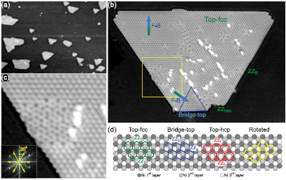
Figure 1. (a) Representative overview and (b) multidomain island obtained by post-annealing at 525 °C and 575 °C respectively. In the latter, one can observe: (i) small rotated domains surrounded by a top-fcc stacking matrix (example highlighted by a yellow square); (ii) regions where the stacking gradually changes to bridge-top (green-blue arrows); (iii) conventional  (zzh) and
  reconstructed (zzrec) zig–zag edges corresponding to hollow and top stacking terminations respectively. Image size and tunneling conditions from left to right, grouped as (size, It, Vb): (
 nm2, 0.19 nA, 650 mV), and (
 nm2, 22 nA, 78 mV). (c) Zoom of the yellow square in (b). The inset is the FFT of the same image revealing the two lattices with 30° of relative rotation. (d) Schematic representation of the four stacking configurations observed.
Download figure:
Standard image High-resolution image3.1. Stacking domains
Four different stacking configurations have been identified by employing drift-corrected, atomically resolved images with a superimposed Ni lattice grid (see supplementary information), which are schematically represented in figure 1(d): top-fcc, top-hcp, bridge-top, and a set of domains with a range of azimuthal rotation angles relative to the other three, called rotated domains hereafter. An example of the latter is shown in the zoomed image of figure 1(c), and the relative angle with respect to the top-fcc stacking can be obtained from the corresponding reciprocal lattices in the Fourier transform (FFT) image (see inset). Each of these stacking domains have been already observed in extended graphene layers grown on Ni(1 1 1) in different conditions [31, 32, 39, 40, 43].
Rotated domains are the easiest to identify. With finite azimuthal rotation relative to the underlying substrate, they give rise to short periodicity Moiré patterns that can be clearly distinguished (see figure 1(c)). They only appear embedded in multidomain islands, never as individual islands, and represent a structural discontinuity with respect to the non-rotated matrix.
As opposed to rotated domains, top-fcc, top-hcp, and bridge-top stackings are in coherent registry with the underlying Ni lattice, with all atoms of each sublattice at the same site and no relative rotation (see atomic sketches in figure 1(d)). The three stacking configurations can appear either coexisting in multidomain islands (see, e.g. figure 4) or, if the island is small enough or the temperature high enough, as single-domain islands. In all cases top-fcc domains are clearly predominant, with bridge-top domains appearing in second place.
3.2. Equilibrium and stacking symmetry forbidden morphologies in single domain islands
Single-domain islands enable the study of edge structures and the equilibrium shapes that are determined by their energetics and growth kinetics. Examples of each non-rotated stacking configuration are displayed in figure 2. Their different registry with the underlying Ni atoms can be tracked down in the zoomed images containing both superimposed Ni and graphene lattices.
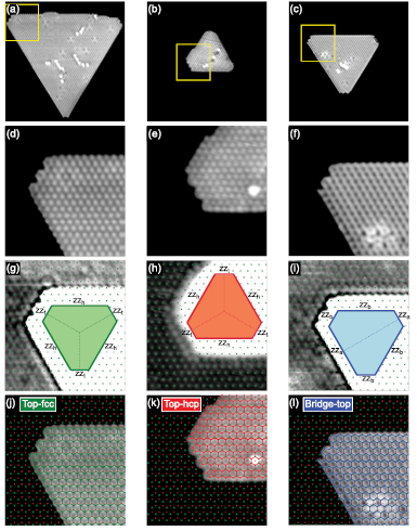
Figure 2. Graphene islands of top-fcc (a), top-hcp (b), and bridge-top (c) stacking. By adjusting brightness and contrast we show either the graphene structures (d)–(f) or the underling Ni atoms (g)–(i) in the zoomed areas indicated in (a)–(c). The dashed lines in the truncated triangles of (g)–(i) indicate the symmetry of the corresponding zigzag edges. In (j)–(l) we superimpose the Ni and graphene lattices (see supplementary information). Green crosses (red F) represent the Ni top (fcc) sites. Image size:  nm2 and
  nm2 for large and zoomed images respectively. Post-annealing temperature and tunneling conditions from left to right, grouped as (T, It, Vb): (575 °C, 16 nA, 83 mV), (560 °C, 10 nA, 24 mV), (575 °C, 15 nA, 83 mV).
Download figure:
Standard image High-resolution imageFor top-fcc and top-hcp islands, the three-fold stacking symmetry of their edges can account for the observed truncated triangular shape. Similar to graphene in other metals, their most stable edge orientation on Ni(1 1 1) is the zig-zag [12, 21, 22], and the stacking symmetry groups them in two sets of three equivalent edges according to their hollow (zzh) and top (zzt) site (see schematic triangles of figures 2(g) and (h), and figure 3(a)). The opposing direction of top-fcc and top-hcp islands derives from the 60° rotation relation of their respective zzh and zzt edges. In both cases, the long edges correspond to zzh, the most stable edge structure according to DFT calculations [12, 23]. The shorter truncated edges, on the other hand, run along the highly unstable zig-zag directions with top stacking, which minimize their energy by undergoing different reconstructions. Recent studies indicate that, at the growth temperature of 470 °C, zzt edges exhibit a Klein structure, with additional C atoms attached to the zig-zag edge atom [25]. At room temperature, on the other hand, different types of  superstructures have been proposed, depending on the experimental conditions. DFT calculations indicate that Hydrogen passivation tends to pair the Klein edge atoms [25], whereas the most stable reconstruction in the absence of Hydrogen consists on pentagon-heptagon units [23]. The two superstructures give rise to very similar topographic appearance, impeding the identification of the exact structure solely from STM images (see supplementary information). Yet, the fact that zzh edges are imaged at the same apparent height as the inner C lattice indicates that edge atoms might be H-passivated rather than tilted down and coordinated with Ni surface atoms [25], suggesting that the superstructure we observe in the truncated edges is the passivated
  Klein.
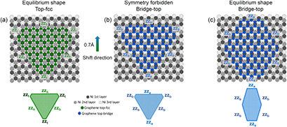
Figure 3. Schematic representation of the atomic stacking of top-fcc (a) and bridge-top (b) triangular islands. The two are connected by a translation of 0.7  perpendicular to a zig-zag edge. According to the stacking symmetry of edges, this morphology can only correspond to top-fcc islands. (c) Equilibrium morphology of bridge-top islands, for the case of zzb being more stable than zza.
Download figure:
Standard image High-resolution imageIn contrast to top-hollow islands, the triangular shape of the bridge-top islands that we find is not at all compatible with the two-fold stacking symmetry of its edges (see the atomic representations of figures 3(b) and (c)). Bridge-top islands with zig-zag termination exhibit one pair of opposing a-type (zza), and two pairs of opposing b-type (zzb) edges, which should give rise to uniaxially elongated or compressed hexagonal shapes depending on their relative energy. This statement, solely based on symmetric arguments and applicable both in the kinetically limited and equilibrium growth regimes, is however in stark contrast to the experimentally observed triangles. We attribute the origin of this non-equilibrium morphology to substantial differences in the stacking energetics at growth and room temperature. The triangular shape and orientation of the bridge-top island of figure 2(i), together with the  reconstruction of the truncated edges, suggest that the stacking configuration at the growth temperature is top-fcc, and hence must have been shifted to bridge-top during cooling. This scenario is supported by recent DFT calculations that reveal an isoenergetic path connecting top-fcc and bridge-top configurations by a 0.7
  translation along the armchair direction [42]. A shift of an entire island from top-fcc to bridge-top with such a translation is depicted in figures 3(a) and (b), revealing a change from three- to two-fold stacking symmetry.
The truncated edge structure of bridge-top islands can provide some information about the relative kinetics of the two different processes that occur during the cool down: the shift to bridge-top stacking, and the reconstruction of zzt truncated edges. The latter will only take place if the stacking shift has not occurred before, since reconstruction is directly related to the highly unstable top stacking of edge atoms. The fact that some bridge top islands do exhibit unreconstructed truncated edges reveal, however, that edge reconstruction can under certain conditions be kinetically inhibited (see, e.g. the top edge of the island in figure 4(a)).
3.3. Stacking domain boundaries
We start discussing the case of non-rotated domains, where both strained and topological defect boundaries can exist, as illustrated with the examples of figure 4. The two triangular islands of figure 4(a) are fused by two type of topological boundaries: on the left side, a stripe of rotated domain bridges the two islands by the corresponding topological boundaries. Boundaries of this type, formed around rotated domains will be discussed later. On the right side, the two islands are directly connected by a topological line defect (see bottom image of figure 4(a)). This type of topological boundary, consisting on an alternating pair of pentagons and an octagon (558) has already been observed in extended graphene separating top-fcc and top-hcp domains [32]. In our case, the bottom island is top-fcc, and the top island seems to have grown as top-hcp based on its triangular shape and orientation, and later shift to bridge-top during cooling. The seldom 558 boundaries that we find are always zipping two non-rotated, well-defined islands, indicating that the boundary has been created during the coalescence of individual islands.
Continuous strained top-fcc/bridge-top boundaries are more ubiquitous. They appear always as peripheral domains and do not show any signature of coalescence. Instead, they seem to be more related to the stacking shift of a region occurring during cooling, similar to that observed in single-domain islands. From our stacking analysis we find that such boundaries consist on continuously strained regions (see bottom image of figure 4(b)). Top-fcc/bridge-top strain boundaries have already been observed in extended graphene grown on Ni(1 1 1) [31], and interpreted in terms of a shear strain along the zigzag direction. In the nanoislands, however, we find tensile strain boundaries, as shown in the zoomed section of figure 4(b). The selection of strain direction seems to be related to the interplay between strain and edge energetics, as discussed below.
A peculiar characteristic of the bridge-top stacking is that the orientation of edge types is not univocal, and will depend on the shift direction, and thus the corresponding strain direction at the boundary. In domains with continuous boundaries, a tensile distortion of 0.7  perpendicular to the zzh edge leads to zza edges (see the zoomed image of figure 4(b)). The more favourable zzb edge requires an unrealistic compressive strain of more than one hexagonal unit cell, or a combined 0.6
  shear and a 0.4
  compressive distortions, both less favourable than the observed tensile strain. Regarding the topological 558 boundary of the island in figure 4(a), this is also distorted due to the stacking shift of the original top-hcp domain to bridge-top. The corresponding distortion of the pentagon and octagon edges with respect to the axially symmetric top-fcc/top-hcp boundaries (see figure S16 in supplementary information) reveals a shear strain, in spite of this implying less energetically favourable edge structures than by applying an axial strain, where both long edges would correspond to the zzb type. The two cases indicate that it is the boundary energetics that determines the shifting direction rather than edge energetics.

Figure 4. Top-fcc/bridge-top stacking domain boundaries. (a) A top-fcc and a bridge-top island merged by a rotated domain on the left, and a 558 topological defect line on the right. A zoom of the latter is shown at the bottom, with the superimposed Ni and graphene lattices obtained from the analysis (see supplementary information). Here green crosses and red F's represent the Ni top and fcc sites respectively. (b) A multidomain island with continuous top-fcc to bridge-top boundaries. The longest edges of the latter are always of zza type. The continuous mismatch between the graphene and Ni lattices in the strained transition regime can be seen in the zoomed image at the bottom, where both lattices are superimposed. Post-annealing temperature and tunneling conditions grouped as (T, It, Vb): (a) (575 °C, 15 nA, 83 mV); (b) (560 °C, 14 nA, 22 mV).
Download figure:
Standard image High-resolution imageRegarding top-hcp domains, the seldom ones we find are predominantly small triangular monodomain islands as the one shown in figure 2(b). Only occasional multidomain islands contain top-hcp domains, the latter exhibiting continuous strained boundaries with both top-fcc and bridge-top domains, similar to top-fcc/bridge-top continuous boundaries (see figure S15 in supplementary information).
As opposed to non-rotated stacking domains, domains with relative rotation can only be interfaced by topological defect boundaries. The minimum energy ones have been described in theoretical studies by periodic arrays of pentagon-heptagon (57) pairs in different configurations [44–47]. The calculated angle-dependent energetics predicts a metastable plateau spanning around 20–35° with a particular pronounced minimum around 28–32°, related to C–C bond relaxation around the topological defect.
We compare our experimental results to the above predictions by analysing the relative angle between the lattices of rotated and top-fcc domains. We do that using the atomic resolution of real space images. Figure 5(a) shows an example of such analysis and the resulting statistics of the angular distribution. Interestingly, all observed domains fall within the calculated metastable region [44, 46, 47]. We never observe small-angle rotation domains (<15°), as have been found for instance in extended CVD graphene on Cu foils [48]. The inhibition of small-angle domains could reflect the decisive role in Ni of the stacking energetics in this regime. At intermediate angles, however, boundary energetics seems to dominate, according to the coincidence of our statistical distribution with the free standing calculations. This coincidence is in contrast with the distribution found in extended graphene, where the peak at 17° cannot be related to any energetic minimum of free-standing boundaries [49].

Figure 5. (a) Example of an island used in the analysis of rotated domains. The colored regions correspond to different stacking domains (green is top-fcc, others are rotated domains with different angles). (b) Statistical distribution of rotated angles. (c) and (e) Well-defined 30° rotated domains. (c) Linear ribbon with type I boundary. Yellow/green arrows indicate the translation vectors of the boundary at each side and the white arrow the coincident Moiré periodicity. (d) The Moiré pattern of a 30° rotated domain, with the (1, 3) translation vector. (e) Quantum dot with type II boundary. (f) Irregular rotated domain combining type I and type II boundaries.
Download figure:
Standard image High-resolution imageThe pronounced maximum at 30° agrees very well with the local stability maximum predicted around this angle. Several arrangements of 57 units have been proposed for this angle [44–47]. Atomically resolved images as the ones displayed in figures 5(c), (e) and (f) are representative of the boundaries we find, always made of continuous 57 arrays7. Type I boundaries are linear and define ribbons of the rotated stacking domain, whereas the type II structure form quantum dots. Most domains, however, are limited by less symmetric boundaries that combine both types (see figure 5(f)).

Figure 6. Evolution of stacking domains with annealing temperature. (a) Domain size and (b) relative abundance. (c) Representative images of the thermal evolution from polycrystalline to monocrystalline nanoislands.
Download figure:
Standard image High-resolution image
Type I is particularly stable within the family of linear boundaries [44, 46, 47]. The symmetric configuration of the two domains results in identical (1, 3) translation vectors of its periodicity at the two sides, and hence they belong to the class I boundaries as labelled in [26], which are transparent to Dirac electrons8. Interestingly, the boundary periodicity coincides with that of the Moiré formed by the rotated domain (central domain in figure 5(c)). This suggests that, despite its negligible contribution in the stabilization of rotated domains, the role of the stacking might be determinant in the stabilization of boundary structures. In the case of 30° rotated domains on Ni(1 1 1), transparent boundaries (figure 3(e) in [44]) are favoured with respect to reflective ones (figure 3(d) in [26]).
Type II boundaries are identical to those found on SiC [50]. Predicted to be the most stable defect in graphene, they define the smallest possible 30° rotational unit, labelled as flower defect in [50]. The combined spectroscopic and DFT study carried out in that work detect confined resonances in the defect structure. Finally, electron scattering in the more abundant irregular boundaries remains unknown.
The scattering properties of boundaries simulated on free-standing graphene can be very helpfull to predict the electronic properties of the nanoislands once transferred to insulating substrates. But the graphene/Ni interface is by itself interesting for spintronics [51–53], and here the strong graphene-metal interaction leads to a significant stacking-dependent perturbation of the graphene bands, making the comparison to free-standing calculations insufficient. The strong sublattice symmetry breaking of a top-hollow stacking gives rise to a spin-polarized gap of ∼0.3–0.5 eV [8, 54, 55]. Minority spin graphene states couple to Ni bulk bands, leaving a majority spin, gapped cone at the graphene-Ni interface. On the other hand, the higher sublattice symmetry of bridge-top and rotated domains leave the Dirac cones spin-degenerated and with gaps reduced by at least one order of magnitude [54]. Interfacing bridge-top to top-hollow domains should then lead to a majority spin scattering of bridge-top electrons within the top-hollow energy gap, independent of the boundary structure. Rotated domains present a more complex scenario that combines boundary and gap induced scattering. In this case, boundaries such as type I in figure 5(c), although transparent on free-standing graphene, would scatter majority spins within the top-fcc energy gap, similar to bridge-top/top-fcc boundaries. The rotated domain of figure 5(c), surrounded by the top-fcc matrix, could then host spin-polarized resonances. On the other hand, boundary structures that are reflective on free-standing graphene (class II in [26]) remain reflective for both spins on Ni, disregarding the particular band structure of the graphene domains at each side.
3.4. Evolution of domains with annealing temperature
So far, we have discussed the different stacking domains, and edge and boundary types that can be found in graphene nanoislands grown on Ni(1 1 1). The applicability of the nanoislands will, however, depend on our capability to control these parameters. In particular, we know from previous studies that the interesting temperature regime to obtain well-defined, shape selected islands is around 525–650 °C [11, 23], but the internal stacking domains and crystalline structure remained unknown. Here we carry out a statistical analysis of the evolution of the observed domains as we increase the annealing temperature.
The graphs in figures 6(a) and (b) represent, respectively, the average area and relative abundance of each domain type. At the low annealing temperature of 500 °C, all domains are similarly small, and their relative abundance is of 45% (top-fcc), 25% (bridge-top), 5% (top-hcp), and 25% (rotated). As we move up in temperature the only domains that increase both in size and relative abundance is the top-fcc. Bridge-top domains appear to be inhibited as they grow in size for increasing temperature. On the other hand, the small top-hcp and rotated domains decrease both in size and relative abundance with temperature.
The top-fcc to bridge-top ratio is at all temperatures higher than the 60/40 found in extended graphene [39, 40, 42] and does not reflect the quasidegeneracy found by DFT either [42]. This can be a consequence of the multiple step mechanism that gives rise to bridge-top domains, far from conventional single stacking processes. Their inhibition as they grow large is also indicative of the increasing formation barrier of bridge-top domains, with the expected size-dependent energy cost of the stacking shift.
The significant presence of rotated domains found at low temperature, critical for the crystallinity of the islands, can be annealed out to 5–7 at the regime where triangular islands are grown, and down to 2–3
 in the regime of hexagonal islands. The pratical disappearance of rotated domains at temperatures above 600° is in stark contrast to their observation in extended graphene only above 650° [43, 49]. On the other hand, a similar thermal structural healing has been observed for amorphous phases in extended graphene [43], suggesting that the non-equilibrium nucleation of rotated domains is related to the high migration rate of sp2 carbon clusters in the initial stages of growth at mild temperatures [56]. It is interesting to note that, an apparently very different mechanism, namely a high temperature coalescence of mobile dislocations or Stone-Wales defects on a extended graphene matrix can in SiC lead to the formation of the very same type of quantum dot as the one shown in figure 5(e) [50].
The combined morphological and structural evolution, summarized in figure 6(c), goes from ill-defined, polycrystalline islands for  , to triangular islands were the average number of domains gradually reduces to 1.5 (
 –575°)), and finally to single crystal hexagonal islands (
 ). The most important conclusion that can be grasped from the thermal evolution analysis is therefore that there is a temperature regime where both triangular and hexagonal well-defined single crystals can be formed with predominant (>80%) top-fcc stacking.
4. Conclusions
The stacking domain, boundary and edge structure of graphene nanoislands grown on Ni(1 1 1) and their thermal evolution have been studied by employing high-resolution STM imaging.
In the low temperature regime ( ), non-equilibrium multidomain nanoislands are formed. The absence of a predominant stacking, and in particular the significantly high ratio of rotated domains, results in multiple edge stacking and corresponding ill-defined shape.
We find a transition regime ( –575°) where well-defined multidomain triangular islands exhibit predominant top-fcc stacking with few rotational and bridge-top stacking domains. Small-angle rotational domains <15° are inhibited, whereas the distribution of metastable intermediate angles are defined by the energetics of 57 topological boundaries. Despite a few 558 boundaries, top-fcc/bridge-top boundaries are defectless strained transitions that appear always at the periphery of multidomain islands.
In this regime a few single domain triangular top-hcp and brige-top islands are also found. The triangular shape of the latter is not compatible with the edge stacking symmetry and reveals a three-step formation mechanism, where the island grows in top-fcc stacking, and upon cooling first reconstructs the zzt edges and later shifts to bridge-top.
Finally, at the higher temperature regime where the island shape can be selected from triangular to hexagonal ( –650°), single-crystal top-fcc nanoislands are obtained.
The results highlight remarkable differences on growth mode, equilibrium morphologies, and stacking domain distribution from extended graphene grown by conventional CVD, and demonstrates the capability of producing shape-selected single-crystal nanoislands with high-quality zigzag and reconstructed edges that can find interesting applications in optoelectronics and spintronics.
Acknowledgment
We acknowledge support from the Ministerio de Ciencia e Innovación (MAT2013-46593-C6-2-P, MAT2013-46593-C6-5-P, MAT2016-78293-C6-2-R, MAT2016-78293-C6-4-R, SEV-2013-0295), Agència de Gestió d'Ajuts Universitaris i de Recerca-AGAUR (2014 SGR715), the FP7 FET-ICT 'Planar Atomic and Molecular Scale devices' (PAMS) project (funded by the European Commission under contract no. 610446), and the Brazilian research agencies CNPq, CAPES and FAPEMIG. C M acknowledges support from AGAUR through the FP7 framework program of the European Commission under Marie Curie COFUND action 600385. The authors would like to thank Pedro P Paniago for developing the C-code for image drift correction.
Footnotes
- 7
Note that the distinct appearance of the rotated domains is a direct consequence of the stacking, which gives rise to different Moiré patterns depending on the rotation angle.
- 8
The symmetric rotation of the two domains with respect to the boundary axis results in the same translation vector of the boundary periodicity at the two sides, namely (1, 3) (see figure 5(c)). According to [26], this leads to an effective overlap of the Dirac cones at the two domains, enabling electron transmission across the boundary.