
Abstract
We report a systematic first-principles investigation of the influence of different magnetic insulators on the magnetic proximity effect induced in graphene. Four different magnetic insulators are considered: two ferromagnetic europium chalcogenides namely EuO and EuS and two ferrimagnetic insulators yttrium iron garnet (YIG) and cobalt ferrite (CFO). The obtained exchange-splitting in graphene varies from tens to hundreds of meV depending on substrates. We find an electron doping to graphene induced by YIG and europium chalcogenides substrates, that shift the Fermi level above the Dirac cone up to 0.78 eV and 1.3 eV respectively, whereas hole doping shifts the Fermi level down below the Dirac cone about 0.5 eV in graphene/CFO. Furthermore, we study the variation of the extracted exchange and tight-binding parameters as a function of the EuO and EuS thicknesses. We show that those parameters are robust to thickness variation such that a single monolayer of magnetic insulator can induce a strong magnetic proximity effect on graphene. Those findings pave the way towards possible engineering of graphene spin-gating by proximity effect especially in view of recent experimental advancements.
Export citation and abstract BibTeX RIS

Original content from this work may be used under the terms of the Creative Commons Attribution 3.0 licence. Any further distribution of this work must maintain attribution to the author(s) and the title of the work, journal citation and DOI.
1. Introduction
Graphene spintronics is one of the most promising directions of innovation for two-dimensional materials, opening new prospects for information technologies [1, 2]. Besides its exceptional electrical, thermal, and mechanical properties [3, 4], two-dimensional graphene possesses a unique electronic band structure of massless Dirac fermions with a very long spin-diffusion lengths up to room temperature owing to its weak intrinsic spin-orbit coupling [5–13]. Accordingly graphene stands as a potential spin-channel material. However, a fundamental challenge lies in the development of external ways to control the propagation of spin currents at room temperature, in view of designing spin logic devices.
Since carbon is non-magnetic, a significant effort is focused on injecting spins and inducing magnetism in graphene. Magnetism in graphene can be induced and controlled through material design or defects and several methods have been proposed to magnetize graphene [14, 15]. For instance, edge magnetism has been proposed in a few nanometers wide graphene nanoribbons for certain edge geometries [16, 17], or in the regular network of large defected structure of graphene nanomeshes [18–20]. Much attention is also paid to tailor spin-polarized currents and magnetoresistance signals by intentional defects, or depositing atoms [21–27] or molecules [28–30]. Recently, the production of spin-polarized currents and magnetoresistance signals by growing graphene on magnetic substrates, such as YIG, has raised a lot of interest [31–34]. However, the conductivity mismatch is an important factor that influences the spin injection from magnetic metallic substrates into graphene restricting, thus, the design of novel types of spin switches. Therefore, the use of magnetic insulators (MIs) has attracted much interest as an alternative route to induce magnetism in graphene via the exchange-proximity interaction.
Prior theoretical study of proximity effects of a ferromagnetic insulator (EuO) on graphene reported a large spin polarization of p orbitals together with a large exchange-splitting band gap [35]. However, the drawback of using EuO is its low Currie temperature (TC) and the predicted strong electron doping (about 1.4 eV). Thus, many theoretical works have been dedicated to investigate different MIs with higher TC and weaker doping for practical spintronic devices. Additionally, theoretical investigations of graphene in proximity of antiferromagnetic [36], topological [37] and multiferroic insulators [38] have found large exchange-splitting up to 300 meV. Recently, it has been proposed to insert 2D insulators (e.g. hBN) between graphene and the ferromagnetic material to induce exchange splitting [39]. In this case, the position of Dirac cone of graphene and exchange coupling strength can be tuned by varying the thickness of hBN. On the other hand, recent experiments on YIG/Gr [31–33, 40] and EuS/Gr [41] demonstrated the proximity effects induced in graphene, e.g., a large magnetic exchange field up to 14 T is found in case of EuS on graphene with a potential of reaching hundreds of Tesla. However, EuS has even lower TC compared to EuO. For YIG/Gr some experiments show a very large exchange-coupling of the order of tens of meV [31] while others reported smaller values of 0.2 T [32, 33] or 1 T [34]. Such discrepancy might be due to different interaction strengths between graphene layer and YIG.
In this Letter, using first-principles calculations, we explore how the nature of the magnetic insulators affects the features of the magnetic proximity effect induced in graphene. Four cases of different MIs are studied: europium oxide (EuO), europium sulfite (EuS), cobalt ferrite CoFe2O4 (CFO) as well as yttrium iron garnet Y3Fe5O12 (YIG). The proximity induced exchange-splitting parameters are obtained from the band structure of graphene calculated in each case. We obtain electron doping for all cases except the CFO where the Dirac point lies about 0.5 eV above the Fermi level. The magnetic proximity effect results in a large exchange-splitting parameters of a few tens of meV. The presence of spin-dependent band gaps around Dirac point are found in all cases, except for cobalt ferrite. In addition, we report systematic studies of electronic band structure of graphene as a function of EuO and EuS thickness where we show that the exchange-splitting gaps are robust to MI thickness variation. These findings pave the way towards possible engineering of graphene spin-gating by proximity effect especially in view of aforementioned recent experiments on graphene on top of EuS and YIG.
2. Methodolgy
The Vienna ab initio simulation package (VASP) [42–44] is used for structure optimization, where the electron-core interactions are described by the projector augmented wave method for the potentials [45], and the exchange correlation energy is calculated within the generalized gradient approximation (GGA) of the Perdew–Burke–Ernzerhof form [46, 47]. The cutoff energies for the plane wave basis set used to expand the Kohn-Sham orbitals are 500 eV for all calculations. Structural relaxations and total energy calculations are performed ensuring that the Hellmann–Feynman forces acting on ions are less than 10−2 eV/Å for all studied structures. In case of YIG/Gr, due to its large supercell, relaxation is done using SIESTA code [48], where the exchange correlation energy is calculated within the local density approximation (LDA) [49, 50].
Since Eu is a heavy element with atomic number 63 and its outer shell (4f7 6s2) contains 4f electrons, the GGA and LDA approaches fail to describe the strongly correlated localized 4f electrons and predict a metallic ground state for the europium chalcogenides, whereas a band gap is observed in experiments. Similarly, GGA and LDA fail to describe the electronic interaction in Mott insulator such as iron oxides or cobalt oxides. Such a deficiency of these approaches is expected in correlated systems as transition metal oxides. Thereby, to account for the strong on-site Coulomb repulsion among the localized 3d (4f) electrons in YIG and CFO (EuO and EuS) we used a Hubbarad-U parameter as described by the authors of [51, 52]. The LDA + U and GGA + U cases, represented by the Hubbard-like term U and the exchange term J, led to an improvement of the ground state properties such as the band gap and the magnetic moments in the MIs. The  value used for each system is summarized in table 1, and in addition to Ueff for Eu-f in EuO, the LDA in EuS is also corrected by adding Ueff term to the Eu-d orbitals following [53]. In all cases investigated, the density of states of bulk MIs are calculated and compared between the SIESTA and the VASP package and a good agreement is found between the two approaches using the same U parameters.
Table 1. Computational and structural details for the four investigated systems, effective Hubbard term, the bulk lattice parameter, the lattice mismatch between the MIs and graphene and the Curie temperature of each magnetic insulators.
| Structure | Package | Potential | Ueff (eV) | Latt. param. (Å) | Mismatch(%) | TC (K) |
|---|---|---|---|---|---|---|
| EuO | SIESTA | LDA + U | Eu-f 7.6 O-p 3.4 | 5.18 | 0.8 | 77 |
| EuS | SIESTA | LDA + U | Eu-f 6.3 and Eu-d 4.4 | 5.92 | −1.76 | 16.5 |
| Y3Fe5O12 | SIESTA | LDA + U | Fe-d 2.7 | 12.49 | 2.5 | 550 |
| CoFe2O4 | VASP | GGA + U | Fe-d 3.61 Co-d 3.61 | 8.46 | −3.6 | 793 |
The two investigated EuO and EuS compounds have a ferromagnetic ground state with a rocksalt structure with lattice parameters of 5.18  and 5.92
  , respectively. Crystal structure and lattice mismatch between graphene and EuO are described in detail in [35]. It is found that a
  unit cell of graphene can fit well on a
  EuO (1 1 1) surface unit cell with a lattice mismatch of about 0.8%. For EuS, the bulk lattice parameter is quite larger than that of bulk EuO. Nevertheless, graphene can alternatively fit on a EuS
  (1 1 1) substrate with a lattice mismatch of 1.8%. Due to this difference in the lattice parameter between EuO and EuS, a different graphene absorption on top of the surface occurs as seen in figures 1(a) and (c). In both cases, the supercells are composed of six bilayers of europium chalcogenides with graphene on top of Eu termination, which is, energetically, the most stable configuration.
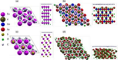
Figure 1. Side view and top view of the calculated crystalline structures for graphene on top of (a) EuO, (b) CoFe2O4, (c) EuS and (d) Y3Fe5O12 films. All the substrates used in the calculations are passivated with hydrogen atoms on the other surface.
Download figure:
Standard image High-resolution imageNext, we consider the lattice mismatch between graphene and YIG. Their lattice parameters are 2.46  and about 12.49
  , respectively. As shown in figure 1(d), the
  unit cell of YIG (1 1 1) substrate with a lattice constant of about 17.66
  can fit on the
  graphene unit cell, with a lattice mismatch of about 2.5%. The resulting supercell is composed of six YIG trilayers and a graphene layer placed on top. For CFO the bulk lattice parameter is 8.46
  and a
and a  graphene unit cell can fit on a
  CFO(1 1 1) substrate with a lattice mismatch of about 3.6%. The supercell in this case is composed of six trilayers of CFO with graphene on top of Fe atoms (see figure 1(b)). In all the cases, the bottom surface is passivated with hydrogen atoms in order to avoid the bottom surface effect on graphene and the vacuum region is chosen to be larger than 14
  . The lattice structure of graphene/MIs are presented in figure 1 with a vertical distance between Eu and C layers around 2.57
  and 2.52
  for EuO and EuS, respectively. For graphene/YIG and graphene/CFO, due to the large lattice mismatch, the graphene lattice is corrugated with corrugation heights of 0.6
  and 0.15
  for YIG and CFO, respectively. The average vertical distance between Fe and C atoms is close to 2.7
  for both YIG/graphene and CFO/graphene. This strong corrugation in graphene may affect its electronic band structure as shown previously for graphene on top of MgO substrate [54].
Finally, using the SIESTA package and the optimized structures of graphene on MIs shown in figure 1, we calculate the electronic structure of the systems with LDA + U for the exchange correlation functional (see table 1). The self-consistent calculations are performed with an energy cutoff of 600 Ry and with a  K-point grid for EuO and EuS and
  for YIG. A linear combination of numerical atomic orbitals with a double-ζ polarized basis set is used for the small structures and and a single-ζ for the larger ones. For graphene on CFO, the electronic structure is calculated using GGA + U as implemented in VASP package with a
  K-point grid.
3. Results and discussion
3.1. Electronic structure of graphene in proximity of MIs
Graphene honeycomb structure comprises two equivalent carbon sublattices A and B with charge carriers described by massless Dirac excitations. Of particular importance for the physics of graphene are the two Dirac points K and  at the corners of the graphene Brillouin zone (BZ). In the vicinity of these two points, the electronic structure of graphene is characterized by a linear dispersion relation with a Dirac point separating the valence and conduction bands with a zero band gap as follows:

where q is the momentum measured relative to the Dirac point and vF represents the Fermi velocity which does not depend on the energy or momentum [3]. The gapless Dirac cones at K and  are protected by time-reversal and inversion symmetry. Since Dirac points are separated in the BZ, small perturbations cannot lift this valley degeneracy. Once graphene is in proximity of a substrate, A and B sublattices feel different chemical environment which leads to the inversion symmetry breaking between K and
  and gives rise to a band gap. This can be modeled by the following Hamiltonian describing the graphene's linear dispersion relation in proximity of magnetic insulator:
where σ and s are the Pauli matrices that act on sublattice and spin, respectively. The second term represents the exchange coupling induced by the magnetic moment of magnetic atoms, with  , where
  and
and  being the strength of exchange spin-splitting of the hole and electron, respectively. The third term results from the fact that graphene sublattices A and B are now feeling different potential which might result in a spin-dependent band gap opening at the Dirac point and
  is the averaged staggered sublattice potential. The fourth one is a spin dependent mass term with
 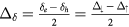 A Rashba spin orbit coupling term which might also occur at the magnetic insulator/graphene interface [36] and important for the anomalous quantum Hall effect (AQHE) and other spin orbit phenomena can also be added to the Hamiltonian and can be represented by
  at the left side of equation (2). This is beyond the scope of the current work and will be reported in future.
Let us now discuss the electronic band structures of graphene in proximity to MIs as shown in figure 2. For graphene on top of europium chalcogenides a  unit cell is used and due to the folding of graphene's BZ, both K and
  points get mapped to the
  point [35]. Therefore for EuO and EuS, the Dirac cone of graphene becomes located at the
  point instead of K ones. The linear dispersion of the graphene band structure is modified with a band gap opening at the Dirac point. Interestingly, this degeneracy lifting at the Dirac point is spin dependent as demonstrated for EuO [35]. The spin-dependent band gaps found in the EuO/graphene are about 134 and 98 meV for spin up and spin down states, respectively (see figure 2(a)). Here, however, we fit the band structure parameters according to Hamiltonian given by equation (2) to which the exchange splitting gaps of 84 and 48 meV are added for electrons and holes, respectively. Replacing EuO by EuS increases drastically the band gap opening as shown in figure 2(c). The spin-dependent band gaps in this case are about 192 (resp. 160 meV) for spin up (resp. spin down) states. However, the spin splitting is strongly reduced to 23 (resp. −10 meV) for electrons (resp. holes). This difference between EuO and EuS results from the fact that all 3 Eu atoms in EuS case are sitting in a hollow site of graphene hexagon while for EuO, the atoms belong to the bridge site and to the hollow site as shown in figures 1(a) and (c). Recently, Su et al [55] reported that while Eu atom sitting at the hollow site of graphene hexagon is described by an inter-valley scattering term in the induced proximity Hamiltonian, Eu atoms at the bridge site reduces the graphene lattice symmetry and can be represented by a valley pseudospin Zeeman term in x-direction in sublattice space that shifts slightly the Dirac cones from the
  point.
Figure 2. Band structures of graphene on (a) EuO, (b) CoFe2O4, (c) EuS and (d) Y3Fe5O12. Blue (green) and red (black) represent spin up and spin down bands of graphene (magnetic insulators), respectively. Graphene on EuO (1 1 1) case is taken from [35]
Download figure:
Standard image High-resolution imageLet us now discuss the proximity effects induced by yttrium garnet (YIG) and cobalt ferrite (CFO) oxides. In figure 2(d) we present the electronic bands of the YIG/Graphene structure where the proximity of YIG induces a band gap opening in graphene at the Dirac point. Furthermore, due to the interaction between graphene and the magnetic substrate, the spin-degeneracy around Dirac point is lifted. The spin-dependent band gaps found in the YIG/graphene are 116 and 52 meV for spin up and spin down states, respectively. The spin splittings estimated from the band structure are found to be about −52 and −115 meV for electrons and holes, respectively. Due to its interaction with the magnetic insulator, graphene becomes doped and the Dirac Cone is shifted below the Fermi level as seen in figure 2(d). Interestingly, the band structure presented in figure 2(d) shows that graphene on top of YIG has a half metallic behavior. The spin-up Dirac cone lies in the middle of the spin-down gap and vice versa. For the CFO/graphene case the induced band gap opening around the Dirac point is absent (see figure 2(b)). Nevertheless, due to the interaction between graphene and the magnetic substrate, the spin-degeneracy around Dirac point is lifted and spin-dependent band gaps are still induced in this case and found about 12 and 8 meV for spin up and spin down states, respectively. The strength of the exchange-splitting estimated from the band structure is −45 and −49 meV for electrons and holes, respectively. Graphene is slightly doped and the Dirac Cone is shifted above the Fermi level as seen in figure 2(b).
The extracted band gaps and exchange-splitting values at Dirac point induced in graphene by the proximity of magnetic insulators are summarized in table 2 with EG,  and
and  representing the energy band gap and the spin-dependent gaps for spin-up and spin-down, respectively. The spin splitting of the electron and hole bands are denoted as
  and
and  . Finally, ED indicates how large the Dirac point doping is with respect to Fermi energy. In table 2 the positive value of EG indicates a band gap between conduction and valence band, whereas negative value indicates a spin resolved band overlap as seen in CFO case shown in figure 2(b). Spin-splittings are defined by spin dependent energy differences at Dirac point with negative value indicating that spin-up bands are lower in energy than that of spin-down bands. The extracted values are compared with that aligned and misaligned EuO heterostructure with graphene between two EuO layers reported in [55]. As illustrated in table 2, doping graphene with EuO will push further the Dirac point below the Fermi level and makes impossible to harvest the graphene linear dispersion in practical electronic devices. To overcome the problem of strong doping one can deposit on the top side of the structure a material which can hole dope graphene. For instance, we propose that CFO deposited on the top side of europium chalcogenides/graphene or even YIG/graphene will bring Dirac cone closer to Fermi level and the exchange-splitting parameter induced by proximity effect, in such a heterostructure, is expected to be doubled in the range of hundreds of meV. Moreover, this type of asymmetric heterostructure will break the in-plane inversion symmetry of the graphene layer and might give rise to topological properties such as quantum anomalous Hall effect [55].
Table 2. Extracted energy gaps and exchange splitting parameters of graphene/MIs structures at Dirac point compared with parameters for graphene in proximity of EuO heterostructure reported in [55]. EG is the band-gap of the Dirac cone.  and
and  are the spin-up and spin-down gaps, respectively. The spin-splitting of the electron and hole bands at the Dirac cone are
  and
and  , respectively. ED is the Dirac cone position with respect to Fermi level.
| Structure | EG (meV) |  (meV) (meV) |
 (meV) (meV) |
 (meV) (meV) |
 (meV) (meV) |
ED (eV) |
|---|---|---|---|---|---|---|
| EuO/Gr/EuO(1BL) aligned [55] | 127 | 309 | 344 | 182 | 217 | −2.8 |
| EuO/Gr/EuO(1BL) misaligned [55] | −38 | 137 | 182 | 211 | 220 | −2.8 |
| Gr/EuO(6BL) | 50 | 134 | 98 | 84 | 48 | −1.37 |
| Gr/EuS(6BL) | 160 | 192 | 160 | 23 | −10 | −1.3 |
| Gr/Y3Fe5O12 | 1 | 116 | 52 | −52 | −115 | −0.78 |
| Gr/CoFe2O4 | −37 | 12 | 8 | −45 | −49 | +0.49 |
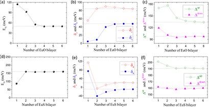
3.2. Thickness variation effect on the graphene exchange parameter in proximity of europium chalcogenides
Finally, let us check the robustness of aforementioned results by exploring the variation of the energy band gaps and proximity exchange-splitting in graphene at Dirac point as a function of MIs thicknesses. As seen in figure 3, all the plotted values tend to saturate above a thickness of 3 bilayers indicating that 3 or 4 bilayers of MIs are sufficient to mimic the bulk effect. The results also indicate that MIs as thin as 1 bilayer of europium chalcogenides can induce large proximity effect in graphene. For instance, the spin-splittings of the electron and hole bands at the Dirac cone in the case of one bilayer of EuS (EuO) are found about 120 and 80 meV (55 and 5 meV), respectively. As EuS (EuO) thickness increases, both spin-splitting values decrease (increase) to reach the bulk values shown in table 2. As for spin-dependent band gaps  and
and  , both decrease as a function of MI thickness with variation of spin-down and spin-up band gaps being less dramatic in the case of EuS compared to that for EuO. Since the induced magnetism in graphene due to proximity of europium chalcogenides arises mainly from graphene hybridization with polarized Eu-4f state right below the Fermi level [35], the observed variation at low thicknesses is related to the variation of the energy level of these Eu-4f states.
Figure 3. Thickness variation of the exchange-coupling parameters presented in table 2 for the graphene in proximity of chalcogenides EuO and EuS.
Download figure:
Standard image High-resolution image
4. Conclusion
In summary, using first-principles calculations we investigated proximity effects induced in graphene by magnetic insulators. Four different MIs have been considered: two ferromagnetic europium chalcogenides and two ferrimagnetic insulators yttrium iron garnet and cobalt ferrite. In all cases, we find that the exchange-splitting induced in graphene varies in the range of tens to hundreds meV. While Dirac cone is negatively doped for graphene on europium chalcogenides and YIG, it is found to be positively doped for graphene on CFO substrate. In order to bring the Dirac cone closer to the charge neutrality point, we propose to deposit on the top side of the negatively doped structure a material which can positively dope graphene, such as CFO. In such a heterostructure the exchange-coupling parameter induced by proximity effect is expected to be doubled. Moreover, we explored the variation of the extracted magnetic exchange parameters as a function of europium chalcogenides thicknesses. This analysis shows that the extracted parameters are robust to thickness variation and one monolayer of magnetic insulator can induce a large magnetic proximity effect on graphene. These findings pave the way towards possible engineering of graphene spin-gating by proximity effect especially in view of recent progress in experiments.
Acknowledgments
We thank Xavier Waintal for fruitful discussions. This project has received funding from the European Union's Horizon 2020 research and innovation programme under grant agreement No. 696656 (Graphene Flagship). SR acknowledges Funding from the Spanish Ministry of Economy and Competitiveness and the European Regional Development Fund (Project No. FIS2015-67767-P (MINECO/FEDER)), the Secretaria de Universidades e Investigación del Departamento de Economía y Conocimiento de la Generalidad de Cataluña, and the Severo Ochoa Program (MINECO, Grant No. SEV-2013-0295).