

Abstract
We report on a scanning confocal Raman spectroscopy study investigating the strain-uniformity and the overall strain and doping of high-quality chemical vapour deposited (CVD) graphene-based heterostuctures on a large number of different substrate materials, including hexagonal boron nitride (hBN), transition metal dichalcogenides, silicon, different oxides and nitrides, as well as polymers. By applying a hBN-assisted, contamination free, dry transfer process for CVD graphene, high-quality heterostructures with low doping densities and low strain variations are assembled. The Raman spectra of these pristine heterostructures are sensitive to substrate-induced doping and strain variations and are thus used to probe the suitability of the substrate material for potential high-quality graphene devices. We find that the flatness of the substrate material is a key figure for gaining, or preserving high-quality graphene.
Export citation and abstract BibTeX RIS
1. Introduction
For over a decade, graphene has been in the spotlight of solid state research. Its high charge carrier mobilities [1–4] and long spin diffusion lengths [5, 6], as well as its optical [7] and mechanical properties [8] promise a wide range of applications ranging from spintronics [9] to high frequency electronics [10], ultra-sensitive sensors [11, 12] and flexible optoelectronics [13]. In order to advance prototype devices to true applications, large effort has been put into growth [14–18] and contamination-free transfer [3, 4, 19, 20] of high quality graphene based on chemical vapour deposition. However, as graphene and other two-dimensional (2d) materials consist only of surface atoms, the choice of substrate material has a large influence on their structural and electronic properties [2, 21–25]. In this work, we investigate strain, doping and the strain uniformity of high quality CVD graphene/hBN heterostructures placed on different substrate materials. Here, we follow a recently reported, contamination free, dry transfer process, where exfoliated hBN is used to pick up CVD graphene directly from the growth substrate. The obtained stack is subsequently placed on different target substrates [4]. This fabrication process yields high quality heterostructures with little intrinsic overall doping and low nanometre-scale strain variations. As the graphene crystal is covered, i.e. protected by hBN on the top side, modifications in doping and strain are purely due to the substrate at the bottom side of graphene, making our approach suitable for benchmarking the substrate suitability.
2. Sample fabrication
We grow individual graphene crystals with a typical diameter of a few hundred micrometers using a low pressure chemical vapour deposition process at a growth temperature of 1035 °C on the inside of enclosures folded from commercial copper foil (AlfaAesar 46365). Growth is carried out in a hydrogen/methane atmosphere (45 sccm and 5 sccm respectively) at a total pressure of 0.1 mbar for two hours [14]. Similar to previous works, we let the interface between graphene and copper oxidise under ambient conditions for a few days prior to transfer, in order to weaken the adhesion of the graphene to the copper foil [3, 4]. Figure 1(a) shows an optical microscope image of an individual graphene crystal a few days after growth. The bright orange colour is caused by the copper oxide layer on the copper-to-graphene interface. In order to transfer the graphene from the copper foil onto a different substrate, we employ a contamination-free van-der-Waals dry-transfer process. For the transfer, a polymer stamp consisting of a polydimethylsiloxane (PDMS) cushion is covered with a polyvinylalcohol (PVA)/ polymethylmethacrylate (PMMA) stack with a flake of exfoliated hBN on top. The hBN flake is aligned with the graphene and brought into contact at a temperature of 125 °C and separated again from the copper foil. Subsequently, the graphene/hBN stack is placed on different target substrates and the polymers are dissolved in deionized-water, acetone and isopropanol.

Figure 1. (a) Optical image of a graphene crystal on copper foil a few days after growth. The orange colour is due to the oxidised interface between graphene and the subjacent copper. (b) Optical microscope image of a hBN/CVD-graphene/hBN heterostructure. The black rectangle marks the area that has been mapped using confocal Raman microscopy. The red dashed line marks the sandwiched area. (c) Schematic of a hBN/graphene/substrate structure. (d) Typical Raman spectrum of CVD graphene encapsulated between two flakes of hBN. (e) Raman map of the line width of the Raman 2D-peak,  of the area marked in panel (b).
Download figure:
Standard image High-resolution image3. Results and discussion
Figure 1(b) shows an optical microscope image of a graphene/hBN stack placed on another flake of hBN. In figure 1(c), we illustrate a schematic of such a hBN/graphene stack on an arbitrary substrate. In previous works, we reported on very little overall doping concentrations ( cm−2) and low temperature (T < 2 K) charge carrier mobilities in the range of millions of cm2 (Vs)−1 for similar hBN/graphene/hBN structures [3], indicating that the transfer process avoids degradations of the graphene quality [3, 4]. In order to investigate the quality of the resulting substrate/graphene/hBN stacks, we use scanning confocal Raman microscopy, which is a fast and non-invasive method for probing a number of material properties of graphene including strain, doping, defects and nanometre-scale strain variations [26–32]. Confocal Raman microscopy was carried out using a WiTec 300 system using a laser with 532 nm wavelength and a typical laser power of 1 mW. Regions with cracks and folds in the hBN are disregarded in the analysis. Figure 1(d) shows a typical Raman spectrum of graphene sandwiched between two flakes of hBN. The Raman peak originating from the hBN is located around
  cm−1. The absence of the Raman D-peak at 1345 cm−1 indicates a very low defect density in the transferred CVD graphene. The Raman G-peak located around
  cm−1 shows a full-width-at-half-maximum (FWHM),
  , of around 14.5 cm−1, indicating very little overall doping of the graphene-based heterostructure [33]. The Raman 2D-peak is located around
  cm−1. The FWHM of the 2D-peak,
  , is 17 cm−1 indicating a high sample quality [4]. Recently, it has been shown that the value of
  is related to the amount of nanometre-scale strain variations in the graphene lattice within the spot size of the laser [31]. This is particularly crucial as there are strong indications that nanometre-scale strain variations are a limiting factor for the charge carrier mobility in high-quality graphene [25]. This stresses the importance of using the line width of the Raman 2D-peak in order to characterise potential substrates for graphene. Figure 1(e) shows a Raman map of
  recorded in the area marked by the black box in figure 1(b). Here,
  is homogeneously distributed around 18 cm−1 over the entire sandwiched region of the sample (see red dashed line in figures 1(b) and (e)), indicating a homogeneous sample quality with little strain variations over the entire sandwiched area. Outside the sandwiched area where the hBN/graphene stack lays on SiO2,
  shows elevated values of around 23 cm−1, revealing substrate-induced strain variations in the graphene.
The data extracted from the collected Raman spectra on the CVD graphene/hBN sandwich area are very similar to those of high quality heterostructures obtained with exfoliated graphene [2, 24, 31], showing that neither the CVD growth nor our dry transfer method are limiting factors for the 'structural' quality (i.e. overall, 'microscopic' strain and nanometre-scale strain variations) and doping of the graphene-based heterostructures.
In order to investigate a method for identifying suitable other (potentially more scalable) substrate materials, we fabricate stacks of graphene/hBN heterostructures and place them on a number of different substrates. Figures 2(a)–(h) show optical images of graphene/hBN stacks on such different substrate materials. The substrates investigated in this study are exfoliated flakes of hBN, transition metal dichalcogenides (TMDCs) such as WSe2 and MoS2, Si++/SiO2, sapphire (with two different roughness values), SrTiO3, graphene/hBN suspended over trenches, silicon, hydrogen-terminated fused silica, aluminium nitride (AlN) and cross-linked SU-8 (negative epoxy resist from MicroChem). These substrates cover the material classes of oxides, nitrides, silicon, polymers and 2d-materials. With this selected set of substrate materials, we investigate in particular technologically relevant substrate materials as well as upcoming 2d materials, which have already been shown to be good and potentially scalable substrates for graphene [22]. In order to understand the influence of the surface roughness of the substrate on the structural properties of graphene, the substrate roughness is measured using atomic force microscopy (AFM). Figures 2(i)–(p) show AFM images of the different substrates used. The AFM maps are used to extract the root mean square (RMS) values of the surface roughness for the individual substrate materials. In general, the 2d-materials hBN, WSe2 and MoS2 show the smallest roughness with RMS values less than 0.2 nm. The silicon, sapphire and Si++ /SiO2 substrates have RMS values between 0.25 and 1 nm. The investigated, hydrogen-terminated fused silica, SrTiO3 and SU-8 have a roughness between 2 nm and 4 nm and the AlN substrate has the largest roughness with an RMS value of 26 nm. Kretinin and co-workers [22] report RMS values of 0.1 nm for hBN and TMDCs and around 1 nm for the oxides they investigated, which compares well with the values we observe. Independently, it is important to note that the measured RMS roughness values are not intrinsic substrate properties, but are generally influenced by the used deposition method and subsequent substrate treatments. Even though exfoliated 2d materials typically show a very low intrinsic roughness, we would like to point out that single crystalline oxidic substrates can have a comparable roughness. Moreover, we would like to emphasize that here we selected a rather wide spread of surface roughnesses for investigating its relation with the Raman 2D line width.
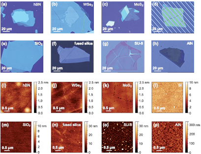
Figure 2. Optical microscope images of the hBN/graphene/substrate heterostructures based on different substrates including (a) hBN, (b) WSe2, (c) MoS2, (d) graphene hBN suspended over trenches, (e) Si++ /SiO2, (f) fused Silica (g) SU-8, and (h) aluminum nitride (AlN). Atomic force microscopy images of the substrate materials including (i) hBN, (j) WSe2, (k) MoS2, (l) Silicon, (m) Si++ /SiO2, (n) fused Silica (o) SU-8, and (p) aluminium nitride (AlN).
Download figure:
Standard image High-resolution imageIn figure 3, we summarize all the information about substrate-induced strain, doping and nanometre-scale strain variations obtained from the Raman maps of graphene/hBN on the selected substrate material by showing scatter plots of  and
and  . The amount of nanometre-scale strain variations is linked to
  , which is colour coded in the data points in each panel. In particular, we observe that graphene on hBN, WSe2, MoS2, and SiO2 shows low nanometre-scale strain variations as seen by the small values of
  (blue colour of data points), whereas substrates like SrTiO3, AlN and SU-8 show very large values of
  . Besides nanometre-scale strain variations, the overall doping (which also is connected to doping variations) strongly influences the transport properties of graphene. In order to compare the amount of substrate-induced strain and doping in graphene for the different substrates, we follow the method reported by Lee et al [32] and employ a 'vector' decomposition model on the position of the G-peak and the 2D-peak. A schematic of the influence of strain, doping and dielectric screening of the substrate is depicted in figure 3(l). Strain shifts the 2D-peak and G-peak positions with a relative slope of 2.2, which is related to the ratio of the Grüneisen parameters for the 2D-peak and the G-peak phonons [31, 32] (see black solid line in figure 3(l) and all other panels of figure 3). Hole doping shifts
  and
and  with a relative slope of 0.7 (black dashed line in figure 3(l) and all other panels of figure 3) and n-doping results in a non-linear decrease of
  [32, 34] (see black dotted line in figure 3(l)). The point of zero strain and zero doping is marked by the black circle. We applied a method by Berciaud et al [36] and Lee et al [32] in order to determine this point by measuring Raman spectra of pristine suspended graphene. The graphene was in this case directly exfoliated onto a Si/SiO2 chip with holes etched into the substrate (sample not shown). The G-peak and the 2D-peak of this pristine graphene sample are located at
  cm−1 and
  cm−1, respectively. In addition to strain and doping, dielectric screening of the substrate material has been shown to shift the peak positions of the G-peak and the 2D-peak as represented by the arrows in figure 3(l) [30]. A red shift of the G-peak for low n-doping can be neglected at room temperature, but should be taken into account at low temperatures [37].

Figure 3. (a)–(k) Scatter plots of  versus
  extracted from the spatially resolved Raman maps recorded on different substrates. Strain and doping of the graphene can be extracted using a kind of vector decomposition model [32]. The black dashed lines correspond to the doping axes and the black solid lines correspond to the strain axes. The black circles represent the point of pristine unstrained graphene. (l) Schematic representation of the influence of strain, p- and n-doping, as well as dielectric screening on
  and
and  .
.
Download figure:
Standard image High-resolution imageNow we have everything to read the information encoded in figures 3(a)–(k). We first compare how far the data points are shifted from the strain axis (black solid line). In particular offsets to the right indicate a minor electronic quality as they are caused by significant doping and doping variations leading to an increased Coulomb scattering. In contrast, small offsets to the left of the black solid line are caused by substrate-induced screening effects, not affecting the (electronic) quality of graphene. Moreover, pure shifts on the strain axis, i.e. the presence of homogeneous overall strain is considered to only very weakly influence the electronic properties of graphene. This at least holds for strain values below 1% [35]. All this allows to interpret our data, leading e.g. to the conclusion that WSe2 and MoS2 (only left shifts) are better substrates than SiO2 or sapphire (doping present), even though both substrate classes show almost the same amount of nanometre-scale strain variations. Furthermore, it becomes obvious that the rough SrTiO3, AlN and SU-8 which we investigated do not only introduce significant nanometre-scale strain variations, but also lead to substantial charge carrier doping in graphene, making these substrate materials not very suitable for high-quality graphene devices. Importantly, these observations can not be generalized to other substrates made out of these materials, as the surface roughness and interface termination crucially depend on the specific substrate preparation. Notably, the graphene suspended over trenches shows a slightly broadened distribution of  and
and  and elevated values for
  , which most likely results from an transfer related contaminations, degrading the graphene quality through the open trenches in the substrate.
Figure 4 shows the individual histograms of the  values extracted from Raman maps of graphene/hBN on all substrates investigated. The histograms for hBN and WSe2 and MoS2 show very low values of
  , indicating a very low amount of nanometre-scale strain variations, which makes these 2d materials suitable substrates for graphene. Interestingly, these materials exhibit a sharp lower cut-off at around 16 cm−1 suggesting this to be the intrinsic, non-broadened line width of the Raman 2D mode for our laser wavelength. In contrast, the rougher substrates such as SiO2, the rough sapphire and SrTiO3 show elevated values of
  . Both, AlN and SU-8 show extremely high values of
  of up to 50 cm−1 in combination with broad distributions suggesting not only a very high amount of nanometre-scale strain variations, but also non-homogeneous sample properties.

Figure 4. Histograms of  values extracted from the Raman maps taken on the graphene/hBN heterostructures placed on the different substrates investigated. The colour code is adapted from figure 3.
Download figure:
Standard image High-resolution imageIn figure 5, we plot the sample averaged  versus the RMS values of the surface roughness of the substrate material to explore how the presence of nanometre-scale strain variations is related to the surface roughness. The error bars plotted in figure 5 indicate the 20th and the 80th percentile of the corresponding distributions of
  . The hollow data points belong to the 2d materials, which exhibit a self cleaning effect [22]. Notably, we used in this graph data points from multiple sapphire and SiO2 samples, that have been prepared with different surface roughness, highlighting the importance of substrate preparation. The black dashed line is a guide to the eye, indicating an increase of the sample averaged
  value as function of an increasing RMS value of the surface roughness. This observation suggest that very flat substrate materials induce very little nanometre-scale strain variations in graphene and—as long as they do not induce large doping/doping variations—are well suited as substrate for high mobility graphene [25]. A similar relation between
  and the surface roughness has been observed for the case of graphene on metallic substrates [38]. However, in contrast to Zhao et al [38], we observe a smaller variation of
  as function of substrate roughness, which may result from the fact that the graphene/hBN heterostack is stiffer than a single layer of graphene and is thus less susceptible to strain than a single layer of graphene on a rough substrate.

Figure 5.  versus substrate roughness. The open data points mark the 2d-layered materials that show self cleaning properties. The black line is a guide to the eye, indicating an increasing
  for increasing surface roughness.
Download figure:
Standard image High-resolution image
Table 1 summarizes our findings including the specific RMS values of the surface roughness used for our exemplary substrate materials, the sample averaged values of the FWHM of the 2D peak,  and the mean values for the position of the G-peak
  and of the 2D-peak
  for all substrate materials investigated. For low doping concentrations, the absolute strain can be estimated from the G-peak and 2D-peak positions. However, precisely quantifying the exact doping level proves to be more difficult as the slopes for p-doping and n-doping are different [32] and dielectric screening has to be taken into account [30]. Finally, we compare the overall trend of surface roughness RMS and
  values with room temperature (RT) transport data from literature. The highest mobilities are known for hBN sandwich devices with values in the range of 75 000 to 100 000 cm2 (Vs)−1 [2, 4] followed by RT mobility values on the order of 15 000 cm2 (Vs)−1 for SiO2 [39] and mobilities of 10 000 cm2 (Vs)−1 at 50 K for flat SrTiO3 (roughness of 0.2 nm) [42] substrates. Lower carrier mobilities have been reported for fused silica (5000 cm2 (Vs)−1 [40]), sapphire (2000 cm2 (Vs)−1 [41]), AlN (1300 cm2 (Vs)−1 [43]) as well as SU-8 (1300 cm2 (Vs)−1 [12]). The overall trend of the RT carrier mobility when taking different roughness values into account is in reasonably good agreement with our observations (see data clouds in figure 5 and table 1). However, it is important to note that the detailed properties substantially depend on the substrate roughness and thus on the way how the substrates are prepared.
Table 1. Representation of the surface roughness (RMS), the sample averaged values of the FWHM of the 2D peak,  and the mean values for the position of the G-peak
  and of the 2D-peak
  for all substrate materials investigated. Using the vector decomposition model of Lee et al [32], we extract the average strain from the Raman maps.
| RMS (nm) |  (cm−1) (cm−1) |
 (cm−1) (cm−1) |
 (cm−1) (cm−1) |
Strain (%) | |
|---|---|---|---|---|---|
| hBN | 0.17 | 18.2 | 1583.8 | 2682.6 | −0.07 |
| WSe2 | 0.19 | 21.8 | 1587.2 | 2690.9 | −0.24 |
| MoS2 | 0.09 | 22.0 | 1585.1 | 2690.7 | −0.28 |
| SiO2 | 0.53 | 22.8 | 1585.5 | 2682.5 | −0.03 |
| SiO2 | 0.81 | 24.7 | 1590.9 | 2683.9 | 0.03 |
| Susp. | — | 24.5 | 1584.2 | 2682.3 | −0.05 |
| Fus. silica | 2.3 | 25.2 | 1585.6 | 2681.7 | −0.01 |
| Sapphire | 0.26 | 22.3 | 1585.1 | 2681.4 | −0.01 |
| Sapphire | 0.63 | 26.1 | 1587.1 | 2682.7 | −0.01 |
| Silicon | 1.0 | 26.9 | 1583.2 | 2685.9 | −0.17 |
| SrTiO3 | 2.8 | 28.8 | 1596.9 | 2683.4 | 0.17 |
| AlN | 26.2 | 30.0 | 1600.3 | 2681.7 | 0.28 |
| SU-8 | 3.7 | 33.6 | 1591.2 | 2681.0 | 0.12 |
4. Conclusion
In summary, we use spatially resolved confocal Raman spectroscopy as a fast, non-invasive characterization tool to investigate the suitability of different material classes as substrates for high quality of graphene, while excluding external or transfer related degradations by protecting the graphene with hBN on top. From the Raman spectra, we extract strain, doping and the strain uniformity for the different substrate materials and present the data in colour-coded scatter plots, which allows to easily decide whether a potential substrate material is suitable for high-quality graphene devices. The presented study suggests that 2d materials such as hBN, WSe2 and MoS2 are well suited substrates for graphene, as they possess low values of  and little overall doping. In contrast rougher substrates yield moderate values of
  and most oxidic substrates additionally introduce intermediate levels of charge carrier doping in graphene. These observations are in good agreement with typical results obtained from transport studies in these material systems [22]. In general, we observe a trend of decreasing strain uniformity with increasing substrate roughness.
5. Experimental details
The 2d materials used as substrates (hBN, MoS2, WSe2) have been exfoliated on Si/SiO2 substrates. The flakes have been chosen to be thicker than 20 nm in order to suppress the influence of the subjacent SiO2. The SiO2 substrate was thermally grown on a silicon wafer with an intrinsic roughness of 0.5 nm. To highlight the influence of the substrate roughness, the surface roughness of multiple SiO2 samples was increased using an CF4 plasma to RMS values of 0.8 nm. In addition, commercial wafers of crystalline fused silica, silicon, SrTiO3 and sapphire were used. Two sapphire substrates with different surface roughness were used. AlN has been deposited on Si substrates using atomic layer deposition (ALD). SU-8 was spin coated and onto a silicon substrate and baked. Fused silica and AlN have been annealed in an Ar/H2 atmosphere prior to transfer.
Acknowledgment
We thank C Neumann for helpful discussions and gratefully acknowledge support by the Helmholtz-Nanoelectronic-Facility (HNF), the DFG (SPP-1459), the ERC (GA-Nr. 280140), and the EU project Graphene Flagship (contract no. NECT-ICT-696656). Growth of hexagonal boron nitride crystals was supported by the Elemental Strategy Initiative conducted by the MEXT, Japan and JSPS KAKENHI Grant Numbers JP26248061, JP15K21722 and JP25106006.