
Abstract
Monoclinic group 6 transition metal dichalcogenides (TMDs) have been extensively studied for their intriguing 2D physics (e.g. spin Hall insulator) as well as for ohmic homojunction contacts in 2D device applications. A critical prerequisite for those applications is thickness control of the monoclinic 2D materials, which allows subtle engineering of the topological states or electronic bandgaps. Local thickness control enables the realization of clean homojunctions between different electronic states, and novel device operation in a single material. However, conventional fabrication processes, including chemical methods, typically produce non-homogeneous and relatively thick monoclinic TMDs, due to their distorted octahedral structures. Here, we report on a post-patterning technique using laser-irradiation to fabricate homojunctions between two different thickness areas in monoclinic MoTe2. A thickness-dependent electronic change from a metallic to semiconducting state, resulting in an electronic homojunction, was realized by the optical patterning of pristine MoTe2 flakes, and a pre-patterned device channel of monoclinic MoTe2 with a thickness-resolution of 5 nm. Our work provides insight on an optical post-process method for controlling thickness, as a promising approach for fabricating impurity-free 2D TMDs homojunction devices.
Export citation and abstract BibTeX RIS

Original content from this work may be used under the terms of the Creative Commons Attribution 3.0 licence. Any further distribution of this work must maintain attribution to the author(s) and the title of the work, journal citation and DOI.
Introduction
Transition metal dichalcogenides (TMDs) have received great attention beyond graphene because of their diverse structural and electronic properties [1–3], which are promising for applications in two-dimensional (2D) optoelectronic [4, 5], spintronic [6–8], and valleytronic devices [9–12]. Unlike graphite or hexagonal boron nitride (h-BN), the 2D layered TMDs show thickness-dependent electronic changes, especially in their atomically-thin geometry [13–15]. Direct-to-indirect bandgap transitions, semimetal-to-semiconductor transitions and inversion symmetry breaking phenomena have been demonstrated based on thickness control [15–17]. Along with unique strong spin–orbit coupling and low-dimensionality, such transitions are expected to derive synergetic applications for a future 2D-based industry [18–20].
Controlling the thickness of large-area 2D materials has been an important long-standing issue in the 2D community [21, 22]. For graphene and hexagonal TMDs, chemical vapor deposition (CVD) [23–25] and liquid exfoliation [26, 27] methods have been developed to address the issue. However, CVD and other chemical methods have limitations when it comes to producing thickness-controlled monoclinic TMDs (e.g. MoTe2) [28–30]; inevitable impurities and oxidation occur in the processes [31, 32]. This interferes with the fine thickness-control-based phase transition of monoclinic TMDs, which is essential for electronic and energy device applications of the materials. Moreover, recent studies have demonstrated that to control the phase transition of monoclinic TMDs, thickness control needs to be atomic-scale and widely homogeneous.
While a laser-thinning process has been developed for monolayer graphene and MoS2 [33, 34], these previous studies did not consider thickness-dependent electronic change or homojunctions. This optical technique has not yet been applied to monoclinic TMDs due to the absence of target single-crystalline materials and a lack of understanding regarding the thickness-dependent electronic change, as well as the thinning mechanism. It has been known that a local electronic change between semimetal and semiconductor can be achieved by a local thickness control of monoclinic TMDs [13, 35]. Moreover, the scalable optical technique (laser-thinning) can be extended to the semiconductor industry-level resolution (~10 nm) that has been also realized by optical lithography technique. However, it remains a challenging undertaking to realize homojunction devices with monoclinic TMDs based on the local thickness control.
Here, we report on a post-patterning technique using laser-irradiation to fabricate an atomically-thin homojunction device from monoclinic (known as a 1T' phase in other literatures) MoTe2. The term post-patterning means that the laser-irradiation is applied to pre-patterned device channels. This method enables a scalable design of electronic homojunctions based on thickness-dependent electronic change without any structural change, in contrast to the previous exfoliation-driven [13] and lattice-change-driven devices [39].
After fabricating a MoTe2 device, local laser-irradiation was used to decrease the thickness of the monoclinic MoTe2 channel down to 3 layers in desired areas, with vertical and lateral space resolutions of 5 nm and 500 nm, respectively; the vertical resolution of 5 nm indicates the resolution of thickness control and the 500 nm is originated from the optical resolution by a laser with a wavelength of 532 nm. We used the laser with a wavelength of 532 nm to verify the crystal structures via reliable Raman spectroscopy during post-patterning process. Therefore, the spatial resolution of our post-patterning is just limited by the long wave length that can be resolved in the future study. Raman and photoemission spectra of the laser-thinned monoclinic MoTe2 regions showed there were no structural changes or oxidation. By converting the thick metallic channel into a thin semiconducting channel, the trivial semimetal device was transformed into a semiconducting homojunction device. This study found that the laser-patterned thin flake region possessed physical properties similar to exfoliated few-layered single-crystalline monoclinic MoTe2. Therefore, we propose this method as a practical way to design homojunction devices with 2D materials.
Results and discussion
High quality single-crystalline monoclinic MoTe2 samples were synthesized as described in our previous reports [13]. Two different polymorphs of MoTe2, a semiconducting hexagonal and a metallic monoclinic MoTe2, were grown by a temperature quenching method, and the monoclinic MoTe2 single crystals were used in this study. The mechanical exfoliation, laser irradiation and friction force microscopy were conducted in air. The energy and power of the NTEGRA system (NT-MDT) laser were selected to be 532 nm (excitation wavelength) with 15 mW (power) for the laser thinning of the flakes and post-patterning of the device. Temperature-dependent transport of the fabricated device was investigated using a lakeshore probe station system (Model CRX-VF; cryogen-free micro-manipulated probe station) to compare the performance of the device before and after the post-patterning.
The crystal structure of the layered monoclinic MoTe2, which has a distorted octahedron structural unit, is shown in figure 1(a). Like other 2D materials, a weak van der Waals interaction exists between layers in the monoclinic MoTe2 crystals [36]. But lattice distortions, or atomically uneven layers, make exfoliation of the thin monoclinic MoTe2 more difficult compared to other flat 2D materials such as graphene and hexagonal TMDs [37].

Figure 1. (a) The crystal structure of monoclinic MoTe2 showing the structural unit, a distorted octahedral composed of Mo (blue-green) and Te (yellow) atoms. A top view and side view of the monoclinic MoTe2 are shown. (b) Schematic illustration of the laser-thinning process on monoclinic MoTe2. (c) Raman spectra before (black), during (red), and after (blue) the laser-thinning process. (d) Change in Raman peak positions before, during, and after thinning of the monoclinic MoTe2.
Download figure:
Standard image High-resolution imageFigure 1(b) shows a schematic image of the laser thinning process of a monoclinic MoTe2 flake on SiO2/Si substrate. When the top MoTe2 layer is exposed to a laser, local heat accumulates, and sublimation of the layer spreads from the top with a vertical thickness-control resolution of 5 nm. We interpret the vertical thickness resolution to be a function of the thermal conductivity of this material, and therefore layer-by-layer thickness control should be achievable by determining the optimal design of the thermal conductivity in the target 2D layered materials.
During laser-irradiation, the local temperature on the top layer was estimated to be around 400 °C, based on the amount of red-shift in the Raman Ag and Bg peaks (figure 1(c)) [38]. The high temperature heating was conducted in air, and the thickness of the flake gradually decreased and then saturated at 3 layers; at the saturated thickness, the local temperature on the surface cannot be maintained due to rapid heat dissipation into the SiO2/Si substrate [39].
Figure 1(c) shows Raman spectra of monoclinic MoTe2 and the temperature-driven Raman shift during the laser-thinning. The red shifted Raman active modes during laser-thinning are restored to their initial positions when the temperature decreases to room temperature [42, 43]. The IR active Bu peak at 194.5 cm−1 shows a blue shift, and a new peak appeared at 138.7 cm−1 after the laser-thinning. The two peaks can be assigned IR active modes Bu with an unusual behavior (blue shift), which could be explained by the role of Te defects [40] in Raman spectroscopy; similar phenomenon, defect-induced symmetry breaking to produce IR active modes, has been reported [41].
In order to address the oxidation issue and observe other chemical changes in the material that may be induced by the laser-thinning process, we investigated changes in the chemical states of Mo and Te atoms in the laser-thinned monoclinic MoTe2 areas using x-ray photoemission spectroscopy (XPS). Since the laser-thinning involves local thickness engineering, and we intended to conduct post-patterning in the monoclinic MoTe2, we used synchrotron radiation (hν = 700 eV) with a 200 nm-sized x-ray spot in our characterization of the laser-thinned area. The scanning image of Mo 3d photoelectrons is well-matched to the optical image of monoclinic MoTe2 flakes exfoliated on SiO2/Si substrate in figure 2(a). The pristine and laser-thinned MoTe2 flakes have Mo and Te atoms as majority components as seen in the wide scan (figure 2(b)). After the laser thinning process, Si 2p and O 1s photoelectrons from SiO2 substrate are appeared because the sample thickness is similar to the probing depth of photoelectrons (see figure S2 (stacks.iop.org/TDM/4/024004/mmedia)). To examine the surface chemistry, fine scans of Mo 3d and Te 3d photoelectrons were taken from laser-thinned area. In XPS of thin flake on insulating substrate, unavoidable charging effect shifts binding energies of the material. Therefore, instead of binding energy values, we used the binding energy difference between Mo 3d and Te 3d photoelectrons to investigate the surface chemistry before and after laser thinning process in monoclinic MoTe2. The binding energy differences of laser-thinned monoclinic MoTe2 flakes are almost similar to the binding energy differences of MoTe2 single crystals, indicating no surface degradation, deformation or oxidation [39].

Figure 2. Photoemission spectroscopy using synchrotron radiation (hν = 700 eV) of the laser-thinned monoclinic MoTe2 flake. (a) the scanning image with Mo 3d photoelectrons and the optical image of laser-exposed and unexposed monoclinic MoTe2 flakes. (b) Wide scan, (c) Mo 3d, and Te 3d electrons taken from different positions of pristine and laser-thinned flakes (the positions of #2 and #3 are taken from the flake in figure 2(a), the position of #1 is taken from the another flake in figure S1). The experimental spectrum (opened circles) are plotted with fitting curves (Green lines). The fitting parameters of a Gaussian width, spin–orbit splitting and asymmetry (α of Donic-Sunsic curve) are presented in table S1 in the supporting materials.
Download figure:
Standard image High-resolution imageThe process of controlling thickness by varying laser exposure time is demonstrated in figure 3. Figure 3(a) shows the large flake that was chosen, with a thickness of 21 nm. Laser patterning was conducted in a square shape with different exposure times, as shown in figure 3(b). Six square areas of 3 µm × 3 µm were fabricated with different laser exposure times, 5 s, 10 s, 20 s, 30 s, 40 s and 50 s for each step (the spot size was 200 nm), respectively. The height profiles in figure 3(c), measured by atomic force microscope (AFM), show that thinned regions in the MoTe2 flake were reduced to 10 nm, 5 nm and 2 nm by exposure times of 5 s, 30 s and 50 s, respectively and the surface roughness of laser-thinned area is estimated to around 1 nm (figure S4). However, the optical contrast in figure 3(b) does not show different levels in the laser-thinned areas unlike the AFM data. This can be explained by light scattering on the laser-treated surface where the roughness is increased by the laser-thinning. In our study, the reliable vertical thickness control was about 5 nm (~7 layers).

Figure 3. Optical images of a thick monoclinic MoTe2 flake (a) before and (b) after the laser-thinning process. (c) Line profile of laser-thinned areas, processed for different exposure times. (d) AFM topographic image of the laser-thinned areas in (b). The line profiles in (c) taken from white lines. (e) Friction force mapping of the same area in (d). Scale bar size is 20 µm.
Download figure:
Standard image High-resolution imageSurface morphology and friction force mapping of the laser-thinned MoTe2 flake were simultaneously obtained by AFM. This surface-sensitive technique provides information on the atomic height and electronic structure of the engineered area; if an oxidized or insulating area appears after laser-thinning, a local friction force will be measured by the AFM and reveal the material change. Figures 3(d) and (e) show that the patterned areas and their surrounding areas have similar roughness and friction force. A subtle contrast in figure 3(e) can be explained by the increase of roughness in patterned areas during the laser-thinning. But, the overall consistent friction force in figure 3(e) indicates that there were no oxidized or insulating areas near the patterned areas, confirming again the XPS results presented in figure 2.
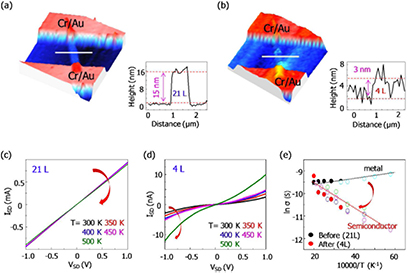
For an electronic homojunction device by the post-patterning, we applied the laser-thinning process to the device channel of a two-terminal monoclinic MoTe2 device that had been fabricated by a conventional exfoliation method. The average thickness of the channel following exfoliation was 15 nm (21 layers) with a lateral dimension of 5 µm as shown in figure 4(a). An AFM image of the post-patterned device (using the same device shown in figure 4(a)) is presented in figure 4(b). The thickness of the MoTe2 channel was decreased to 3 nm (4 layers) by the laser thinning, as shown in the line profile in figure 4(b). We note that it was difficult to obtain a few-layered monoclinic MoTe2 in which an electronic bandgap is opened by strong spin–orbit coupling, simply by this exfoliation [27]; this could be understood to be a consequence of the strong layer- to-layer interaction in monoclinic MoTe2, compared to graphite.
Figure 4. AFM topographic images of a monoclinic MoTe2 device (a) before and (b) after the post-patterning (laser-thinning) process. The thickness change of the device channel is described in the line profile. Temperature-dependent current-voltage curves of the device (c) before and (d) after the post-patterning process. (e) Arrhenius plots of device in (a) and (b) showing the appearance of a Schottky barrier in the post-patterned device.
Download figure:
Standard image High-resolution image
The post-patterning process in figure 4 allowed the channel to have semiconducting regions where atomically clean and thin homojunction could be generated. To demonstrate the electric characteristics of the post-patterned homojunction area, the temperature-dependent electric properties of the device were investigated before and after the laser thinning process, and the results are shown in figures 4(c) and (d). The thick channel device in figure 4(a), composed of 21 layers of monoclinic MoTe2, exhibits linear current–voltage curves (figure 4(c)), which proves the presence of a semimetallic channel and ohmic contacts in the device. In contrast, the post-patterned device with a 3 nm-thick channel in figure 4(b) exhibits non-linear current-voltage curves with largely increased resistance and semiconducting features; the resistance decreases as the temperature increases. Although the electric properties were completely changed by the post-patterning process, the thinned channel still showed the same Raman features described in figure 1(c), which indicates that monoclinic MoTe2 is robust to the laser-irradiation process. We further studied the device performance of laser-thinned semiconducting 1T' channel. Unfortunately, above the room temperature, the post-patterned devices exhibit almost zero ON/OFF ratio under the gating bias varying from −60 V to 60 V (see figure S5 in the supporting materials). This could be understood by large carrier density (~1014 cm−2) [13] and small bandgap (~60 meV) of 1T'-MoTe2 unlike other semiconducting TMDs which exhibit high ON/OFF ratio mostly due to their low carrier density (~1012 cm−2) and relatively large bandgap (~1 eV).
The thickness-driven electronic change from metallic to semiconducting states is clearly evidenced by the change in Schottky barrier heights of the two devices, which were fabricated using post-patterning on a single device, as shown in figures 4(a) and (b). In the Arrhenius plot of the conductance change as a function of temperature, the few-layered monoclinic MoTe2 device (red spots) shows a negative slope with an activation energy of ~60 meV, while the initial device (black spots) exhibits metallic characteristics. In order to more precisely compare the activation energy of our laser-thinned device with the activation energy of thin exfoliated flakes, we added three sets of transport data from thin exfoliated MoTe2 flakes (green, magenta and blue circles in figure 4(e)). The Schottky barrier height is consistent with the value obtained from the exfoliated thin monoclinic MoTe2 device (open circles), which demonstrates that our laser-thinning method produces a semiconducting MoTe2 characteristic that has been realized in high quality thin monoclinic MoTe2.
Recently, it has been reported that the thinner TMDs can have higher degree of disorder that causes a semiconducting transport behavior [44]. In our study, therefore, the exact physical origin of the semiconducting characteristics in thin 1T'-MoTe2 remains an open question: either bandgap opening owing to spin–orbit coupling like clean 1T'-MoTe2 single crystal or increased disorder effect in thin layer limit.
Conclusion
We demonstrated a laser-thinning method and its use in the post-patterning of an electronic homojunction in monoclinic MoTe2. A thickness-dependent electronic change from metallic to semiconducting states in the monoclinic MoTe2 was enabled by the fabrication of a homojunction between the thick metallic and thin semiconducting regions produced by the laser-thinning process. Despite of the unsatisfactory device performance of the laser-thinned MoTe2 compared to current transistor, we demonstrated that quantum physics, a new type of metal-insulator transition, can be linked to device application via the homojunction, a conceptually new device structure by our laser-thinning technique.
Investigation of the chemical states of Mo and Te atoms, and friction force, confirmed that the monoclinic MoTe2 is robust against the laser-irradiation process; oxidation and other degradation were negligible. The Raman spectra obtained during the laser-thinning process showed that the process of thermal detachment induced by the laser-irradiation effectively decreases the thickness of the monoclinic MoTe2 via local heating effect, at an estimated temperature of 300–400 °C. Vertical thinning and thickness were controlled to a resolution of about 5 nm, and the thinnest sample obtained with this method was 3 layers; realizing layer-by-layer thickness control with this method remains a challenge.
Considering that atomically-thin monoclinic MoTe2 or other group 6 TMDs have been difficult to obtain by chemical methods or mechanical exfoliation, our study suggests a breakthrough solution of this issue. Our thinned or post-patterned monoclinic MoTe2 shows physical characteristics that are similar to atomically thin monoclinic MoTe2. The post- phase-patterning is a practical way to realize few- layered monoclinic MoTe2 with a 500 nm lateral resolution for device applications, as well as for exploring novel physics such as 2D topological insulator.
Methods
Sample preparations
For the laser-thinning process, monoclinic MoTe2 flakes were mechanically exfoliated on SiO2 substrate using a conventional scotch tape method. The laser irradiation thinning process was performed with a laser power of 15 mW, while the Raman spectra were obtained with a laser power of 2.6 mW, which does not modify the sample.
Temperature estimation
Figure 1(c) shows Raman spectra taken before, during and after the laser-thinning process of the monoclinic MoTe2 flake. Because of the heating effect, the main peaks at 112.4 cm−1 (Ag), 128.9 cm−1 (Ag), 165.1 cm−1 (Bg), 194.5 cm−1 (Bu), 261.3 cm−1 (Ag) are red-shifted by ~4 cm−1. This indicates that the temperature increase of the sample surface is roughly 300–400 °C [39].
Friction force microscopy (FFM)
All AFM/FFM images were taken in E-sweep system with NanoNavi Station (Seiko) under ambient condition. The friction force was measured by the torsional displacement of the cantilever. In monoclinic MoTe2, the friction value was 10 mV smaller than the friction value of SiO2 substrate. The topography and friction mapping were obtained using Pt-coated tip with a spring constant of 0.2 N m−1 and a typical resonant frequency of 13 KHz. The FFM was conducted by a force set-point of 1 nN with a scanning speed of 30 µm s−1.
Scanning photoemission spectroscopy (SPEM)
SPEM measurements were performed at 8A1 beamline of the Pohang Accelerator Laboratory in Korea. The photon source was provided by a U 6.8 undulator, and the photon energy was set to 700 eV (photon energy resolution ~100 meV). The incident x-ray can be focused down to 200 nm using the Fresnel zone. The incident x-ray is perpendicular to the sample surface, and an electron analyzer (PHI 3057) is positioned at a fixed angle 54° from the incident direction.
Acknowledgments
This work was supported by Samsung Research Funding Center for Future Technology under Project Number SRFC-MA1502-09.