

Abstract
Large-area growth of monolayer films of the transition metal dichalcogenides is of the utmost importance in this rapidly advancing research area. The mechanical exfoliation method offers high quality monolayer material but it is a problematic approach when applied to materials that are not air stable. One important example is 1T'-WTe2, which in multilayer form is reported to possess a large non saturating magnetoresistance, pressure induced superconductivity, and a weak antilocalization effect, but electrical data for the monolayer is yet to be reported due to its rapid degradation in air. Here we report a reliable and reproducible large-area growth process for obtaining many monolayer 1T'-WTe2 flakes. We confirmed the composition and structure of monolayer 1T'-WTe2 flakes using x-ray photoelectron spectroscopy, energy-dispersive x-ray spectroscopy, atomic force microscopy, Raman spectroscopy and aberration corrected transmission electron microscopy. We studied the time dependent degradation of monolayer 1T'-WTe2 under ambient conditions, and we used first-principles calculations to identify reaction with oxygen as the degradation mechanism. Finally we investigated the electrical properties of monolayer 1T'-WTe2 and found metallic conduction at low temperature along with a weak antilocalization effect that is evidence for strong spin–orbit coupling.
Export citation and abstract BibTeX RIS
1. Introduction
In the surge of research into the properties of two-dimensional materials 'beyond graphene', transition metal dichalcogenides (TMDs) have emerged as a platform for novel scientific discoveries and exploratory device concepts [1–5]. TMDs, also known as MX2 materials, in the monolayer form consist of a layer of metal atoms, such as molybdenum or tungsten, sandwiched between chalcogenide atoms, such as sulfur or selenium. The optical [6], electrical [7], mechanical [8] and tribological [9] properties of these MX2 materials have been widely studied in recent years, with numerous proposed applications [10] including energy storage [11] and chemical sensors [12]. The majority of work to date has relied on mechanical micro-exfoliation to isolate flakes of high quality monolayer material but the yield for this method is typically very low, which makes comprehensive studies of monolayer MX2 films difficult and tedious. Therefore there is an urgent need for the development of robust and reproducible methods to produce high quality, large-area monolayer MX2 materials.
Monolayer MX2 films can be found in different structural phases [13], which differ in the arrangement of the top layer of chalcogenide atoms with respect to the bottom layer (figure 1(a)). MX2 materials frequently grow in the highly symmetric 1H phase where the top layer of chalcogenide atoms is aligned with the bottom layer. 1H-MoS2, the most commonly studied 1H material to this point, is a semiconductor which can be incorporated into field effect transistor (FET) devices with high on/off ratio, reasonable values of carrier mobility, and a band gap that is tuned by the number of atomic layers [14, 15]. In the 1T phase, the top layer of chalcogenide atoms is shifted with respect to the bottom layer so that as viewed normal to the plane, the chalcogenide atoms form a hexagon around the metal atom. The 1T phase of MoS2 has been accessed experimentally through chemical transformation induced by n-butylithium [16–18]. While 1H-MoS2 is a semiconductor, 1T-MoS2 is metallic, so lateral heterostructures of monolayer 1H/1T MoS2 are attractive candidates for developing low contact resistance devices [17]. The 1T' phase is a distorted 1T phase where the chalcogenide atoms have distanced themselves from their hexagonal position around the metal atom. The 1T' phase can be easily recognized and differentiated from the 1T phase by the presence of isolated zigzag chains of chalcogenide atoms that run vertically in figure 1(a).
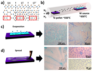
Figure 1. 1T'-WTe2 growth. (a) Ball and stick diagrams for the 1H, 1T and 1T' phases of WTe2. (b) Schematic of the growth process. (c) Optical micrograph of 1T'-WTe2 flakes grown by the evaporation method. Monolayer 1T'-WTe2 material appears as light gray 'webs' on the growth substrate. Darker multilayer regions are also observed. (d) Optical micrograph of 1T'-WTe2 flakes grown by the spread method.
Download figure:
Standard image High-resolution imageThe 1T' phase of TMDs has recently attracted great attention due to the prediction that they support topological electronic states [19]. For most of the MX2 materials, it has been predicted that the 1H phase is the energetic ground state, and that transitions from the 1H to the 1T' phase can be induced by strain [20]. One exception is WTe2, where the 1T' phase is predicted to be the ground state. Bulk crystals of 1T'-MoTe2 and 1T'-WTe2 have been grown, and exfoliation has been used to produce few-layer films, but monolayer films are rarely reported using this approach [21–23]. There are reports of a large non-saturating magnetoresistance [24], the appearance of weak antilocalization [23], and pressure induced superconductivity [25] in few-layer 1T'-WTe2, which is relatively stable under ambient conditions for films of six or more layers. However, since it is difficult to obtain monolayer flakes with reproducible properties by exfoliation, and because both 1T'-MoTe2 and 1T'-WTe2 are highly unstable under ambient conditions, there are to date very few studies of the properties of monolayer flakes. Recently we reported growth of monolayer single-crystal flakes of 1T'-MoTe2 by chemical vapour deposition (CVD) with good surface coverage, which enabled an extensive study of 1T'-MoTe2 in the monolayer form [26]. This was followed with a study on the absorption dichroism in monolayer 1T'-MoTe2 [27]. Recently a group has shown that growth of 1T'-WTe2 in monolayer form is possible by CVD [28] but there remains a need for careful investigation of the properties of monolayer flakes as well as a deeper understanding of the process of degradation under ambient conditions.
Here we present a facile, reproducible approach for growth of large, monolayer single crystal 1T'-WTe2 flakes by CVD with a surface coverage of ~20%. Monolayer 1T'-WTe2 flakes degrade within minutes under ambient conditions, but we found that by minimizing the handling time and passivating the samples with CVD-grown graphene, we were able to characterize monolayer flakes of 1T'-WTe2. The chemical composition of the films was determined using x-ray photoelectron spectroscopy (XPS), and atomic force microscopy (AFM) was used to confirm that the flakes were of monolayer height. Raman mapping was used to study the vibrational modes of monolayer and bilayer 1T'-WTe2, with the results being in excellent agreement with theoretically predicted phonon frequencies. Aberration corrected scanning transmission electron microscopy (ACSTEM) was used to determine that the WTe2 films were in the 1T' structural phase. Because the growth method produces a high density of monolayer 1T'-WTe2 flakes compared to the exfoliation method, we were able to study the degradation of the material in air. We explored degradation mechanisms by using density functional theory calculations and concluded that the films oxidize quickly in ambient. We obtained the first electrical results on monolayer 1T'-WTe2, finding a weak antilocalization effect at low temperature, which is consistent with the presence of strong spin–orbit coupling. This work creates a pathway towards the use of 1T'-WTe2 for integrated device structures whose operation relies on control of topological states and phases.
2. Growth process
The CVD process for monolayer 1T'-WTe2 flakes relies on deposition of W-feedstock material and a growth promoter [26] onto the growth substrate, followed by exposure to tellurium metal vapour at a temperature of 650 °C (a furnace schematic is shown in figure 1(b)). We developed two different methods for achieving monolayer 1T'-WTe2 flakes on a Si/SiO2 substrate, which differ only in the method used to apply the W source material (figures 1(c) and (d)). The first approach used a 5 nm thermal evaporation of WO3 (figure 1(c)), while in the second a large droplet of ammonia metatungstate was spread over a large fraction of the substrate (figure 1(d)). The second process was the most efficient, enabling dense growth of large (~50 µm) monolayer single crystal and polycrystalline 1T'-WTe2 flakes across a 2 cm × 3 cm Si/SiO2 substrate (figure 1(d)). Additional details are provided in the Methods section. Monolayer flakes grown by both methods showed identical physical and chemical properties. In the higher magnification optical images of figure 1(d), the top image shows regions of larger polycrystalline flakes that grew close to the initial source material, while monolayer single crystal flakes are seen further away from the initial ammonia metatungstate source. This suggests that the growth mechanism is similar to those for other TMDs such as 1T'-MoTe2 [26] and 1H-MoS2 [29, 30] where the ratio of Mo atoms to Te/S atoms is suitable for growth of monolayer single crystal flakes further from the Mo source.
3. Characterization of monolayer 1T'-WTe2 flakes
XPS and energy dispersive x-ray spectroscopy (EDS) were used to determine the elemental and bond composition of the 1T'-WTe2 flakes. Peaks in the x-ray photoelectron spectrum were observed at 573.0, 583.4, 243.7, 256.3 eV, corresponding to the Te 3d5/2, Te 3d3/2, W 4d5/2, and W 4d3/2 signals, respectively (figure 2(a)). These results are comparable to previous reports of XPS on exfoliated flakes of 1T'-WTe2 [22]. On the basis of these data, the Te/W atomic ratio was found to be 2.04, very close to the expected value for 1T'-WTe2. The full XPS spectrum and details as to how the stoichiometry was determined can be found in the supporting information and figure S1 (stacks.iop.org/TDM/4/021008/mmedia). The EDS results can be found in figure S2; they indicate a stoichiometry of 1:2, in good agreement with the XPS analysis. Atomic force microscopy (AFM) was performed on the flakes, revealing a height of roughly 1 nm (figure 2(b)) as expected for monolayers, and in agreement with previous reports on exfoliated 1T'-WTe2 flakes [21, 31]. Flakes grown through this method are predominantly monolayer thickness, but occasionally small bilayer regions are found on the edges of the flakes as seen in figures 2(b) and (c).
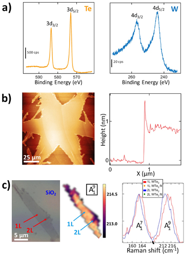
Figure 2. 1T'-WTe2 characterization. (a) XPS spectrum showing binding energies characteristic of 3d3/2 and 3d5/2 electron orbitals for Te, and the 4d3/2 and 4d5/2 orbitals for W. (b) AFM image of a large 1T'-WTe2 monolayer flake. AFM line scan shows that the flake height is ~0.8 nm, as expected for monolayer material. (c) (left) Optical image of a 1T'-WTe2 flake containing both monolayer and bilayer regions. (middle) Raman mapping of the  peak position of 1T'-WTe2 flake showing the difference in peak position between monolayer and bilayer. (right) The Raman spectrum shows that the
  peak for bilayer 1T'-WTe2 is close to to that for the monolayer, while the
  peak is shifted by ~1.5 cm−1.
Download figure:
Standard image High-resolution imageRaman mapping was performed on a 1T'-WTe2 flake that was predominantly monolayer but with small bilayer regions on the edges (figure 2(c)) in order to study the effect of this thickness change on the phonon modes. The flake was encapsulated with large-area graphene to avoid degradation during the measurements. Two main Raman peaks were observed: the in-plane  peak, and the
  peak, which contains both in-plane and out-of-plane vibrations [21]. For the monolayer region, the
  and
and  peaks were observed at 163.2 cm−1 and 214.7 cm−1, respectively. For the bilayer region the
  peak was at 162.7 cm−1, while the
  was shifted to 213.2 cm−1 (figure 2(c)). All of these peak positions are red-shifted by ~1 cm−1 compared to previously reported values [21, 23, 31, 32], but the separation between the
  and
and  peaks is in good agreement with these earlier works. To explain this observation, we used density functional theory to compute the frequencies of the Raman-active phonon modes before and after introduction of a graphene capping layer. For uncapped monolayer 1T'-WTe2 we calculate the position of the
  and
and  peaks at 161.54 cm−1 and 211.36 cm−1 respectively. With the addition of graphene, the peaks show a small red shift to 159.95 cm−1 and 208.35 cm−1. These calculated values are in good agreement with the measurements, and the calculation also explains the slight red shift in our data compared to earlier reports, which we attribute to the presence of the graphene capping layer. Using the same approach, we also studied the evolution of the Raman-active phonon modes as a function of layer number. We find that the
  should redshift from 211.36 cm−1 for monolayer material to 209.53 cm−1 for bulk, in agreement with our measurements and previous DFT studies [21, 31].
Monolayer and few-layer 1T'-WTe2 flakes are unstable under atmosphere as well as transmission electron microscopy (TEM) irradiation, so the 1T'-WTe2 flakes were encapsulated between graphene monolayers (figure 3(a)) to reduce damage during transfer and TEM imaging [33, 34]. (Details regarding the fabrication of the heterostructure stack can be found in the method section.) The intensity in high-angle annular dark field (HAADF) images is proportional to the square of the atomic number (Z) so the two graphene (ZC = 6) layers surrounding the 1T'-WTe2 monolayer (ZW = 74, ZTe = 52) are effectively invisible, making this graphene/MX2/graphene structure ideal for further studies on unstable materials. To determine the lattice parameters and image the atomic structure of monolayer 1T'-WTe2, selected-area electron diffraction (SAED) images and HAADF images were obtained using a JEOL 200CF (figure 3(c)) equipped with a CEOS corrector for the ACSTEM probe. The ACSTEM was operated at 60 kV to reduce beam-induced displacements of atoms from the lattice, although damage was observed at high magnifications after as little as one exposure. The symmetry of the graphene lattice is different from that of 1T'-WTe2, so the two diffraction patterns are readily distinguished. Figure 3(b) is the SAED image of the graphene/1T'-WTe2/graphene heterostructure, where the graphene diffraction spots are highlighted in blue and the 1T'-WTe2 spots in pink. The SAED pattern for 1T'-WTe2 matches the simulated SAED pattern in figure S3. Calibrating the SAED pattern using the graphene diffraction spots (![${{\bar{a}}_{\left[1\,0\,\bar{1}\,0\right]}}=\frac{\sqrt{3}\times 2.46\,{\mathring{\rm A}}}{2}=4.692$](https://content.cld.iop.org/journals/2053-1583/4/2/021008/revision1/tdmaa5921ieqn015.gif) nm−1) [35], we measure the lattice constants for 1T'-WTe2 to be a = 3.49 Å and b = 6.32 Å, in excellent agreement with previous reports [36]. The single crystal domain size is measured to be on the order of 10–20 µm2. Figure 3(c) is an HAADF image of the monolayer 1T'-WTe2 that shows excellent agreement with the simulated HAADF image in figure 3(d).
nm−1) [35], we measure the lattice constants for 1T'-WTe2 to be a = 3.49 Å and b = 6.32 Å, in excellent agreement with previous reports [36]. The single crystal domain size is measured to be on the order of 10–20 µm2. Figure 3(c) is an HAADF image of the monolayer 1T'-WTe2 that shows excellent agreement with the simulated HAADF image in figure 3(d).

Figure 3. TEM characterization of 1T'-WTe2. (a) Ball and stick model of the graphene-WTe2-graphene stack used for TEM imaging. (b) Inverted SAED pattern of the graphene-WTe2-graphene stack at 60 kV accelerating voltage. False colour has been added to distinguish between the 1T'-WTe2 (pink) and graphene (blue) diffraction spots. (c) High angle annular dark field (HAADF) image of monolayer 1T'-WTe2 at 60 kV accelerating voltage. (d) Simulated HAADF image of monolayer 1T'-WTe2 using quantitative image simulation in transmission electron microscopy (QSTEM) [37] with lattice parameters a = 6.282 Å and b = 3.496 Å [36].
Download figure:
Standard image High-resolution image4. Degradation of monolayer 1T'-WTe2 under ambient conditions
Bi-layer 1T'-WTe2 is reported to be unstable under ambient conditions, as evidenced by a decay in the Raman signal intensity over the course of several hours [21]. If bi-layer samples decay in hours, one might expect that monolayer samples decay much more quickly. To date, however, careful study of the stability of monolayer 1T'-WTe2 flakes has been problematic due to their rapid degradation and the low yield of the exfoliation method. Due to the relatively high coverage of monolayer 1T'-WTe2 flakes that is characteristic of our CVD growth process, we were able to observe the decaying of the monolayer flake through multiple experimental approaches. We first studied degradation of the material through measurements of the image contrast in optical micrographs, defined as ![$\left[{{I}_{\text{FL}}}-{{I}_{\text{SUB}}}\right]/{{I}_{\text{SUB}}}$](https://content.cld.iop.org/journals/2053-1583/4/2/021008/revision1/tdmaa5921ieqn016.gif) , where
, where  and
and  are the image intensity of the flake and the background oxidized silicon substrate, respectively (figure 4(a)). A sample of monolayer flakes was removed from the growth furnace and immediately transported to an optical microscope where it was left under ambient conditions for 3d (figure 4(a)). The optical contrast of the flake against the substrate was observed to decrease rapidly over time, suggesting that the flake underwent a chemical reaction with room air. After 30 min the optical contrast saturated at a low level, implying that the chemical reaction terminated.

Figure 4. Degradation of 1T'-WTe2 in air. (a) Time dependence of the optical contrast of a 1T'-WTe2 flake ('FL') compared to the SiO2/Si substrate ('SUB'). Contrast is defined as ![$\left[{{I}_{\text{FL}}}-{{I}_{\text{SUB}}}\right]/{{I}_{\text{SUB}}}$](https://content.cld.iop.org/journals/2053-1583/4/2/021008/revision1/tdmaa5921ieqn019.gif) . Inset: Representative optical images of the decaying flake. (b) Plot showing the decrease over time of the amplitude of
. Inset: Representative optical images of the decaying flake. (b) Plot showing the decrease over time of the amplitude of  and
and  Raman peaks of monolayer 1T'-WTe2. Inset: Optical micrograph of the 1T'-WTe2 flake used for the Raman measurements. (c) Optical microscope image after graphene transfer shows that there is a clear difference in the optical contrast of flakes exposed to air (lower right portion of image) compared to flakes passivated by graphene.
Download figure:
Standard image High-resolution imageWe studied the amplitude of the  and
and  peaks in the Raman spectrum of uncapped monolayer 1T'-WTe2 flakes left exposed to air (figure 4(b)). We first performed a scan on an as-prepared monolayer 1T'-WTe2 flake, and each scan at later times was conducted on a new, unmeasured flake in order to avoid the confounding influence of damage to the material caused by exposure to the Raman laser. Through this approach, we were able to study how exposure to room air affects the
  and
and  Raman peaks of monolayer 1T'-WTe2. The peak amplitudes decreased in a nearly identical manner, with a strong (~50%) reduction within a few minutes, and the peaks essentially disappeared after 30 min, in rough agreement with the optical contrast data of figure 4(a). To our knowledge this is first reported study of the decay of monolayer 1T'-WTe2 flakes under ambient using Raman spectroscopy. The results clearly indicate that monolayer 1T'-WTe2 flakes decay within tens of minutes when left unprotected under ambient conditions.
We discovered that degradation of monolayer 1T'-WTe2 could be avoided by transferring a sheet of graphene onto the substrate immediately after growth. The graphene-capped samples were stable for days, which enabled Raman mapping measurements, as illustrated in figure 2(c). Figure 4(c) is an optical image taken 12 h after a sample of monolayer 1T'-WTe2 flakes was partially capped with graphene. The top zoomed-in image shows that for monolayer flakes under graphene, the optical contrast against the oxidized silicon substrate remained very strong and was comparable to that observed for flakes immediately after growth. The bottom image is a portion of the sample where uncapped monolayer flakes were exposed to air for several hours. These flakes showed very low optical contrast, which is typical of degraded material, in agreement with figure 4(a). The middle image is of the region near the boundary of the graphene sheet. Some flakes in this region were half exposed to air, and the optical contrast of exposed regions was very different from that where the material was covered by the graphene overlayer. This image highlights the degradation of 1T'-WTe2 flakes in air and the utility of graphene as a passivation layer. Based on these measurements, we hypothesized that the films were damaged by reacting with a component molecule of the air.
5. Investigation of instability using density functional theory calculations
We explored possible degradation mechanisms by using density functional theory calculations to study the adsorption of H2(g), O2(g), and H2O(g) on monolayer 1T'-WTe2 as the first is present during synthesis and the latter two are ubiquitous. Figure 5(a) shows two perspectives of the 1T'-WTe2 (0 0 1) surface. The thickness of the monolayer under vacuum is 4.22 Å. The Te atomic layer lies on top of the layer of W atoms, which can have one of two geometries: small and large W3 triangles. In an oxygenated environment, 1T'-WTe2 favors the dissociative adsorption of O2(g), with the equilibrium structure at 0 K shown in figure 5(b). The adsorption process in the figure is highly exothermic (ΔEads = −3.60 eV/O2) and the adsorption location shown is greatly favored over other locations. Therefore surface oxidation by O2(g) is expected under experimental conditions of ambient O2(g) pressure and temperature. When O2(g) dissociates, one O atom binds directly atop a W atom in the sublayer. The other O atom displaces Te from a small W3 site, thus forming a W3O subunit. This site is favored over the large W3 triangle for dissociative O2 adsorption because it provides three-fold coordination for one of the O atoms. The displaced Te atom rises slightly off the surface (figure 5(c)), increasing the thickness of the monolayer from 4.22 Å to 5.12 Å. Therefore, this calculation suggests that 1T'-WTe2 is highly susceptible to oxidation, which leads to structural degradation via displacement of Te. We find that oxygen chemisorption transfers intensity in the Raman T spectrum from the  and
and  peaks to new modes in the Raman spectrum associated with the vibration of W–O bonds. We calculated Raman frequencies of 322.82 cm−1, 389.19 cm−1 for in-plane oxygen vibrations, and a mode at 500.03 cm−1 with predominantly oxygen out-of-plane vibrations.
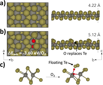
Figure 5. Surface structure of monolayer 1T'-WTe2(0 0 1). (a) Under vacuum. (b) In the presence O2. (c) Te displacement due to O2 molecules. The W, Te and O atoms are coloured grey, green and red respectively.
Download figure:
Standard image High-resolution imageWe also investigated the possibility that H2(g), present during synthesis, could passivate the surface. We find, however, that H2(g) prefers physisorption over dissociative chemisorption (figure S4(a)). This process is slightly exothermic with ΔEads = −0.07 eV/H2, and the thickness of the monolayer is unaffected by H2(g) adsorption. The surface greatly prefers oxidation to hydrogenation.
Finally, we considered the competition between O2(g) and H2O(g) as surface oxidizing agents (see supporting information). Unlike O2(g), H2O(g) prefers associative adsorption at Te sites. Figure S4(b) shows that H2O(g) weakly interacts with the surface by forming van der Waals bonds between H and Te, with no effect on the thickness of the monolayer. Adsorption is spontaneous (ΔEads = −0.27 eV/H2O) but the energetics are far less favorable than for dissociative O2(g) adsorption. Therefore, O2(g) is a much more potent surface oxidizer than H2O(g). Based on these considerations, we conclude that 1T'-WTe2 monolayer films degrade under ambient through oxidation, leading to the changes in optical contrast and the Raman spectrum that are discussed above.
6. Semimetallic nature of monolayer 1T'-WTe2
First-principles calculations were performed to confirm the semimetallic nature of monolayer 1T'-WTe2. As shown in figure S5, the Fermi level overlaps with the conduction and valance bands, forming electron and hole pockets near the Γ point. Nonetheless, since the bulk energy gap is well developed throughout the entire Brillouin zone, separating the conduction and valance bands, the time-reversal invariant Z2 topological phase [38] can be evaluated using the all the states from 1st to nth bands, where n is the electron filling. We find the Z2 topological invariant is nontrivial, as reported in a previous study [19]. The semimetallic nature of WTe2 obstructs disentanglement of the helical edge states of the nontrivial topological phase and the bulk metallic states. Nonetheless, the quantum spin Hall effect in WTe2 could potentially be observed by applying an external electric field or strain, which would induce a band gap and isolate the surface edges states from the bulk states [19].
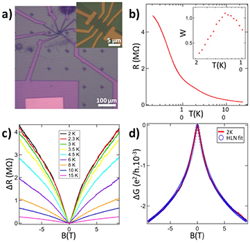
Devices for transport measurements on single monolayer flakes were fabricated by electron beam lithography with minimal material degradation due to air exposure. Details of the fabrication process are provided in the Methods section. Care was taken to define the contact pattern so that the electrical leads to a particular monolayer flake would not be short-circuited by other 1T'-WTe2 flakes on the substrate (figure 6(a)). The monolayer 1T'-WTe2 material was kept passivated by a PMMA layer, with only brief exposure to air. After fabrication, we carried out low temperature magnetoresistance measurements under high vacuum. Once the electrical measurements were completed, Raman spectroscopy was performed on the flake to confirm its monolayer thickness.
Figure 6. Electrical data of monolayer 1T'-WTe2. (a) Optical image showing the device structure with a visible window through the PMMA coating to the contact electrode. Inset: Optical micrograph of the monolayer 1T'-WTe2 flake device. (b) Resistance versus temperature behavior of the device. Inset: Reduced activation energy as a function of temperature showing metallic behavior. (c) Magnetoresistance for different temperatures, showing the appearance of the weak antilocalization cusp. (d) Magnetoconductance measurement at 2 K (red curve), fitted with Hikami–Larkin–Nagaoka (HLN) theory (blue circle). The results show excellent agreement between the data and the fit.
Download figure:
Standard image High-resolution image
We monitored the sample resistance in a 4-probe measurement configuration as the sample was slowly warmed from 2 K to 300 K (figure 6(b)). The insert of the figure shows the reduced activation energy  as a function of temperature revealing a positive slope at low temperature, indicating metallic behavior [39]. To our knowledge, these are the first measurements of monolayer 1T'-WTe2 showing this property. The sample magnetoresistance showed a cusp-like weak antilocalization (WAL) feature that became more pronounced and narrower at low temperature. The WAL effect can be associated with either bulk or topological states and its appearance here indicates that spin–orbit coupling is sufficiently strong that the spin orbit scattering length is much less than the phase scattering length [40–43]. WAL has been observed in multilayer 1T'-WTe2 [23] but until now has not been reported in monolayer devices, presumably because of their air sensitivity. The measured sample magnetoconductance was fitted with the Hikami–Larkin–Nagaoka (HLN) equation in the limit of strong spin orbit coupling,
 ![$\sigma (B)-\sigma (0)=-\alpha \frac{{{e}^{2}}}{\pi h}\left[\psi \left(\frac{1}{2}+\frac{{{B}_{\phi}}}{B}\right)-\ln \left(\frac{{{B}_{\phi}}}{B}\right)\right]\,$](https://content.cld.iop.org/journals/2053-1583/4/2/021008/revision1/tdmaa5921ieqn029.gif) [44], where ψ is the digamma function, and
[44], where ψ is the digamma function, and  with lϕ the phase coherence length (figure 6(d)). Agreement for all temperatures was excellent with the inferred phase coherence length ranging from 40 nm at 2 K to 22 nm at 15 K. The parameter α indicates the number of conduction channels, and is of order unity in topological insulators [23, 40, 41, 45–47]. In our measurements we found nearly 100% magnetoresistance at 2 K but HLN analysis yielded
  due to the high channel resistance (far exceeding the resistance quantum), indicating diffusive transport and no contribution from ballistic channels. We note, however, that we assumed conduction in the flake was uniform across its area when converting conductance into conductivity, and that the value of α would be systematically underrepresented if conduction actually occurred through a path significantly less wide than the flake width. Through these electrical results we conclude that monolayer 1T'-WTe2 possesses a strong spin orbit coupling effect, a first step toward realizing topological electronic states.
7. Conclusion
We have demonstrated a facile and reproducible growth method for achieving monolayer 1T'-WTe2 flakes. Samples were carefully characterized using XPS, Raman spectroscopy, AFM and ACSTEM to confirm their atomic composition and structural configuration. We demonstrated the use of a graphene overlayer to passivate the material and avoid degradation under ambient. Degradation occurs rapidly (minutes) and is most likely driven by a reaction with oxygen gas, as we demonstrated computationally. Finally we presented the first electrical data on monolayer 1T'-WTe2. A WAL effect appears at low temperature and is well fit by the HLN equation in the limit of strong spin orbit coupling. The approach presented here provides a pathway to further study of topological electronic states in this two-dimensional material.
7.1. Methods
7.1.1. CVD Growth of 1T'-WTe2
First a growth promoter of 2% sodium cholate in DI water was spin-coated onto the growth substrate at 4000 rpm for 60 s. Then several 100 µl droplets of a 3.1 mM solution of ammonia metatungstate were applied and spread gently across the chip using a brush with micrometer–diameter wires. The growth substrate was placed in the center of the CVD furnace, and a second chip containing 25 mg of tellurium was placed 5 cm upstream from the growth substrate (see figure 1(b) for a schematic of the growth system). The chamber was flushed for 5 min under a flow of 350 sccm of N2 and 22 sscm of H2, and then the furnace temperature was increased to 650 °C at a rate of 70 °C min−1. The growth substrate containing the W source material reached the furnace temperature of 650 °C, while the upstream tellurium material reached 550 °C and started to sublime. The furnace was held at 650 °C for a 6 min film growth period, and the furnace was then rapidly cooled under the same gas flows. The growth substrate was retrieved, and large amounts of monolayer 1T'-WTe2 flakes were found to have grown all across the substrate.
7.1.2. Device fabrication
To fabricate devices for transport measurements with minimal material degradation due to air exposure, samples were grown by CVD and then immediately spin-coated with 2 µm of C4 PMMA (Microchem) and inserted into the vacuum chamber of an electron beam lithography system. Markers in the PMMA were defined by electron beam lithography, and then optical microscopy was used to determine locations of single crystal monolayer 1T'-WTe2 flakes with respect to the markers. This map was then used to define electrical contacts to a single flake using electron beam lithography, which were then metallized with 5 nm of Cr and 25 nm of Au. Immediately after lift off the sample was again spin coated with C4 PMMA to minimize contact with air, and a second electron beam lithography step was used to open small windows on the electrode pads to enable electrical contact. This method ensured that the monolayer 1T'-WTe2 flake to be measured was kept passivated by a PMMA layer, with only brief exposure to air.
7.1.3. XPS
The chemistry of the near-surface region was investigated by XPS using a customized XPS spectrometer (VG Scienta AB, Uppsala, Sweden) [48]. XPS analyses were performed using a monochromatic Al Kα source (photon energy 1486.6 eV). The residual pressure in the analysis chamber was less than 1 × 10⁻⁸ Torr. The spectrometer was calibrated according to ISO 15472:2001 with an accuracy of ±0.05 eV. Survey and high-resolution spectra were acquired in constant-analyzer-energy mode with the pass energies of 200 and 100 eV, respectively. The spectra were processed using CasaXPS software (v.2.3.16, Casa Software Ltd., Wilmslow, Cheshire, U.K.). Background subtraction was performed using the Shirley–Sherwood method. Examples of XPS analysis performed with this spectrometer can be found in references [49, 50]. The quantitative evaluation of the XPS data was based on integrating the intensity of the W 4d5/2 and Te 3d5/2 peaks by taking the atomic sensitivity factors for those signals into account. The atomic sensitivity factors used were 2.6 for the Mo 3d5/2 peak and 5.4 for the Te 3d5/2 peak [40]. The reference energies for W 4d5/2 and the Te 3d5/2 peaks are 243.7 and 573.0 eV, respectively.
7.1.4. Graphene/MX2/graphene
Monolayer graphene was grown by CVD following the recipe discussed in the following paragraph. Two pieces of graphene were transferred by the bubble transfer method and left floating in deionized (DI) water. The first sheet of graphene was transferred onto a TEM grid and dried, while the second graphene sample was left in the water bath for later use. The PMMA layer used in the transfer process of the first graphene sheet was dissolved with acetone, followed by isopropanol (IPA). We then grew monolayer 1T'-WTe2 flakes by CVD, and once the growth was completed, the substrate was removed from the furnace and immediately covered with the second graphene sheet and dried. Through this method the 1T'-WTe2 experienced minimal exposure to air. The PMMA/graphene/1T'-WTe2 stack on the SiO2/Si growth substrate was then released using a diluted HF solution of 1:25 and quickly washed in 2 DI water baths before being transferred onto the first graphene sheet on the TEM grid. Acetone was then used to dissolve the PMMA followed by IPA. We were then left with a graphene/1T'-WTe2/graphene heterostructure on a TEM grid (figure 3(a)). The sample was stable in this configuration and could be transported to the ACSTEM for high resolution imaging.
7.1.5. Graphene growth
Graphene synthesis was carried out in a low-pressure CVD furnace (OTF-1200X-4-C4-SL-UL, MTI Corp.). Cu foils (Alfa Aesar Item #46365) were cleaned with 5.4% HNO3 for 40 s and two DI water baths for 2 min, and then blown dry with N2 gas. The reaction chamber was pumped to a base pressure of ~50 mTorr. The Cu growth substrate was annealed at 1020 °C for 30 min under a gas flow of 500 sccm Ar and 80 sccm H2. Monolayer graphene was then grown using methane as a carbon source at a flow rate of 5 sccm for 5 min and then 10 sccm for 15 min. The reactor was subsequently cooled to room temperature rapidly under a flow of 80 sccm H2 and 10 sccm CH4.
7.1.6. Structural stability calculations
Density functional theory calculations were carried out using the QUANTUM ESPRESSO code [51]. Designed, optimized, norm-conserving pseudopotentials [52] were used to soften the valence electron wavefunctions and ionic potentials of W and Te. Fully relativistic pseudopotentials were generated using the OPIUM code [53]. Pseudopotentials for H and O were generated with neutral reference electronic configurations. The reference electronic configurations of W and Te were 5s [2]5p [6]5d06s0 (W4+) and 5s [2]4d [10]5p [4] (Te2−) respectively. An augmentation operator was applied to the s potential of the W pseudopotential to improve transferability with less positive oxidation states of W. The Kohn–Sham orbitals were expanded in a plane wave basis with an energy cutoff of 50 Ry. The generalized gradient approximation (GGA) of Perdew, Burke, and Ernzerhof [54] was used to calculate the electron exchange and correlation energy. Calculations were spin polarized along the z-axis to allow for a proper treatment of electron spin. A Gaussian smearing of 0.005 Ry was used to improve electronic convergence. We also included Grimme's semiempirical DFT-D2 method [55] to treat van der Waals interactions for physisorption and chemisorption. The 8 × 12 × 1 k-points of the Brillouin zone were sampled using Monkhorst–Pack scheme [56] to obtain self-consistent charge density for the monolayer. Bulk WTe2 has an orthorhombic crystal structure in space group Pmn21 (no. 31). It exhibits W3Te6 layers along the z-axis separated by 3.42 Å. We model monolayer WTe2 by increasing the interlayer separation to approximately 24 Å. The lattice constants (with the exception of c) and ionic positions were relaxed until the total energy and force changed by less than 1 × 10⁻⁸ Ry and 1 × 10⁻⁶ Ry/Bohr respectively. The threshold for self-consistent field (SCF) convergence was 1 × 10⁻¹⁰ Ry. The relaxed lattice constants, a = 3.54 Å and b = 6.23 Å, are in good agreement with literature x-ray diffraction (XRD) measurements, a = 3.50 Å and b = 6.34 Å. In order to model a wider array of adsorption geometries, we use a 2 × 2 surface unit cell. Both associative and dissociative adsorption were considered for H2(g) and H2O(g). Only dissociative adsorption was considered for O2(g) given that DFT significantly overestimates its binding energy due to the self-interaction error of electrons in the exchange term. Adsorption geometries were calculated by relaxing the ionic positions of the monolayer and adsorbates until the total energy and force reached convergence thresholds of 1 × 10⁻⁴ Ry and 1 × 10⁻³ Ry/Bohr respectively. The convergence threshold for SCF calculations was slightly increased to 1 × 10⁻⁶ Ry. Milder thresholds allowed for a computationally efficient yet thorough investigation of adsorption locations. There are six possible locations for the associative adsorption of H2(g) and H2O(g). For dissociative adsorption, we selected the 17 most chemically intuitive geometries, i.e. those that keep the dissociated atoms as close as possible but at different sites. Adsorption sites and their energies are summarized in the Supporting Information.
Acknowledgments
This work was supported by NSF MRSEC DMR-1120901 and NSF EFRI 2-DARE 1542879. The authors acknowledge use of the Raman mapping system supported by NSF Major Research Instrumentation Grant DMR-0923245. WMP and MD acknowledge funding from NIH grant R21HG007856 and from NSF EFRI 2-DARE (EFRI-1542707). RWC and FS acknowledge support from NSF grant CMMI-1334241. HK and YWP acknowledge supports from the NRF-SSF 2014R1A2A1A12067266, the GRDC 2015K1A4A3047345, and the FPRD of BK21 from the NRF, Korea. The authors gratefully acknowledge use of the HR-TEM in the Krishna Singh Center for Nanotechnology at the University of Pennsylvania and the use of the AC-TEM facility at Lehigh University. ZL appreciates support from the Research Grant Council of Hong Kong SAR (Project number 16204815), Center for 1D/2D Quantum Materials and the Innovation and Technology Commission (ITC-CNERC14SC01). RBW, LZT, YK, and AMR acknowledge support from the US DOE through grant no. DE-FG02-07ER15920. Computational support was provided by HPCMO of US DoD and NERSC.
Author contributions
ATCJ directed the research. CHN proposed and designed the experiment, and carried out 1T'-WTe2 growth and measurements of the degradation of the Raman spectrum over time. FS performed the XPS measurement (under the supervision of RWC). YRZ and CEK performed the optical measurements over time. Electrical measurements were performed by MN and JMK. Graphene growth for passivation was conducted by ZG, supervised by ZL Devices for electrical measurements were prepared by CHN and HK (with supervision from YWP). CHN, WMP, and ZG performed AFM and Raman characterization; WMP and CHN performed the TEM experiments (under the supervision of M.D.); and WMP performed the SAED and QSTEM image simulations. RBW computed the energetics of degradation, while LZT performed the Raman simulations and YK calculated the electronic band structure (under the supervision of AMR). CHN and ATCJ wrote the manuscript, with input and approval from all the authors.