

Abstract
The recent discovery of semiconducting two-dimensional materials is predicted to lead to the introduction of a series of revolutionary optoelectronic components that are just a few atoms thick. Key remaining challenges for producing practical devices from these materials lie in improving the coupling of light into and out of single atomic layers, and in making these layers robust to the influence of their surrounding environment. We present a solution to tackle both of these problems simultaneously, by deterministically placing an epoxy based micro-lens directly onto the materials' surface. We show that this approach enhances the photoluminescence of tungsten diselenide (WSe2) monolayers by up to 300%, and nearly doubles the imaging resolution of the system. Furthermore, this solution fully encapsulates the monolayer, preventing it from physical damage and degradation in air. The optical solution we have developed could become a key enabling technology for the mass production of ultra-thin optical devices, such as quantum light emitting diodes.
Export citation and abstract BibTeX RIS
Introduction
Recent work into two-dimensional materials [1] has shown that their fundamental properties can be exploited to create novel optoelectronic devices [2–6], such as ultra-thin light sources [3]. Defects inside these materials have been shown to be capable of emitting single photons [2, 7]. These advances are paving the way to produce electrically driven single photon sources that can be integrated with silicon, overcoming multiple technological barriers for photonic quantum information processing. However, an outstanding challenge with devices based on these materials lies in maximising the photon extraction efficiency. Devices such as the two-dimensional LED, pioneered by Withers et al in [3], use transition metal dichalcogenides (TMDCs) to emit light, however they have a low light output due to omnidirectional emission and poor quantum yields (QY) [8].
Recent studies have tried to improve the photoluminescence (PL) collected from these materials by either using chemical treatment via organic superacids (increasing the QY from 0.6% to 95%) [8], or incorporating plasmonic structures, such as gold nano-spheres [9], and gold coated trenches [10]. The gains from these methods however, predominantly come from either increasing the internal quantum efficiency, or an increase in pump absorption coupled with a decrease in the radiative lifetime; therefore despite producing more light they do not directly address the problem of low extraction efficiency. A solution that incorporates light enhancing structures such as plasmonics, with a device that increases the extraction efficiency could be highly desirable for future 2D material based devices.
In solid state light sources, the efficiency of extraction can be improved using a simple technology, solid immersion lenses (SILs) [11–16]. SILs are typically formed from high-index glass [17] and are mounted directly onto the surface of a semiconductor device to improve its optical properties, and optimise the extraction efficiency. Whilst these have proven to be effective solutions in conventional optoelectronic applications, they are difficult to implement in conjunction with surface emitters, such as devices based on TMDC monolayers. This is because the process of mounting them can cause damage to the monolayers, whilst unintentional air gaps at the interface can severely degrade performance. In this work we investigate the application of a recently developed form of SIL which uses a UV-curable epoxy [11], and directly employ it to TMDC materials. We show that such SILs can enhance the extraction efficiency from some of these materials and protect them against aging, when subject to ambient conditions.
The fabrication process of epoxy SILs was demonstrated by Born et al in [11], who showed that SILs could be deterministically positioned and formed by dispensing liquid UV-curable epoxy onto a substrate. The resultant optical element is shaped using electro-wetting [18] to achieve the required geometry e.g. hemispherical (h-SILs) or Weierstraß shape (s-SILs) [19], and subsequently solidified by exposure to UV light. The dispensing environment is filled with a liquid phase medium, designed to increase the contact angle between the droplet edge and the substrate by modification of the interfacial surface tensions [20]. This type of SIL has been shown to enhance the performance of optical wireless imaging receivers based on classical semiconductor devices [21], but their application to monolayer materials has yet to be demonstrated, and interactions between these material systems explored.
The output coupling efficiency of a SIL has been described by Moehl et al in [13] as a product of the reduction in reflection losses (KT) due to a more closely matched refractive index, and an increase in the solid angle in which photons can be collected (Kθ). For the case of putting a SIL on a monolayer, KT can be ignored as the TMDC thickness is much less than the wavelength of emission, resulting in negligible reflection losses. The solid angle increase that occurs due to a SIL, derives from the refraction that occurs at the SIL-air interface; for this reason h-SILs will not increase light output for a surface emitter due to negligible refraction. Any SIL with a height between that of an s-SIL and an h-SIL will have an enhancement at this interface. To calculate the enhancement due to Kθ, the angle of refraction at the SIL-air interface (γ) needs to be calculated as a function of the release angle of the light from the monolayer (θ). This is shown below in equation 1, where r is the radius of the SIL and a is the minimum distance between the base of the SIL and its spherical centre (h − r), n1 is the refractive index of the SIL and n2 is the refractive index of the environment (unity for air),

This equation can be used to find the maximum angle of emission that can be coupled into the collection optics. A ray trace simulation is shown in figure 1, highlighting the increase in the number of rays that can be launched into the collection optics with a SIL present on the surface.

Figure 1. A simulation illustrating how rays from a surface emitter couple to an optical system, with (a) and without (b) a solid immersion lens (SIL) in place. The SIL increases the coupling efficiency of rays emerging from the emitter. The inset shows a magnified region surrounding the SIL.
Download figure:
Standard image High-resolution imageResults and discussion
In this study, the optical properties of monolayers of both molybdenum disulphide (MoS2) and tungsten diselenide (WSe2) on the surface of Si/SiO2 wafers were observed using micro-photoluminescence (μPL) both before and after the application of an epoxy SIL, to allow a direct comparison on the effects of the SIL on the monolayer.
SIL fabrication
The epoxy SILs used in this article were produced and aligned to the monolayers using the following procedure, as illustrated in figures 2(b)–(d). The samples were first placed into a bath of glycerol, which acts as the filler solution that enables high contact angle droplets to form on the sample. The UV-curable epoxy (Norland adhesive 81) was dispensed onto the wafer through a 32-gauge needle, using an air dispensing system to accurately control the droplet size (figure 2(c)). The needle was positioned above previously studied monolayers using a custom built stage with an endoscope camera, allowing relocation accuracy at the micron scale. A bias between the needle and sample could then be applied to tune the contact angle of the SIL, if required [11]. Finally, once the size and shape of the SIL was optimised, the needle was retracted and the epoxy was cured using an external UV light source (figure 2(d)).

Figure 2. The experimental process used to mount SILs deterministically on to monolayers of 2D materials; (a) monolayers were produced via mechanical exfoliation and then transferred onto SiO2; (b) sample was immersed in a bath of glycerol; (c) UV curable epoxy was dispensed over the monolayer and shaped; (d) the epoxy was cured into a solid lens using a UV light source.
Download figure:
Standard image High-resolution imageVisible properties
Figure 3 shows multiple optical microscope images of a flake of WSe2, with both monolayer and bilayer thick regions, before and after mounting a SIL on top of it. The mounted epoxy SIL had a radius of 550 ± 5 μm, and a height from apex to base of 700 ± 50 μm. The optical magnification through the SIL was measured to be 1.80, this helps to resolve fine features of the flake, as shown by the cracks in the flake which are now clearly visible. Optical artefacts seen in figure 3(d) are a result of using a narrower aperture in the microscope to take the image. It can also be observed that a few small bubbles have become encapsulated, but providing the bubbles are not directly over the monolayer, these defects will have no effect on the light collection efficiency. Additional SILs with very similar dimensions were mounted onto different flakes of WSe2 and MoS2, giving similar enhancements in magnification.
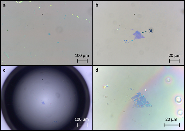
Figure 3. Optical microscope image showing an isolated monolayer of WSe2, before (a), (b) and after (c), (d) mounting a SIL; the scale bar in (d) has been adjusted to account for the SIL's magnification.
Download figure:
Standard image High-resolution imageOptical properties of SILs on WSe2
To fully assess the performance of the SIL, PL intensity maps of the WSe2 monolayer (from figure 3) were taken both before and after mounting the SIL, the results are shown in figure 4. It is clear from figure 4 that there is a significant increase in magnification of the PL map between (a) and (b), due to the mounting of the SIL. The extra resolution this provides enables more detail to be captured in PL maps, making edges and intensity differences easier to see. It should be noted that the horizontal artefacts are due to the PL maps being interpolated, to enable a better comparison with the optical images. The observed increase in resolution arises not only due to the magnification of the flake, but also from a slight reduction of the laser's spot size. Theoretically, the increase in resolution from a h-SIL in μPL arises from a decrease in laser spot diameter, which is proportional to  (where n is the refractive index of the SIL) [19]. The laser acting as a plane wave will approximately project an airy pattern with a half-width at half-maximum of:

where n = refractive index of the volume above the TMDC, NAobj = numerical aperture of the μPL system and λ = excitation wavelength [13]. Calculating (2) with the experimental parameters here gives an expected resolution increase of 1.6 times. The value measured from figure 4 is slightly larger than this, at 1.8 times, this discrepancy is attributed to the SIL having a contact angle to the substrate greater than 90°. The overall improvement in magnification is thus somewhere between that of an h-SIL (linear dependence with n) and an s-SIL (quadratic dependence with n) [19]. This result shows that SILs in between the h and s-SIL geometries can give optical properties that are a combination of the two, with the studied SIL showing a greater magnification than an h-SIL without introducing strong chromatic aberrations. This suggests that gradually increasing the contact angle to the substrate from 90° will change the magnifications dependence on refractive index from a reciprocal to an inverse square relationship. This means that epoxy SILs have the potential to be formed into geometries that can provide optimised trade-offs between resolution and image quality.
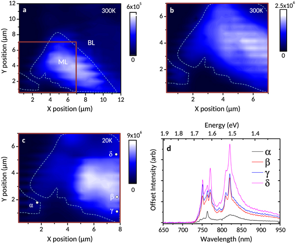
Figure 4. Photoluminescence (PL) maps of a WSe2 flake (outlined) taken both with and without a SIL and at low (20 K) and high (300 K) temperatures, as labelled; panels (a)–(c) show PL maps where the colour scale refers to the integrated intensity as a function of position; (d) shows example spectra from positions labelled in (c). The orange box in (a) highlights the area seen in (b) and (c).
Download figure:
Standard image High-resolution imageFigure 4(c) shows a map taken at cryogenic temperatures (20 K); it can be seen that the temperature change has had no detrimental effect on the optical properties of the SIL, or flake. This result shows that the SILs are highly resistant to temperature changes, and can thus be used for PL studies at cryogenic temperatures. Some example spectra from (c) are shown in figure 4(d), these correspond to areas where there was some overlap between monolayer and bilayer, as observed by the two main peaks. Sharp exciton-like lines can be observed in each of these spectra, this is unusual as these sharp peaks do not appear anywhere else on this flake, nor do they appear at room temperature. Since these peaks all occur at the same wavelength, it is unlikely that they are due to quantum dots, but could be due to defects/impurities that are more likely to occur at the monolayer-bilayer boundary.
When comparing figures 4(a) and (b) there is a significant increase in the intensity of light collected across the sample, with the integrated intensity increasing on average by 4.0 times for the same excitation power. Figure 5(a) shows the measured PL spectra of the flake from a single point in maps 4(a) and (b) (before and after the application of the SIL), the fourfold enhancement in the integrated intensity is easily observed as a large increase in the peak intensity. It was noticed that the relative enhancement varied with excitation power, this is shown in figure 5(b) where the ratio between SIL to no SIL is plotted versus excitation power for different monolayer positions. The measured PL enhancement was twice as high as predictions from classical optics, using equation (1) and extrapolating into solid angles. This increased enhancement could arise from constructive interference or confinement effects at a microscopic level, which cannot couple into the collection optics without a SIL. Simulating and quantifying these interactions is challenging due to the monolayer and the silicon dioxide substrate having dimensions that place the system into a semi-classical regime, making it computationally difficult. However, despite not being fully able to model the interactions, other emission increasing mechanisms such as doping of the sheet due to the epoxy can be discounted, as similar WSe2 monolayers show no enhancement in their PL when they are coated with a film of cured epoxy, rather than a SIL (figure 6).

Figure 5. Graphs showing (a) example PL spectra for monolayer WSe2 at 300 K excited using a 10 μW laser both with and without a solid immersion lens (SIL); (b) the power dependence of the ratio in PL intensity of SIL to no SIL for three different positions on the monolayer.
Download figure:
Standard image High-resolution image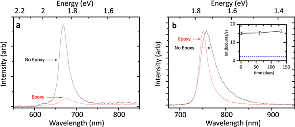
Figure 6. PL spectra of (a) MoS2; and (b) WSe2 before and after the application of a thin film of cured epoxy; inset graph demonstrating the lack of degradation through aging due to the epoxy, the dashed blue line shows the peak intensity before application of the SIL.
Download figure:
Standard image High-resolution image
The decrease of the intensity ratio with power is likely explained by the reduction in PL laser spot size with the presence of the SIL, and subsequent increase in power density exciting the monolayer. The increase in power density from the smaller spot size can reduce the relative PL intensity through charge screening effects, leading to a reduction of relative intensity with power. A decreased spot size could also cause an increase in localised heating of both the epoxy and the flake, which may affect both the emission of the monolayer and the optical properties of the SIL due to thermal effects.
Optical properties of SILs on MoS2
SILs were also mounted on top of MoS2 monolayers to see if they could be used to enhance the optical properties of the device in a similar fashion as for WSe2. Upon mounting a SIL, the emission of the monolayers was found to be heavily suppressed, and to investigate why, a 1.5 μm thick layer of epoxy was spin-coated onto the samples containing both types of monolayer. PL spectra from these samples are compared in figure 6, where it can be observed that there is a significant reduction in PL intensity for the epoxy on MoS2, with an accompanied red shift in the central wavelength. On the WSe2 no significant change in the peak intensity was observed, however the central wavelength blue-shifts, which is accompanied by a narrowing of the peak. The shift of the WSe2 peak and its sharpening are possibly attributed to a change in the proportion of emission from charged excitons, causing a reduction in the monolayer peak intensity at longer wavelengths. This would indicate that the monolayer WSe2 can be doped by the epoxy. The effects of doping also allow us to explain the results observed for MoS2. The mechanically exfoliated MoS2 is known to be naturally n-type [22], and it has been previously reported by Li et al in [23] that additional n-type doping results in a quenching of the PL. Thus, the epoxy bonded to the flake may be introducing dopants that result in the observed reduction in PL. MoS2 monolayers are highly sensitive to doping, with similar effects being reported to occur between MoS2 monolayers and the substrate that they are placed on [24].
The UV curing process of the epoxy may also induce compressive strain, influencing the optical properties of TMDCs. It has been shown that compressive strain can change the bandgap of MoS2 from direct to indirect [25], which would decrease the emission intensity. The compressive strain values needed to induce a shift from direct to indirect bandgaps for MoS2 and WSe2 are 0.5% and 1.5% respectively [26]. Since the threshold for WSe2 is higher than MoS2, the epoxy may have induced enough compressive strain to change the bandgap in MoS2, but not in WSe2.
It was hypothesised that, in addition to the improved optical properties, the SIL may also increase the longevity of TMDC monolayers in ambient conditions. Gao et al in [27] showed that under ambient conditions monolayer TMDCs degrade due to oxidation and the introduction of organic contaminants, but they themselves demonstrated encapsulation in transparent polymers can help prevent this. In our experiment over a time period of six months, there was no significant change observed in any of the encapsulated monolayers, despite being left in ambient conditions. Furthermore, the PL spectra's peak intensity remained almost identical for the same excitation powers, demonstrating that no degradation occurred during the time period. This can be observed in figure 6(b) (inset) where, within the uncertainty of the PL system, the intensity remained constant.
Conclusions
In conclusion, we have shown that UV-curable epoxy based solid immersion lenses (SIL) can be used to greatly increase the PL intensity collected from WSe2 monolayer sheets, with the measured intensity increasing by 250%–300% at low excitation powers. This was higher than theoretically expected, and several explanations for this were explored. The magnification provided by the SIL was found to be approximately 1.80 times, enabling PL maps to be produced with a higher resolution. This enhanced magnification and resolution could be of use in the optical analysis of WSe2, allowing for more details to be observed, and collection optics to be simplified. Conversely, MoS2 showed a quenching in the PL when the epoxy was incorporated. It is likely that the epoxy is either chemically altering the sheet or introducing compressive strain, however the mechanism behind this was not elucidated in this study.
Epoxy SILs are an excellent enabling technology for WSe2 based optoelectronic devices such as LEDs. The SILs should increase the optical coupling efficiency of these structures by at least 100%, but with a perfect s-SIL potentially up to 400%. The great advantage of this increase in light extraction is that it will interact in an accumulative manner with any other emission increasing methods, e.g. photonic crystal cavities [28], or plasmonic structures. This makes the epoxy SILs an important component for achieving close to unity input/output coupling efficiency for this type of device. Furthermore, SILs can help protect monolayer devices from degradation in air and the epoxy's insulating properties mean that it should have very little influence on the electrical properties of the LED. Overall, epoxy SILs are an incredibly promising optical package for the future of WSe2 based optoelectronics.
Methods
Sample preparation
Monolayers were mechanically exfoliated [29–31] from natural/synthetic bulk crystals of MoS2/WSe2 respectively, and transferred to the surface of silicon wafers with a 290 ± 5 nm SiO2 coating (this process is illustrated in figure 2(a)). An optical microscope was then used to identify individual monolayer flakes [32], which was additionally confirmed by observing the unique spectral signatures in the μPL spectra [33].
Optical characterisation
To analyse the optical properties of individual monolayers, the samples were placed in an evacuated cryostat and excited with a 532 nm CW laser through a 50× IR microscope objective lens with a NA of 0.65. PL was collected from the sample at 300 and 20 K through the same objective lens and passed through a single-stage spectrometer to a silicon EMCCD detector for wavelength-resolved measurements. The microscope objective was mounted on a piezo-driven XYZ stage with 20 nm step resolution, to produce PL maps as a function of position on individual monolayers.
Acknowledgments
RJY acknowledges support by the Royal Society through a University Research Fellowship (UF110555). This material is based upon work supported by the Air Force Office of Scientific Research under award number FA9550-16-1-0276. This work was also supported by grants from The Engineering and Physical Sciences Research Council in the UK (EP/K50421X/1 and EP/L01548X/1).
Competing financial interests
The authors declare no competing financial interests.
Author contributions statement
CSW & RJY designed the project. CSW fabricated the SILs, CSW, JR and YJN gathered and analysed the experimental data. AK provided exfoliated samples of 2D materials. The manuscript was primarily prepared by CSW, JR and RJY, with all remaining authors contributing to the pre-submission review of the manuscript.