

Abstract
We demonstrate a simple, scalable approach to achieve encapsulated graphene transistors with negligible gate hysteresis, low doping levels and enhanced mobility compared to as-fabricated devices. We engineer the interface between graphene and atomic layer deposited (ALD) Al2O3 by tailoring the growth parameters to achieve effective device encapsulation whilst enabling the passivation of charge traps in the underlying gate dielectric. We relate the passivation of charge trap states in the vicinity of the graphene to conformal growth of ALD oxide governed by in situ gaseous H2O pretreatments. We demonstrate the long term stability of such encapsulation techniques and the resulting insensitivity towards additional lithography steps to enable vertical device integration of graphene for multi-stacked electronics fabrication.
Export citation and abstract BibTeX RIS

Original content from this work may be used under the terms of the Creative Commons Attribution 3.0 licence. Any further distribution of this work must maintain attribution to the author(s) and the title of the work, journal citation and DOI.
As many graphene-based electronic and optoelectronic device concepts begin to make the transition from the research laboratory into real world applications [1, 2] it is imperative that factors such as long term stability and large area reproducibility are addressed. Graphene is inherently highly sensitive to environmental factors such as ambient air [3–5], lithography resists and polymers used in the transfer process [6] which cause unintentional, generally p-type, doping and hysteretic [7–10] behaviour in field effect devices. To overcome these issues device encapsulation and passivation is required.
Encapsulating graphene field effect transistors (FETs) with Al2O3 barrier layers deposited by atomic layer deposition (ALD) can significantly reduce gate hysteresis and provide reproducible performance over several months [10]. For graphene electronics, the potential advantages of such an encapsulation are two-fold. Firstly, Al2O3 is increasingly used as a moisture barrier in applications which require air sensitive materials, such as organic electronics, due to its exceptionally low water vapour transmission rate even for sub-100 nm films [11]. This leads to long term stability and protection of devices from humidity and other atmospheric effects. Secondly, the ALD process has been shown to effectively passivate charge trap sites such as silanol (SiOH−) groups at the SiO2—graphene interface [10, 12] which are responsible for much of the observed unintentional doping and hysteretic device behaviour [9, 10, 12–16]. However, due to weak out-of-plane interactions in graphene, achieving a high quality 2D––3D interface is a challenge which must be addressed to realise device integration with common dielectrics. Growth of ALD dielectric films on graphene is commonly achieved through an additional ex situ process step to promote nucleation, typically including deposition of an additional seed layer such as thin polymer [17, 18], metal/oxide [10, 19, 20] films, or other surface functionalisation pretreatments [21–24]. Such ex situ treatments may include time-consuming additional process steps, can degrade the quality of the graphene [20] and crucially may compromise the quality of the interface by introducing additional surface states. The effectiveness of the resulting encapsulation has been shown to be strongly dependent on the quality of this interface including diverse factors such as the oxidation state of the seed layer [10] and the microstructure of the graphene [25]. Recently, in situ pretreatments, such as exposing graphene to pulses of H2O [26, 27], O3 [28–31] or trimethylaluminum (TMA) [32], have shown promise in promoting uniform ALD of thin dielectric films. Most of these nucleation engineering studies have focused on process optimisation towards factors such as film coverage and density, however the impact and suitability of these in situ pretreatments for real device encapsulation has not yet been studied in detail.
By using H2O or O3 exposure in situ to act as a gaseous pretreatment to promote nucleation of Al2O3 directly on graphene during early ALD growth, followed by dense film growth after nucleation, we show near complete surface passivation of graphene FETs with enhanced mobility, reproducibility and long term stability. We show that ALD nucleation and the choice of in situ pretreatment dramatically alters final device performance, highlighting the importance of both the graphene—Al2O3 interface quality and the passivation of charge traps in the underlying gate dielectric during ALD. Finally, we show that the resulting encapsulation makes the graphene layers insensitive to additional lithography and processing steps which allows multiple levels of graphene devices for multifunctional vertical device integration.
Results and discussion
Figure 1(a) schematically shows the process of our ALD device encapsulation. Initially a wafer containing an array of globally back-gated two terminal CVD graphene channels on doped-Si/SiO2 (dielectric thickness tox = 300 nm) was fabricated by e-beam lithography, using oxygen plasma etching to define channels with a length and width of L = W = 10 μm, respectively, and sputtered Ni (70 nm) contacts. The field effect characteristics of a typical as-fabricated device are shown in figure 1(b) where the graphene channel conductivity σ is related to the current Id by σ = (L/W)*(Id/Vsd), with applied source-drain voltage Vsd = 10 mV unless stated otherwise, which is plotted as a function of gate electric field EBG = VBG/tox. The gate voltage is swept from negative to positive values (up sweep) and then back to negative values (down sweep) with a rate of dEBG/dt = 0.37 MV cm−1 s−1 (dVBG/dt = 11 V s−1). In line with previous literature at room temperature and under ambient conditions significant unintentional p-type doping is observed where the conductivity minimum associated with the charge neutrality point ECNP is observed at high positive gate voltages [16]. For the device shown in figure 1(b) we measure a peak field effect hole mobility μh, for the up sweep, to be 620 cm2 V−1 s−1. Such a value is typical for polycrystalline CVD films [33], the grain size here being ∼10 μm as determined by scanning electron microscopy (SEM) [25], and it is important to note that this two-terminal mobility value is reduced by including contact resistances [19].
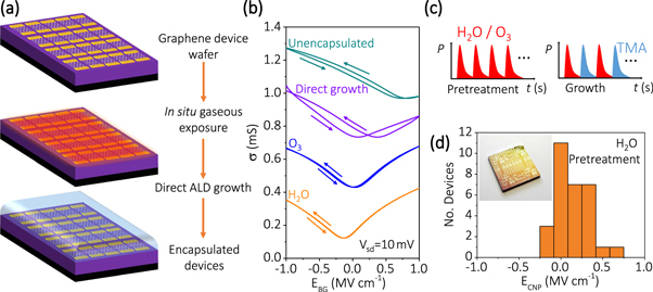
Figure 1. (a) Schematic of process flow for ALD encapsulation of graphene devices. (b) Comparison of unencapsulated (green) graphene FET characteristics with those encapsulated with 90 nm of Al2O3 using direct growth (purple), O3 (blue) and H2O (orange) pretreatments, respectively. Blue, purple and green curves are offset vertically by 0.3, 0.6 and 0.9 mS, respectively. (c) Schematic of ALD pulse sequences for the pretreatment and subsequent growth processes showing the chamber pressure P as a function of time t. (d) Distribution of Dirac point (ECNP) for 30 devices after encapsulating with an H2O pretreatment. Inset: an optical micrograph of the 1 cm2 encapsulated chip.
Download figure:
Standard image High-resolution imageFor a number of device applications ambipolar transport in graphene devices is desirable. As such, the unipolar (p-type) behaviour observed in as-fabricated devices needs to be converted to ambipolarity and, importantly, this must be stable during device operation and storage in ambient conditions. Hence, we tune the ALD encapsulation layers using three different growth conditions to determine the interface quality required for stable ambipolar device performance. The total thickness of the Al2O3 was kept constant at 90 nm for all samples to separate interface effects from water vapour/atmospheric transmission effects. The three growth conditions were as follows: (1) direct deposition of 90 nm Al2O3 at 120 °C using H2O/TMA precursors; (2) a pretreatment of ten pulses of O3 followed by 10 nm growth of Al2O3 interface layer using O3/TMA at 80 °C followed by an additional layer of 80 nm using H2O/TMA growth at 120 °C; (3) a pretreatment of ten pulses of H2O at 120 °C followed by 90 nm of growth using H2O/TMA precursors at 120 °C, as shown schematically in figure 1(c). During pretreatment the oxidant pulse and purging time were the same as those of the subsequent growth. Consequently, the pretreatment time is typically on the order of a few minutes. The ten pulses of both the oxidants during pretreatment were selected to achieve sufficient surface saturation on graphene to promote nucleation, based on previous reports [26, 31]. A detailed study of the parameter space of gaseous pre-treatments and their effects on nucleation can be found in [27]. For long term stability the barrier properties of the encapsulating ALD layer is crucial to obtain low gas transmission rates which would begin to affect the graphene over time [11]. Hence, devices were encapsulated with 90 nm of Al2O3 which has been demonstrated to be sufficient to enable long term stability [10]. We stress, however, that if the barrier properties of the film are further optimised this thickness requirement is likely to be reduced. To obtain ambipolar behaviour with minimal residual doping the deposition temperature was kept to 120 °C, as higher temperatures have been shown to result in n-type devices [34]. During O3 exposure the temperature was kept to 80 °C to prevent damage to the graphene [29, 35].
Figure 1(b) summarises the electronic performance of these three encapsulation techniques which are found to have a significant effect on the graphene—oxide (2D—3D) interface. Electrical transport measurements were taken under ambient conditions following a further lithography step to expose and etch through the Al2O3 above the probing pads as detailed in the methods section. For direct deposition without pretreatment we observe some reduction in residual doping levels and an increase in mobility to μh = 830 cm2 V−1 s−1. However, significant hysteresis of ΔECNP = 0.3 ± 0.085 MV cm−1 is still observed, where we define ΔECNP = ECNP(down) − ECNP(up). Using a simple capacitor model, with the gate capacitance per unit area CG, we can estimate the corresponding change in carrier density due to trapped charges to be Δn = CG tox ΔECNP/e = 6.5 × 1011 cm−2. This suggests that a large density of trap states remain at the interface after the encapsulation. In contrast, the device characteristics for the two encapsulated samples using gaseous pretreatments are dramatically different with minimal hysteresis. Indeed, for the H2O pretreatment we observe a highly reproducible average residual doping level of 3 × 1011 cm−2 (p-type), with a standard deviation of 4 × 1011 cm−2, as shown for 30 devices in figure 1(d). Some devices show low levels of n-type doping due to negative charges in the Al2O3 matrix [36]. Importantly, levels of hysteresis are significantly reduced to 0.033 ± 0.085 MV cm−1 and 0.017 ± 0.085 MV cm−1 for O3 and H2O pretreatments, respectively. For the H2O pretreated encapsulation this corresponds to a remarkably low hysteresis induced by carrier trap density of Δn ∼ 3.6 × 1010 cm−2. This value is comparable to the best performance devices reported in [10], but achieved while halving the number of encapsulation process steps. Similarly, [8] achieved comparably low levels of hysteresis using short (≤1 μs) gate pulses whereas our measurements are performed under DC conditions. In addition, the values of μh for the devices shown in figure 1(b) increase to 920 cm2 V−1 s−1 and 950 cm2 V−1 s−1 for O3 and H2O pretreatments, respectively. This mobility improvement can be linked to the reduction in charge traps in the vicinity of the graphene as such charged interface states are known to act as scattering centres [37]. Further improvements of mobility can be obtained through increasing the grain size of the graphene film (figure S1) [25]. Thus, in particular for the H2O pretreated sample, the up and down sweeps are almost indistinguishable. We can therefore conclude that the growth of 90 nm of Al2O3 directly on graphene using an H2O pretreatment can provide thorough passivation of graphene FETs and almost doping-free ambipolar behaviour whilst maintaining, or indeed enhancing, carrier mobility under ambient conditions.
As reported previously [7] the level of hysteresis is strongly dependent on a number of measurement factors, in particular gate sweep rate and sweeping voltage range (sweep magnitude). By observing the hysteresis in graphene FETs under pulsed electrical measurements it has been shown that when gate voltage pulses are applied shorter than the characteristic trapping time constants of interface traps, typically ≤1 μs, hysteresis is suppressed [8]. This characteristic trapping time constant also results in a sweep rate dependence of DC measurements which is often particularly strong in the commonly used device testing regime [7–10]. Figure 2(a) shows a comparison of the sweep rate dependence of hysteresis for encapsulated graphene devices using the three processes described above. The sweep rate was varied, dEBG/dt = 0.01–0.74 MV cm−1 s−1 (0.3–22 V s−1), by maintaining a constant step size and sweep magnitude of 3.33 MV cm−1 (VBG = ±50 V) whilst varying the time delay between steps. As expected, hysteresis decreases with increase in sweep rate. Device encapsulation using direct deposition results in large hysteresis (ΔECNP = 0.7–0.5 MV cm−1) and is found to be strongly dependent on sweep rates below 0.24 MV cm−1 s−1. By comparison the O3 pretreated encapsulation provides a reduced level of hysteresis where ΔECNP = 0.3–0.1 MV cm−1, however this remains strongly rate dependent at low sweep rates. Once again, the H2O pretreated encapsulation enables the lowest levels of hysteresis, down to just ΔECNP = 0.07–0.03 MV cm−1, which is only very weakly rate dependent. Note that whilst the magnitude of the hysteresis changes depending on the interface the relative frequency dependence is similar for all the processes, indicating the same type of charge traps are involved [12]. Using a fixed sweep rate of 0.133 MV cm−1 s−1 (4 V s−1), figure 2(b) shows that these trends continue as we vary the sweep magnitude. The most striking example is from the direct growth encapsulation where at large magnitudes the Dirac point hysteresis spans almost a quarter of the voltage range. The O3 and H2O pretreated encapsulations provide a greatly reduced variation, consistent with a lower density of charge trap sites.
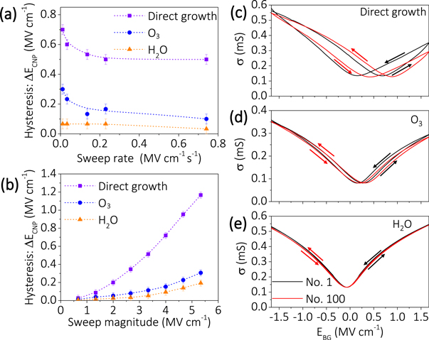
Figure 2. Dependence of hysteresis ΔECNP on (a) gate sweep rate with a fixed sweep magnitude of 3.33 MV cm−1 (−50 V ≤VBG ≤ 50 V) and (b) sweep magnitude using a fixed sweep rate of 0.133 MV cm−1 s−1 (4 V s−1). Dashed lines are guides to the eye. Device stability test showing the first and last measurement of 100 successive gate sweeps for graphene devices encapsulated with 90 nm Al2O3 using (c) direct growth, (d) O3 and (e) H2O pretreatments.
Download figure:
Standard image High-resolution imageThe presence of charge traps in the vicinity of graphene and its effect on the device performance is closely linked to reliability and reproducibility. We have investigated the device characteristics for a number of successive measurement cycles in order to quantify this effect and compared the advantages of optimised gaseous pretreatments on device stability. Figures 2(c)–(e) shows the first and last of 100 successive measurement cycles over the course of 30 min in ambient conditions for each encapsulation technique. Encapsulation using direct deposition, in addition to pronounced hysteresis, shows a substantial difference in the device characteristics and deterioration in the performance between sweep 1 and sweep 100 (figure 2(c)). A large shift in ECNP is observed over time equivalent to an effective carrier density change of n100 − n1 ∼ 6.5 × 1011 cm−2. Such an effect is rarely commented on in the literature to date but is clearly highly undesirable for any applications requiring reproducible stable device characteristics over a number of measurement cycles. While the levels of hysteresis and device stability is greatly improved using O3 pretreated encapsulation, a smaller but still finite shift of n100 − n1 < 1 × 1011 cm−2 is observed. No shift in ECNP is observed within measurement uncertainties for the H2O pretreatment over 100 measurements. This emphasises the potential for H2O pretreatments in ALD growth to achieve stable and reproducible graphene device characteristics.
Clearly the ultimate quality of the device is strongly linked to the quality of the SiO2–graphene–Al2O3 interfaces. To gain a more in depth understanding of these interfaces and the role of gaseous pretreatments we probed the nucleation of Al2O3 during the first few nm of growth. It is important to note at this point that the three growth conditions we have focused on are representative of a rich parameter space offered by ALD [27]. As a model system we study nucleation of Al2O3 on the surface of highly oriented pyrolytic graphite (HOPG). Wetting on the pristine surface of graphite is notoriously difficult [38]. On the other hand graphene grown by CVD and transferred using polymer support layers typically has grain boundaries, wrinkles and sources of contamination which should assist wetting and hence ALD nucleation. In addition, it has been shown that the wettability of CVD graphene is strongly dependent on the supporting substrate [38] and air exposure over time [39], thus we take mechanically exfoliated HOPG, within minutes of exfoliation, as the extreme case. Figure 3 shows the schematic nucleation replicas we follow based on SEM images of a nominally 2 nm thick deposition (20 ALD cycles) of Al2O3 on thick (>100 layer) mechanically exfoliated HOPG on an SiO2 substrate using direct growth, or O3, H2O pretreatments as shown in figures 3(b)–(d), respectively. Following direct deposition very sparse dendritic growth of Al2O3 is observed in the SEM as areas of light contrast in figure 3(b). We observe preferential deposition along energetically favourable step edges. Given that the O3 pretreatment ALD process is optimised to deposit nm scale thicknesses [31] we find, as expected, that this provides the highest overall coverage (figure 3(c)). However, across the sample areas of nanoscale pores can be seen which result in a relatively low overall film density. For H2O pretreated growth, a greatly improved coverage compared to direct deposition is observed (figure 3(d)). Due to the use of higher deposition temperature relative to O3 pretreatment, the areas which are covered are already showing the signs of dense film growth resulting in a much more complete passivation once full coverage is obtained.
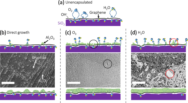
Figure 3. (a) Schematic for unencapsulated graphene showing the main contributions to the charge traps responsible for hysteresis. Scanning electron microscopy images indicate Al2O3 (light) on the surface of HOPG (dark) after nominally 2 nm of growth for (b) direct deposition, (c) O3 pretreatment and (d) H2O pretreatment. Schematics of ALD on graphene after ∼2 nm (top) and ∼10 nm (bottom) of growth. Circles indicate nano-porous (black) and dense (red) film growth for O3 and H2O pretreatments, respectively. Scale bars are 500 nm.
Download figure:
Standard image High-resolution imageWe can relate the three nucleation scenarios to the final device performance. In the first case of direct deposition very inhomogeneous growth results in a minimal passivation of SiOH− groups at the SiO2 surface. It assists in reducing the residual doping allowing observation of charge neutrality points within the operating voltages, but large hysteresis values are maintained. For the O3 pretreatment, a strong reduction in hysteresis is observed, although a complete surface passivation is not achieved in spite of the relatively homogeneous nucleation. During the pretreatment, the O3 carries along a significant amount of O2 which, in the presence of trace amounts of H2O, will drive the O2/H2O redox reaction toward reactive hydroxide species:  In addition, the use of O3 as oxidant in ALD has been known to result in oxygen-rich Al2O3 layer due to the presence of formate and carbonate species from incomplete reactions [40–42], which may later decompose into hydroxyl species and act as additional charge trap sites at the top interface. While a denser and more stoichiometric interface layer could be obtained at 120 °C, this may create defective graphene [29, 35]. Furthermore, the presence of nanoscale pores in the interface layer prevents complete surface passivation. On the other hand, the lower hysteresis obtained by H2O pretreatment may first appear counterintuitive as H2O increases the surface concentration of SiOH− groups on SiO2 surface [43] and at 2 nm the coverage of H2O pretreatment growth is incomplete. However, surface saturation by H2O drives the O2/H2O redox reaction toward H+ leading to the depletion of reactive hydroxyl and peroxide species [34, 44]:
  In addition, the remaining hydroxyl species are consumed more readily by TMA than the formate species [41], resulting in further removal of charge trap sites.
To demonstrate the advantages that this optimised approach for device manufacturing we fabricate a vertically integrated device stack, i.e. two levels of devices on the same chip which may operate either independently or in communication with one another, a concept outlined in figure 4(a). Without appropriate encapsulation, transferring another layer of graphene on top of a set of devices and performing several additional lithography steps will severely deteriorate the properties of the underlying graphene. We begin with a set of globally gated graphene devices encapsulated using 90 nm of H2O pretreated Al2O3. After testing (figure 4(b)), a second layer of CVD graphene is transferred. A top layer of devices was fabricated both in isolation, for modulation using the global back gate as in figure 4(c), and layered directly above the initial devices such that interlayer gating was possible (figure 4(d)). The top layer of graphene devices was then encapsulated with a further 90 nm of H2O pretreated Al2O3. Figure 4(b) shows that even after 2 months and several processing steps the bottom encapsulated layer of graphene shows only a minimal shift in ECNP from slightly n-doped to almost undoped, and no significant change in μ. Figure 4(b) and c shows that each layer has a ECNP close to 0 MV cm−1 and very low hysteresis values consistent with the results described above. Additionally, we can use the vertical device structures to have a graphene-gated graphene FET shown in figure 4(c). Perhaps the most exciting possibility enabled by this technique is to manufacture interlayer devices where, for example, within the same footprint in a chip multiple functionalities can be contained (figure 4(a)). By taking advantage of ambipolar transport in both layers, a combined graphene FET and inverter vertical device structure is realised as shown in figure 4(e). As expected, inverting voltage characteristics were obtained indicating that the graphene in the vertical structure maintains the homogeneity and low doping suitable for device operation [45, 46]. These results highlight that H2O pretreated Al2O3 deposition not only achieves a high quality graphene—oxide interface but that the barrier properties of the Al2O3 film are sufficient to allow long term stability under common lithography conditions.

Figure 4. (a) Illustration of multiple levels of graphene devices for multifunctional vertical device integration. As a proof of concept we fabricate a vertical device stack consisting of a large CVD graphene channel on Si/SiO2 with Ni contacts encapsulated with 90 nm of H2O pretreated Al2O3, on top of which is fabricated another CVD graphene device, which is encapsulated with a further 90 nm of H2O pretreated Al2O3. (b) Transfer characteristics of the bottom device layer after 2 months, a wet graphene transfer, and three additional lithography steps. The device characteristics of isolated devices from the (b) bottom and (c) top encapsulated graphene layers using the global Si/SiO2 back gate as shown schematically (right). (d) In a vertical device structure the bottom layer of graphene is successfully used as a local gate to modulate the top graphene layer. (e) Inverter characteristics of the interlayer vertical device stack shown in the optical micrograph (right) where the bottom (black dotted line) and top (blue) graphene layers are highlighted for clarity.
Download figure:
Standard image High-resolution image
Discussion
The advantages of ALD oxides for device encapsulation are widely accepted and routinely employed at an industrial scale. Process parameters were adjusted, for example in organic light emitting diode and photovoltaic applications, by considering the specific requirements of the active materials, i.e. organic semiconductors or Si respectively. So it is that for graphene, being a relatively new 2D material facing unique integration challenges such as its extremely high surface-area-to-mass ratio, these ALD processes parameters need to be understood and refined following a material specific methodology. Initial success has been achieved in past few years by the assistance of ex situ nucleation sites on graphene. Specifically, 2–3 nm of metal and metal oxide seed layers deposited by e-beam evaporation have been shown to be highly effective, but this additional process step spans several hours, a time which is equal to the growth time of a high quality ALD oxide layer. This also typically involves the devices being transferred from vacuum to ambient conditions, potentially compromising the quality and reproducibility of the interface. Hence, in the present study we use gaseous oxidant species as in situ pretreatments to promote nucleation within the ALD chamber and achieve a one-step encapsulation process. Previous reports [26, 31] have used H2O and O3 pretreatments, respectively, and discussed their importance in obtaining uniform coverage of Al2O3. In the present study, we carried forward this concept to determine their compatibility for large area CVD monolayer graphene devices, where we show the clear benefits of using H2O over O3 pretreatments for SiO2 supported graphene and device encapsulation. The time required for the gaseous pretreatment was only a few minutes, which makes it highly scalable with fast processing compared to many ex situ pretreatments [10]. The doping, hysteresis and charge trap density values obtained here are amongst the best in the literature showing that neither the quality of graphene nor the encapsulation layer was compromised. It is worth noting that we achieve this effective encapsulation whilst using comparatively small grain size graphene with a polymer supported transfer technique and despite having no additional cleaning or annealing steps beyond acetone and isopropyl alcohol. The voltage sweep rate dependent study also revealed the cause of the hysteresis is due to same charge trap species as discussed in the literature and its removal and encapsulation can be stongly governed by the use of gaseous pretreatments. This may open new avenues for neuromorphic memory applications where researchers are seeking to obtain controllable, finite levels of hysteresis in graphene devices [47], but often struggle to achieve reproducible characteristics. Two layers of graphene device encapsulation were realised on the same chip, each showing the performance required for vertical device integration. Whilst we do not observe a voltage gain in the graphene gate-graphene channel integrated inverter, which is expected to be the case for graphene with such a thick oxide dielectric [45], the interaction between two layers of graphene demonstrates the feasibility of future 3D chip fabrication using graphene and other 2D materials.
To conclude, we have demonstrated a scalable and simple approach towards encapsulating and passivating high quality CVD graphene electronic devices by using a gaseous H2O pretreatment to allow direct ALD of dense Al2O3 films on graphene. Using this technique, contained within a single piece of equipment, we eliminate the additonal time consuming processing steps and tools required to deposit the metal or metal oxide seed layers most commonly used to promote ALD growth. The obtained graphene doping levels and DC hysteresis values are amongst the lowest values reported to date by any technique. Moreover, we also achieve the desired characteristics for multi-level, vertically stacked devices. These results highlight the importance of not only the quality of the ALD grown top dielectric but also the material specific choice of growth parameters required. We hope that this work will motivate further device performance enhancements for new generations of low dimensional materials by using in situ gaseous pretreatments within the large parameter space offered by ALD.
Methods
Graphene growth and device fabrication
Cu foil was initially slowly heated to 1065 °C in a mixed H2/Ar environment (50/200 sccm) at 100 °C min−1. Once the growth temperature was reached, the Cu foil was kept in H2/Ar (50/200 sccm) for 30 min Graphene was subsequently grown in an Ar/H2 gas environment (250/26 sccm) using 9 sccm of CH4 (0.1% diluted in Ar), for 45 min. Samples were cooled in 250 sccm Ar to room temperature. The total pressure at all process stages was 50 mbar. The graphene films were then transferred to 300 nm SiO2/Si wafer support using a wet transfer method with polymethylmethacrylate (PMMA) as sacrificial transfer layer and ammonium persulfate as Cu etchant. Electron beam lithography was used to fabricate devices using PMMA or MaN-2405 for positive and negative processes, respectively. After encapsulation a further lithography step was required to expose probing pads located away from the graphene channels which was subsiquently etched using phosphoric acid (64%) at 80 °C for ∼3 min.
ALD Al2O3 layer
90 nm Al2O3 was deposited by ALD (Cambridge Cambridge Nanotech Savannah S100 G1) using TMA (purity >98%, Strem Chemicals 93-1360) and deionized water (H2O) or ozone (O3, DELOzone LG-7, ∼90% power) that were delivered alternatingly into the reaction chamber by 20 sccm of N2 flow. The dose for TMA and H2O was ∼0.5 Torr⋅s, while the dose for O3 was ∼5 Torr⋅s, which is approximated by the product of the of the peak delivery pressure with the residence time (full width at half maximum) determined by the pressure profile. The purging time between pulses was 20 s.
Transport characteristics
Electrical transport measurements were acquired on Keithley 4200-SCS connected to a probe station. Mobility was calculated using, μ = (∣dσ/dVG∣max)/CG, where the gate capacitance is taken to be CG = 11.6 nF cm−2 for 300 nm SiO2.
Acknowledgments
This work was supported by the EPSRC (Grant Nos. EP/K016636/1, GRAPHTED and EP/L020963/1) and the ERC (Grant No. 279342, InsituNANO). JAA-W acknowledges a Research Fellowship from Churchill College, Cambridge. JS acknowledges support from NUDT. ZAVV acknowledges funding from ESPRC grant EP/L016087/1. ACV acknowledges the Conacyt Cambridge Scholarship and the Roberto Rocca Fellowship. RW acknowledges EPSRC Doctoral Training Award (EP/M506485/1).