

Abstract
(Sub)monolayer MoTe2 is grown by molecular beam epitaxy on a bulk MoS2 substrate. The film morphology, the thermally induced transformation of structural and compositional phases, as well as the chemical stability upon exposure to atmosphere are investigated by scanning tunneling microscopy and photoemission spectroscopy. Predominantly, semiconducting α-MoTe2 islands are obtained under tellurium rich growth conditions and a substrate temperature of 200 °C. Under less tellurium-rich conditions, elongated and meandering MoTe2−x strands are formed rather than compact islands. Similarly, annealing of initial α-MoTe2 islands to above 500 °C causes the loss of tellurium and possibly transformation into the same MoTe2−x strands. Consequently, under vacuum conditions the the transformation of α-MoTe2 monolayers into the semimetallic β -MoTe2 high temperature phase is accompanied by a loss of Te and formation of MoTe2−x phase. The obtained tellurium deficient MoTe2−x phase is almost metallic but a small band gap of a few tens meV remains. The as-grown α-MoTe2 islands exhibit a moiré structure with ∼2.6 nm periodicity. This periodicity implies a rotation of ∼56° between the MoTe2 and MoS2. We assign the observation of a specific rotation angle for the grown MoTe2 islands with respect to the MoS2 substrate to the lowest energy adsorption configuration for MoTe2 monolayers on MoS2 substrates. Exposure of the as grown films to atmosphere results in oxidation of the MoTe2 film. The oxidized film maintains the two-dimensional island morphology of the initial film and thus is a candidate for a 2D (amorphous) oxide layer on MoS2.
Export citation and abstract BibTeX RIS
1. Introduction
Mechanical exfoliation and stacking of different mono- to few layers of van der Waals materials on top of each other enables the creation of novel devices and materials [1–9]. The functionality of these materials also led to a renewed interest in directly growing van der Waals heterostructures by molecular beam epitaxy (MBE) [10]. Direct growth of these materials has the advantage of being a scalable process and enabling materials fabrication on a wafer scale. MBE of van der Waals materials has been initially explored in the 1990s [11–15]. During this time the benefits of relaxed lattice matching conditions due to the weak interlayer interactions appeared promising for growing heterostructures with a variety of properties. These studies also resulted in a number of fundamental materials characterization of such grown films. For instance, a transition from an indirect to direct gap for monolayer materials has been already observed in angle resolved photoemission (ARPES) in 2001 on such grown monolayers [16]. In order to make devices, or to characterize novel properties induced by interfaces, a better understanding or even just achieving the growth of various van der Waals materials is required. While growth by chemical vapor deposition (CVD) has accomplished the fabrication of heterostructures of different van der Waals materials [17, 18]. CVD growth is currently difficult to control and typically the reported results only represent a few well-defined islands over the entire wafer. Nevertheless these local heterostructures are very useful for fundamental materials characterization and prototype device characterization. Physical vapor growth or (MBE) is an alternative approach for van der Waals epitaxy [19, 20]. MBE potentially allows the fabrication of heterostructures on wafer-scales, which also enables surface and interface characterization by non-local techniques like ARPES. Generally, MBE has the advantage over other growth methods by allowing control over elemental deposition rates and easy switching from one material to another, thus in principle enabling precise control for heterostructure growth. A challenge for many van der Waals materials, such as transition metal dichalcogenides (TMDs), is that the deposited materials are volatile either in elemental form or as small molecules. This causes a low sticking coefficient on the growth-substrate, especially on inert van der Waals substrates. As a consequence, MBE generally requires low growth temperatures and chalcogen rich conditions.
In this communication we examine the growth and properties of (sub)monolayer MoTe2 on bulk MoS2 substrates. α-MoTe2 has a sub-1 eV band gap and thus is particularly interesting for infrared optical applications. MoTe2 has two well-known structural phases [21]. Both phases are van der Waals materials, i.e. structures with strong in-plane covalent bonding and weak interlayer interactions. The α-phase of MoTe2 is isostructural to MoS2 or MoSe2, i.e. it forms the hexagonal 2H-MoTe2 structure, with an in-plane lattice constant of a = 3.519 Å. This α-phase is semiconducting with an indirect band gap of 0.88 eV for the bulk material [22]. The β-phase, on the other hand, is a semimetal and has a monoclinic structure. The rectangular unit-cell of the monolayer has lattice constants of a = 6.330 Å and b = 3.469 Å. In the β-phase the Mo-atoms are displaced from the center-plane of the monolayer, giving rise to a buckled monolayer structure. Furthermore, the Mo-atoms form quasi-one dimensional zigzag chains along the b-direction. The reduced Mo–Mo separation along this chain gives rise to increased metal-metal interactions, which also causes strongly anisotropic conductivity. Figure 1, shows structural models for the two MoTe2 polymorphs. Historically, the phase transition from the α- to the β-phase was reported to occur between 820 °C and 880 °C [23], with the higher transition temperature for slightly tellurium depleted material (MoTe1.90). In a very recent paper the phase transition was revisited and much lower phase transition temperatures were found [24]. In this recent study the phase transition temperature was found to be significantly lower and dependent on small variations in the composition. For slightly Te-deficient materials the transition already started at ∼500 °C and for Te-enriched phase the α-phase was found to be stable up to 750 °C. Once transformed into the β-phase, this structure remains metastable to low-temperatures without transforming back into the α-phase, allowing its characterization at or below room temperature [25].
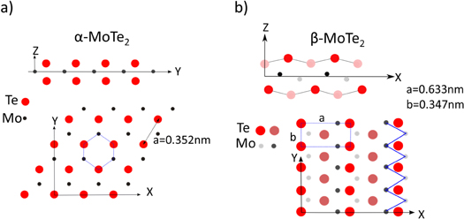
Figure 1. Cross-sectional and top-view schematics of (a) α-phase and (b) β-phase of MoTe2.
Download figure:
Standard image High-resolution imageSemiconducting to metallic phase transitions are also known to exist for other TMDs. However in these cases the structural transitions are induced by electron-donation. For instance in MoS2 a transition from the stable 2H or 3R structure to so-called 2T or 2T' structure is induced by Li-doping (Li is used in chemical exfoliation of these materials and thus metallic phases are often obtained in this process) [26–28]. This structural transition is similar to that of MoTe2 with respect that it increases Mo–Mo interactions in one crystallographic direction. Recently, it has been suggested to use this phase transition in MoS2 to pattern a MoS2 monolayer with metallic and semiconducting regions by inducing the phase transition locally [29]. Similar proposals may be made for MoTe2, where the metallic phase could be formed, for example, by local heating, rather than chemical charge donation. However, for achieving this on a wafer scale, uniform growth of α-MoTe2 is a prerequisite. Here we study the growth of MoTe2 on MoS2 substrates. We find that the obtained phase is strongly dependent on the growth conditions, especially the growth rate, with the desired α-MoTe2 phase only obtainable at extremely slow growth (monolayer in hours) and under tellurium rich conditions. Also, tellurium is easily lost from the film by vacuum annealing, resulting in a tellurium-deficient phase that remains planar but favors quasi-one dimensional morphologies. Importantly, this tellurium poor phase exhibits only a very small band gap and thus despite its fragmented morphology could still be used as an electric contact material. The structure of this phase may be related to the β-phase of MoTe2, which also exhibits quasi-one dimensional structures due to the formation of Mo–Mo chain structures.
For the α-MoTe2/MoS2 interface we observe the formation of a moiré-structure due to the different lattice constants between the monolayer and the substrate. This moiré structure indicates that the MoTe2 monolayer grows rotated by ∼56° relative to the MoS2 substrate. Finally, we point out that the films we have grown are unstable in air and easily oxidize. However, the formed MoO3TeO2 maintains the 2D-shape of the grown islands and thus this may be a useful approach for the formation of an ultrathin dielectric oxide layer on MoS2.
2. Experimental methods
The experiments are conducted in a UHV system consisting of a preparation chamber for MBE of chalcogenides and a surface analysis chamber. The preparation chamber is equipped with a K-cell for tellurium and a mini e-beam evaporator for Mo evaporation. The sample manipulator allowed for radiative, or e-beam heating of the substrate, which was mounted on a Ta-sample plate. The MoS2 substrate was a commercially available synthetically grown MoS2-single crystal from 2D Semiconductors Inc. The crystal was cleaved in air and subsequently annealed in vacuum at 300 °C for 4 h prior to the film growth. The cleanliness of the sample was checked by x-ray photoemission spectroscopy (XPS) and no contamination was detected. Impurity levels below the detection limit of the XPS (∼1%–2% of a monolayer) can, however, not be excluded. For film growth the K-cell for Te-evaporation was stabilized at 240 °C for 10 min. This K-cell temperature gave approximately a deposition rate of 0.05 nm min−1 determined by a quartz crystal monitor. The Mo deposition was measured with a built-in flux monitor and was kept constant during deposition. After stabilization of the sources the sample temperature was increased to growth temperature and subsequently the shutters of the deposition sources were opened and the sample rotated to face the deposition sources. The main interest in this study is samples grown on MoS2, however, for calibration and determination of oxidation-states we also grew a few samples on graphite (HOPG) under the same growth conditions. This was mainly done to avoid overlap of the Mo peaks from the substrate and the grown MoTe2 films. After completion of the growth the sample was transferred in situ to the analysis chamber with help of a magnetically coupled transfer arm. In the analysis chamber the sample manipulator was also equipped with a calibrated e-beam heater, which enabled heating of the sample to specific target temperatures by radiative or e-beam heating. The accuracy of the annealing temperature is estimated to ±40 K. The mu-metal analysis chamber was equipped with an Omicron Sphera-II electrostatic analyzer for photoemission spectroscopy. For XPS a Mg/Al dual anode x-ray source and for ultraviolet photoemission spectroscopy (UPS) a VUV He-discharge lamp was used. For the XPS measurements reported in this manuscript the Mg anode was used. The emitted photoelectrons were detected at an emission angle of 53° (measured from the surface normal) to increase surface sensitivity. For quantitative measurement of the MoTe2 composition we used MoTe2 grown on HOPG. The composition of the film was then determined from Mo/Te peak intensities taken the atomic sensitivity factors of the elements as well as the transmission function of our analyzer into account. For optimized preparation conditions we found 67 ± 3 at% Te and 33 ± 2 at% Mo in the grown films in agreement with MoTe2. Also, post-air exposure analysis of the oxidation state of Mo and Te was done on HOPG, as well as for Te on MoS2.
In addition, the analysis chamber also housed a room temperature scanning tunneling microscope (STM) (Omicron STM 1). Electrochemically etched W-tips were used. The STM was used for imaging and local I–V spectroscopy. dI/dV derivatives were obtained numerically. Scanning tunneling spectroscopy (STS) maps were acquired by taking I–V spectra at every data point and subsequently the measured tunneling current at these data points for specific bias voltages were plotted. STS maps enabled the identification of MoTe2 phases.
3. Results
3.1 . Direct MoTe2 growth
Submonolayer of MoTe2 is deposited by co-vapor deposition of Mo and tellurium on a heated MoS2 substrate. The film morphology is very sensitive to the growth rate and the Mo/Te ratio. For the case of growing MoTe2, where any excess Te re-evaporates from the surface, the growth rate is primarily determined by the Mo-flux. In this study we mainly modify the Mo-flux and thus a fast growth rate also corresponds to a higher Mo/Te flux ratio, while a slow growth also corresponds to Te-rich conditions. Growth temperature below 200 °C causes formation of 2D-islands with dendritic shape reminiscent of a fractal growth [30]. This is shown in figures 2(a) and (b). A dendritic or fractal growth is expected at low temperatures for which molecular species that attach to the island have not enough mobility to diffuse along the edges of the growing island to form an equilibrium island shape. Commonly one would expect that the dendritic growth of such islands could be overcome by increasing the growth temperature in order to increase diffusion and thus enable the formation of equilibrium island shapes. Unexpectedly, however, we observe a different growth behavior. With growth temperatures above ∼350 °C the islands become very elongated and form meandering islands, as shown in figure 2(c). Such a drastic change in growth is explained if the grown islands are of a different structural phase and/or composition. If such a different phase has strongly anisotropic edge energies, elongated islands may result as an equilibrium shape rather than compact island-shapes. Increasing the growth temperature does not only modify the surface diffusion but also decreases atomic/molecular residence times on the substrate. For example a preferential desorption of Te-species could result in a different composition of the grown film. Unfortunately, an exact measurement of the composition of the sub-monolayer films by XPS is made impossible because our substrate contains the same transition metal, i.e. Mo, as the film. Below, we show that annealing of α-MoTe2 islands also show a transition into quasi one-dimensional strands with a concurrent loss of Te and thus we assign both morphologies to the same fundamental MoTe2−x phase.

Figure 2. Initial nucleation and growth under low excess Te conditions for 15 min growth time and different substrate temperatures: (a) 25 °C (b) 200 °C and (c) 350 °C. Up to 200 °C the islands form a dendritic island shape indicating edge-diffusion limited island growth. Increasing the growth temperature to 350 °C does, however, not result in more compact islands under these conditions but elongated meandering islands are formed (c).
Download figure:
Standard image High-resolution imageIn order to obtain mainly α-MoTe2 the Mo-flux was reduced and the substrate temperature was held at T = 200 °C. The low Mo-flux resulted in a slow growth of ∼0.16 ML h−1 and Te-rich growth conditions. Under these conditions, growth of more compact islands was obtained. STM images of the morphology of these films are shown in figure 3(a) as a function of growth time. Under these growth conditions the island density does not increase with deposition time indicating that the nucleation density is determined by either defects in the substrate (heterogeneous nucleation) or the island density is given by the diffusion length of molecular species necessary for the formation of a stable nuclei. The latter implies a long diffusion length of the order of the island separation of 50–100 nm. A long diffusion length before the formation of a critical nuclei also explains that second layer islands are not observed until islands reach a size of the order of ∼35 nm in diameter. A detailed analysis of the growth mode will require more systematic analysis at different growth temperatures and deposition rates and is beyond the scope of the current communication. STS, shown in figure 3(b) indicate that the center of these islands are semiconducting with a band gap of approximately 1.03 ± 0.02 eV, however, some metallic regions are present at their perimeter. Closer inspection of the metallic region with atomic-resolution imaging indicates that these regions are β-MoTe2. The STM images shown in figure 3(c), show a rectangular unit-cell with dimensions matching the expected monoclinic unit-cell of β-MoTe2. Furthermore, the images compare very well with previously reported STM images of bulk β-MoTe2 single crystals [24]. The semiconducting regions are α-MoTe2 as the hexagonal atomic-structure of the atomically resolved regions, also shown in figure 3(c), indicates. The α-MoTe2 domains also exhibit a triangular superstructure. A similar structure was observed for MoSe2 grown on MoS2 and was associated with a moiré-structure due to the lattice-constant differences between the substrate and the monolayer film [13]. The observed 2.6 nm periodicity of the superstructure can be reproduced with the lattice constants of MoTe2 and MoS2 assuming that the two lattices are rotated by ∼56° with respect to each other, as discussed below. Here we define the rotational angle such that 0° rotation corresponds to exactly the same structure of two subsequent layers, i.e. in the typical 2H-structure of TMDs the rotation of subsequent layers would be 60° in this notation. The band gap determined by STS matches closely the value reported previously by optical measurements for monolayer MoTe2 [31]. This indicates that at least part of the MoTe2 film is similar to freestanding exfoliated MoTe2 monolayers, however, the question if the band structure is modulated within the moiré unit cell, as has been proposed for similar van der Waals heterostructures [32], require more detailed and higher resolution STS studies. The sample preparation discussed here should enable such studies in the future.
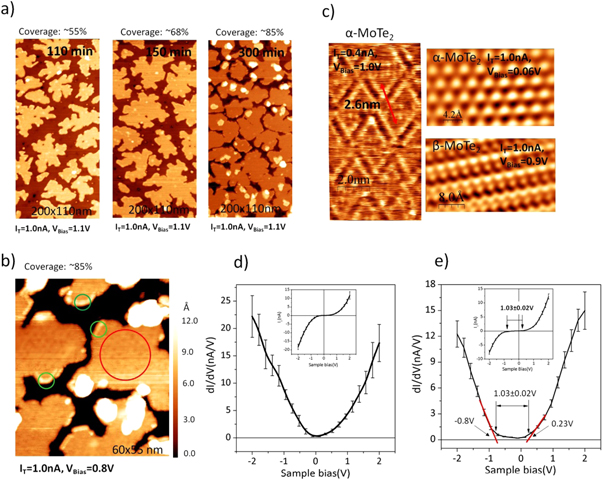
Figure 3. Characterization of MoTe2 (sub) monolayer island growth on MoS2 under increased Te excess deposition conditions and 200 °C substrate temperature. (a) Large scale STM images for different MoTe2 growth times on MoS2. Significant multilayer growth is only observed for 300 min deposition time when an almost complete monolayer is formed. Scanning tunneling microscopy image shown in (b) indicates the islands exhibit a moiré structure shown in more detail in (c). Furthermore, the center of the island (red circle in (b)) is α-MoTe2, as the atomic resolved STM images reveal. Some edges (green circles in (b)) of the islands that exhibit metallic properties can also be identified as β-MoTe2 by atomic resolved images. Scanning tunneling spectroscopy reveal that some edges exhibit a very small band gap (d), while for the α-MoTe2 monolayer a band gap of 1.03 ± 0.02 eV is measured in (e) with a VBM at 0.8 eV below the Fermi-level.
Download figure:
Standard image High-resolution imageUPS measurements of the grown films show a coexistence of a metallic and semiconducting phase. The metallic contribution can be reduced by annealing to ∼500 °C and reduced even further by covering the surface with Te prior to the annealing step. After annealing, all the excess Te is desorbed but the UPS spectra are better defined possibly indicating a reduction of defects and association of the metallic features with tellurium deficiency in the monolayer. The valence band spectrum for the MoTe2 film annealed to 500 °C can be found in figure 4(b) and shows the VBM of the α-MoTe2 phase to 0.78 eV, which is in reasonable agreement to the value of 0.8 eV determined by STS (see figure 3).
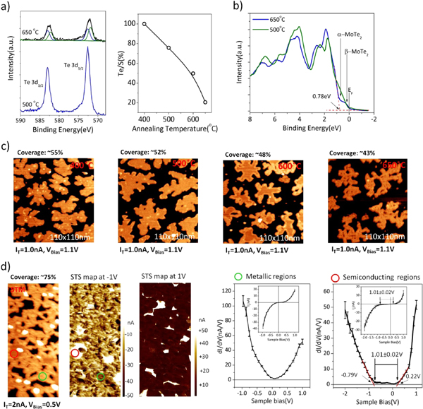
Figure 4. Transformation of sub-monolayer MoTe2 by thermal annealing. (a) Te-3d XPS and (b) UPS of submonolayer MoTe2 film annealed to 500 °C and 650 °C for 30 min. The film is stable up to 500 °C and no strong changes in XPS and UPS are observed, apart from a small Te-loss in XPS. Increasing the annealing temperature above 500 °C results in Te-loss and the Te-3d peak broadens which may be fitted by an additional lower binding energy component. (b) shows the UPS spectra with 0 eV binding energy corresponding to the Fermi-level. All our sub-monolayer MoTe2 films exhibit a metallic component for annealing temperatures below 500 °C. This shoulder is attributed to the minority β-MoTe2 phase while the main intensity increase corresponds to the valence band maximum of α-MoTe2. Annealing to 650 °C causes an increase in intensity closer to the Fermi-level corresponding to a more metallic character of the film. The change in electronic structure is accompanied by a morphology change observable in STM images shown in (c). With increasing annealing temperatures the islands shrink indicating desorption of both Te and Mo and thus partially explaining the strong decrease in Te observed in XPS. In addition, a transformation starting from the island edges is observed. At 600 °C most of the islands exhibit a bright edge which propagates inwards and at 650 °C all the islands are transformed. However, not a continuous island is formed but instead the islands exhibit many holes and consist of a dense network of strands. In (d) the electronic structure of a film grown under low Te-excess conditions is shown. Such films exhibit a morphology very similar to the post-growth annealed samples. Areas marked by a red-circle are non-transformed, semiconducting α-MoTe2, as the dI/dV curve indicates, while the dI/dV curves taken in the green circle show metallic behavior. Plotting STS-maps, i.e. taking I–V spectra at every data point and subsequently plot the measured tunneling current for a specific bias voltage, enables to identify all the metallic regions and all the remaining semiconducting regions, as well as regions that still expose the MoS2 substrate. In STS maps with −1 V bias the semiconducting regions appear bright, and for +1 V bias the MoS2 substrate regions exhibit the highest tunneling current and therefore appear brightest. The STS maps can be compared to the regular STM image to identify the corresponding regions.
Download figure:
Standard image High-resolution image3.2 . Morphology change in post-growth annealing
For stoichiometric bulk MoTe2 a transition from α- to β-phase is expected around 650 °C, however this phase transition temperature is reduced to only 500 °C for slightly Te-deficient samples [24]. Here we investigate if for sub-monolayer MoTe2 this phase transition occurs at the same temperature or other structures are formed. As mentioned above for annealing temperatures below 500 °C the MoTe2 islands are stable and seem to improve in terms of defect concentration from both STM and UPS measurements. The change in the UPS spectrum for MoTe2 for different annealing procedures is shown in supporting information (figure S1). It is apparent that width of spectral features become better defined after annealing which is a hallmark of lower defect concentration. At higher annealing temperatures XPS indicates, however, a loss of tellurium from the surface, as shown in figure 4(a). Some of the tellurium loss is attributed to desorption of MoTe2, which is evident from a shrinking of the island size observed in STM images (figure 4(c)) and discussed below in more detail. However, just evaporation of MoTe2 cannot account for all the loss, indicating also formation of sub-stoichiometric MoTe2−x. In addition to loosing tellurium from the surface, the tellurium peak develops a second component at ∼0.8 eV lower binding energy. A second component at lower binding energy suggests the presence of a chemically distinct tellurium specie with more negative charge, which may indicate a coordination-change to Mo atoms. In UPS measurements the valence band edges that we assigned to a superpositioning of α- and β-phases of MoTe2 for the as-grown film become 'smeared out' at elevated annealing temperatures, as is shown in figure 4(b). Thus no simple transformation from a predominant α- phase to a predominant β-phase is observed for vacuum annealing of sub-monolayer MoTe2 samples. Instead photoemission suggests annealing to the phase transition temperature is also associated with formation of a Te-poor phase. Electronically this phase may be best described by a high density of defect states that cause the formation of a poorly defined valence band edge and exhibits states up to the Fermi-edge.
STM studies elucidate the structural and phase transformations, which occur for annealing temperatures above 500 °C. Figure 4(c) shows a sequence of STM images as a function of annealing temperature. It is apparent that a transformation originates from the island edges at above 500 °C, which propagates towards the island center with increasing annealing time and temperature. In STM this transformation is visible by a brighter contrast of the transformed region. Such brighter contrast may be associated with a transformation to a metallic state and thus a higher tunneling probability in STM. After annealing at 650 °C for 30 min all the islands are completely transformed. In this transformation the morphology of the islands also is changed. Instead of a contiguous island, holes are formed and the new structure consists of elongated, quasi-1D sections that have a width of approximately 10.0 nm. This transformation is likely due to the loss of Te. At the annealing temperatures of ∼600 °C MoS2 is still quite stable and the intermixing of sulfur and tellurium will be minimal at these temperatures. The reasoning that this island morphology is a consequence of Te-loss during post-growth annealing is further supported by the fact that the same island morphology, i.e. a structure consisting of many elongated segments separated by holes, can be obtained by growing a film directly under less Te-rich conditions. Such a film is shown in figure 4(d). Furthermore, the straight segments may be related to the initial nucleation and growth of the elongated islands in figure 2(c), which we also attributed to a Te-poor phase. Because of these structural similarities we tentatively interpret all these elongated strands as the same MoTe2−x structure. The reason why an elongated features and even formation of holes in the islands rather than formation of compact islands are preferred may be related to the anistropic crystal structure of β- MoTe2. The chains of Mo-atoms in this structure (shown in figure 1) may result in an anistropic growth and more importantly results in a strongly anisotropic edge energy, causing long edges in the direction of the Mo-chains. To confirm that the island structure shown in figure 4(d) is mainly metallic, and thus more closely related to β- MoTe2, we performed, in addition to STM, also local STS spectroscopy. STS maps show the metallic and semiconducting regions in the film. It is apparent that all the regions that exhibit the strand-like structure are metallic and only small regions of semiconducting α-MoTe2 are present in this particular film.
3.3. Oxidation of MoTe2 films by air-exposure
Exposing submonolayer MoTe2 films to air results in an oxidation of the film. Ambient-air AFM images are shown in figure 5(a), which may be compared to STM images taken of the same film in UHV prior to air exposure, shown in figure 5(b). The island structure is maintained. Measuring the island height (see supporting information figure S3), however, reveals that island after air exposure are significantly taller (1.02 ± 0.06 nm) than expected for MoTe2 (0.6 nm). Subsequent characterization of the film by XPS shows that the Te peak shifts by 3.42 eV from 572.71 eV for MoTe2 to 576.13 eV, as shown in figure 5(c). The latter peak position corresponds to TeO2. To evaluate the Mo-3d peak positions after air exposure without having to de-convolute the contribution from the MoS2 substrate we also grew sub-monolayer of MoTe2 on HOPG-graphite. In these measurements, shown in figure S2, we observe a Mo-3d peak at 227.70 eV for MoTe2 and a shift to 232.36 eV after air exposure. The latter peak position is consistent with MoO3. Thus XPS indicates that the grown submonolayer MoTe2 films are unstable in air and oxidize. Expected volume expansion upon transformation of MoTe2 into MoO3 and TeO2 would also explain the larger island height, measured by AFM, compared to the height expected for monolayer MoTe2. While these films are unstable in ambient air, attempts to oxidize the MoTe2 by exposing up to 10−6 Torr pure O2 at temperatures up to 500 °C, or in 10 Torr of pure O2 at room temperature did not result in oxidation of the film. Thus it is possible that in addition to O2 other oxidants like water are important to cause the observed oxidation. To understand the oxidation process better more studies under controlled atmospheres are required.
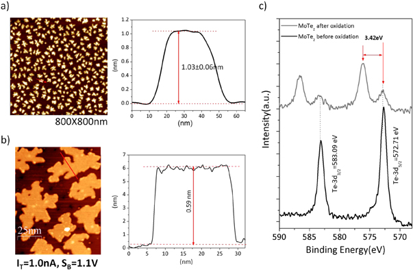
Figure 5. Oxidation of MoTe2 islands by air exposure. (a) Ambient AFM image of MoTe2 monolayer flakes exposed to air. The islands exhibit an island height of ∼1 nm. This is compared to the island height measured for the as grown films by STM of ∼0.6 nm, shown in (b). Te-3d core-level spectroscopy before and after of air exposure is shown in (c). The observed peak shift corresponds to formation of TeO2.
Download figure:
Standard image High-resolution image4. Discussion
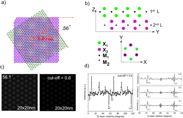
Epitaxial growth of α-MoTe2 on MoS2 has been achieved at 200 °C in a tellurium rich environment. Lower residence time of tellurium compared to Mo is suggested to be responsible for the formation of sub-stoichiometric films with higher annealing temperature and/or reduced tellurium flux. The stoichiometric α-MoTe2 monolayer on MoS2 substrate exhibits a moiré structure with a periodicity of 2.6 ± 0.1 nm. Using the lattice constants for MoS2 and MoTe2 of 0.316 nm and 0.352 nm, respectively, one obtains this moiré periodicity by rotating the two lattices by 56°, as shown in figure 6(a). Note that for a 2H-stacking alternating layers are rotated by 60° thus a 56° corresponds to a 4° rotation with respect to a 2H-stacking sequence. Only one moiré structure is observed in STM studies and under the relatively high annealing temperatures it is reasonable to assume that this rotation represents the lowest energy configuration of this system. Like for single TDCs, the 2H-stacking is the energetically preferred stacking also for TDCs heterostructures [3]. Because of the lattice mismatch between the two layers it is, however, not possible to have this stacking configuration throughout the monolayer. For a related system of a bilayer of WS2/MoS2 the adsorption energies was calculated (by artificially matching the lattice constants) for the favored 2H-structure and compared to the structure with the chalcogen atoms in adjacent layers on-top of each other, rather than in the three-fold hollow sites of the 2H-structure (see figure 6(b) for configuration). For this system an energy difference of 0.0744 eV/cell was calculated. Thus the total energy of a realistic system may be minimized by reducing the number of MoTe2 unit cells for which the Te-atoms are located directly above the sulfur atoms of the MoS2 substrate. We evaluated the fraction of such energetically unfavorable configuration as a function of relative rotation angle between a MoS2 and MoTe2 layer to find the rotation angle that minimizes the configuration with chalcogen atoms of the two layers at the same lateral position. To do this, the two chalcogen-lattices are simulated with cosinusoidal waves, with maxima representing atom positions, using the following expression [13]:
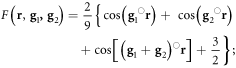
where  and
and  are the primitive reciprocal lattice vector. Forming the product of the two wavefunctions gives a representation of the overlap of the chalcogen atoms in the adjacent layers as shown in figure 6(c). To ignore regions with negligible or no overlap of chalcogen atoms we define a cut-off below which we set all values to 0. Summation of the remaining wavefunction intensity and plotting the variation of this intensity as a function of rotation angle of the two sublattices allows us to determine at which rotation angle the summed intensity is lowest and thus the chalcogen overlap is minimal. Such a plot is shown in figure 6(d). A minimum is observed for a rotation angle of 56.1° or 63.8°, which is within our experimental value for the rotation between MoTe2 and MoS2. This minimum is quite stable for a reasonable range of cut-off values between 0.1 and 0.8. Thus the simple argument of minimizing the number of chalcogen atoms that are directly on top of each other in adjacent layers may give a simple estimation of the rotational angle between transition metal dichalcogen heterostructures in thermodynamic equilibrium. It has to be noted though that this is a very simplistic view and more detailed simulations of the adsorption energies of different moiré structures should be applied, despite the challenges involved in dealing with such large unit-cells.
Figure 6. Moiré pattern and chalcogen-atom overlap as a function of layer-rotation angle. (a) MoTe2/MoS2 bilayer with 56° rotation generates a moiré pattern with 2.6 nm periodicity. (b) Illustration of the energetically preferred 2H-structure for TMDs in side-view and top-view. In the 2H-structure the chalcogen atoms of one layer occupies the three-fold hollow site of the adjacent layer. Also note that for obtaining a 2H-structure the two layers may be considered as rotated by 60° relative to each other, so that the 56° shown in (a) is equivalent to a 4° with respect to a preferred 2H-stacking. Simulation of the overlap of the triangular chalcogen sublattices is shown in (c). The triangualr lattices simulated by wavefunctions and then their product for different rotation angles is plotted on the left in (c). Subsequently a cut-off of 0.6 (see text) is applied on the right in (c). The summation of the waveamplitudes after application of the cut-off condition is shown in (d). Minima in this summation indicate less overlap of chalcogen atoms in adjacent layers and thus potentially energetically more favorable adsorption. The obtained minima at 56° and 64° correspond well to the experimentally observed moire structure for MoTe2/MoS2. The results for the minima does not change significantly by the choice of the cut-off value within a range of 0.1 to 0.8 as is shown on the right of (d).
Download figure:
Standard image High-resolution image
Annealing of α-MoTe2 islands above 500 °C causes a phase transformation that originates at the island edges. This temperature is close to the recently reported phase transition temperature for slightly Te-deficient bulk α-MoTe2 to β-MoTe2 [24]. Thus the observed transition at the edges of α-MoTe2 to β-MoTe2 is likely related to this phase transition. With further annealing, the film becomes strongly tellurium deficient and a MoTe2−x phase is formed. This phase exhibits a strongly anisotropic structure consisting of short one-dimensional strands separated by holes in the layer. This structure is closely related to the structure that forms directly under low tellurium growth conditions and that results in long meandering strands. Since the high temperature β-MoTe2 phase consists of one-dimensional Mo-zigzag chains we speculate that this structure may form the basic unit of these observed strands. However, unlike a contiguous β-MoTe2 plane, we are observing only a few Mo-zigzag chains with tellurium-deficient edges. Regardless of the precise structure, the observation that long one-dimensional MoTe2−x structures can be grown directly on a weakly interacting substrate like MoS2 may make this an interesting structure for further investigation of quasi 1D materials. Although our studies have shown that the direct thermal transformation of monolayer semiconducting α-MoTe2 into semimetallic β-MoTe2 is possible, however, additional loss of Te at high annealing temperature in vacuum results in MoTe2−x phase, which still exhibits an almost metallic (very small band gap semiconductor) electronic structure and also maintains a planar morphology on MoS2. Thus even this tellurium deficient structure may still be used as a planar electrical contact to α -MoTe2 monolayers. For stabilizing β-MoTe2 our studies suggest that it is important to avoid loss of tellurium, which one may achieve by annealing in a sealed, tellurium rich environment.
Finally, the sub-monolayer films we have grown are not stable in air. Generally monolayer materials are more reactive than bulk materials. In our case a high density of step edges, metallic edges, and possibly other defects increases the reactivity [33]. Layer-by-layer oxidation of the surface of bulk TMDs has been reported previously using activated oxygen [34]. Simulations also showed for MoS2 that oxidation is thermodynamically favored but kinetically limited which explains the air stability of MoS2 and shows the important role defects play in the oxidation [35]. The surface oxidation of bulk TMDs or the oxidation of more reactive monolayers at the surface of a TMDs as shown here enables the formation of a conformal oxide layer. This oxide layer may be used subsequently as a seed for growth of an oxide-dielectric by, for example, atomic layer deposition [36]. Thus monolayer growth of a (defective) TMD on a less reactive TMD substrate or other layered materials like grapheme [37], is a potential approach for the growth of conformal oxide dielectrics, which are otherwise difficult to achieve.
5. Summary
Submonolayer growth of MoTe2 on bulk MoS2 substrates by MBE has been investigated by scanning tunneling microscopy and photoemission spectroscopy. For growth of α-MoTe2 tellurium rich conditions and low growth temperatures are needed. However, the formation of minority β-MoTe2 domains could not be avoided. The complete transformation of submonolayer α-MoTe2 into β-MoTe2 by vacuum annealing is prevented by tellurium desorption and formation of tellurium-deficient MoTe2−x. The new tellurium-deficient MoTe2−x forms elongated, quasi-1D structures, which may bear some resemblance to single strands of the anisotropic β-MoTe2 phase. The grown α-MoTe2 monolayer is rotated by ∼56° with respect to the MoS2 substrate resulting in a moiré pattern with 2.6 nm periodicity. Finally the grown MoTe2 layers are not air stable and readily oxidize to MoO3 and TeO2. The resulting oxide layer maintains, however, its two dimensional morphology and thus may be used as a seed layer for subsequent growth of oxide dielectric thin films.
Acknowledgments
Financial support from the National Science Foundation (DMR-1204924) is acknowledged.