
Abstract
The surface chemistry of MoS2, WSe2 and MoSe2 upon ultraviolet (UV)–O3 exposure was studied in situ by x-ray photoelectron spectroscopy (XPS). Differences in reactivity of these transition metal dichalcogenides (TMDs) towards oxidation during UV–O3 were observed and correlated with density functional theory calculations. Also, sequential HfO2 depositions were performed by atomic layer deposition (ALD) while the interfacial reactions were monitored by XPS. It is found that the surface oxides generated on MoSe2 and WSe2 during UV–O3 exposure were reduced by the ALD process ('self-cleaning effect'). The effectiveness of the oxide reduction on these TMDs is discussed and correlated with the HfO2 film uniformity.
Export citation and abstract BibTeX RIS

Content from this work may be used under the terms of the Creative Commons Attribution 3.0 licence. Any further distribution of this work must maintain attribution to the author(s) and the title of the work, journal citation and DOI.
Introduction
Two-dimensional transition metal dichalcogenides (TMDs), as part of the mono- and few-layer materials library, have potentially exceptional properties such as dangling bond-free surfaces and thickness-tunable band gap energies [1, 2], making them outstanding candidates as channel materials for beyond Si-CMOS device structures [3]. The electronic and optoelectronic properties of MoS2, a readily available material in nature, have been extensively studied in recent years [4]. However, the presence of a Schottky barrier at the metal/MoS2 interface has limited the MoS2-based field-effect transistors (FETs) performance [5]. Moving forward into the exploration of other members in the TMD library, several efforts have focused on studying 2D WSe2, where field-effect mobility (μFE) values up to ∼500 cm2 V−1 s−1 have been reported [6]. Furthermore, band–band tunneling properties of WSe2 for tunnel FET applications have been demonstrated [7]. Following these efforts, MoSe2 has been implemented in FETs, exhibiting a promising performance (i.e. μFE ∼ 150–200 eV) according to recent reports [8, 9]. It has been demonstrated theoretically [10] and experimentally [11–13] that the limiting effect on mobility associated with Coulomb scattering can be reduced by a having a dielectric material on the 2D channel, motivating several studies related to dielectrics on TMDs. However, it has also been shown that, given the relative inertness of the TMDs surfaces, the direct atomic layer deposition (ALD) of high-k dielectrics on clean, un-treated surfaces results in the formation of clusters or islands instead of continuous films[14, 15]. Previously, it was shown that uniform, pin-hole free and thin (∼4 nm) Al2O3 films can be obtained by performing a ultraviolet (UV)–O3 surface pre-treatment on MoS2, where covalent oxygen functionalization of the MoS2 top-most sulfur layer occurred, while avoiding molybdenum oxidation [16]. Alternative processes have been reported in order to improve the ALD high-k nucleation on MoS2 such as oxygen plasma pre-treatment [15], the use of ozone as an oxidant precursor during ALD of Al2O3 [17], and metal-oxide seed layers [18].
Yet, whether the proposed processes can be directly extended to other TMDs remains an important question, since different compositions could result in variation of surface properties. Here, in situ monochromatic x-ray photoelectron spectroscopy (XPS) studies were used to characterize the effect of a UV–ozone treatment of MoSe2 and WSe2 single crystal surfaces. Also, the surface reactivity towards oxidation of these TMDs was compared and modeled by density functional theory (DFT) calculations. It was found that surface oxides formed upon UV–O3 exposure of the diselenides surface. Additionally, XPS monitored the interfacial chemistry between ALD-HfO2 and the UV–O3 treated TMD surfaces. Finally, the HfO2 film uniformity on the UV–O3 treated TMDs was investigated and correlated with the interfacial chemistry.
Experimental details
The UV–O3 treatments and ALD studies described here were performed in situ using an ultrahigh vacuum (UHV) cluster tool described elsewhere [19]. XPS was carried out using a monochromated Al K x-ray source (hν = 1486.7 eV) and equipped with a seven channel analyzer, using a 15 eV pass energy. The XPS peak deconvolution was achieved with the software Aanalyzer® [20], using Voigt functions with independent control of the Lorentzian and Gaussian components, and applying a dynamic Shirley background subtraction. The top-most layers from MoS2 (SPI Supplies), MoSe2 (2D Materials) and WSe2 (Nanoscience Instruments) bulk crystals (all (0001) orientation) were mechanically exfoliated using Scotch® Magic™ tape, and the freshly as-exfoliated bulk materials were loaded immediately into UHV. All the UV–O3 exposures were performed at room temperature as described in [16]. In an interconnected chamber, the sample surfaces are placed within a few mm from a UV lamp (low pressure mercury lamp) in the presence of O2 (O2 partial pressure
  to generate ozone [21]. The ALD experiments were performed using a Picosun ALD reactor, with an operating pressure of ∼10 mbar. The hot wall reactor is integrated to the cluster tool to enable surface analysis without spurious contamination from atmospheric exposure [19]. For the HfO2 deposition, tetrakis (dimethylamino) hafnium (TDMA-Hf) and H2O were used as the precursors, having a substrate deposition temperature of 200 °C. The precursor pulse and purge times are 0.1 and 4 s, respectively. High purity (99.999%) N2 was used as the precursor carrier and purging gas. After one full-cycle of TDMA-Hf and H2O, the samples were taken out from the ALD reactor and transported to the XPS analysis chamber through a transfer tube under UHV (∼1 × 10⁻¹⁰ mbar). After analysis, the samples were transported back to the ALD reactor for further deposition. This process was repeated for subsequent depositions for a total of 30 ALD cycles. Tapping-mode atomic force microscopy (AFM) images were obtained ex situ using an atomic probe microscope Veeco, Model 3100 Dimension V. High angle annular dark field scanning transmission electron microscopy (STEM) was performed using a JEOL ARM200F with probe spherical aberration (Cs) corrected operated at 200 kV. TEM sample preparation was accomplished using a FIB-SEM Nova 200.
The first-principles modeling, based on DFT [22, 23] with plane wave basis sets and Projector Augmented Wave pseudopotentials [23, 24] as implemented in the Vienna ab initio Simulation Package [22, 25, 26] were conducted to find the energetics of oxidation. The electronic wave functions were represented by plane wave basis with a cutoff energy of 500 eV. The exchange and correlation interactions were incorporated as a functional of the generalized gradient approximation [24, 27, 28]. A 5 × 5 supercell of host MX2 monolayers (M = W or Mo and X = S, Se) was used for the DFT calculations. Each model has ∼16 Å vacuum to avoid interaction between replica images as a result of the periodic boundary conditions. The k point grid of 12 × 12 × 1 was adopted for Brillouin zone sampling. The energy and Hellmann-Feynman force convergence criteria chosen were 10−4 eV and 0.01 eV Å−1, respectively.
Results and discussion
In order to determine whether oxygen functionalization by UV–O3 was extendable to TMDs beyond MoS2, a room temperature UV–O3 treatment was performed on WSe2 and MoSe2, while MoS2 was also used as a control sample for comparison with previous work [16]. XPS spectra of MoS2, MoSe2, and WSe2, after 3, 6 and 15 min of UV–O3 exposure, is shown in figures 1(a)–(c) respectively, while table 1 summarizes the bonds formed after UV–O3, showing their binding energy (BE) and ratios of the integrated intensity of the corresponding peaks with respect to the bulk signal. The sequential UV–O3 exposure on MoS2 shows that S–O bond formation is detected after 3 min, and by increasing the exposure time, i.e. 6 and 15 min, the oxygen adsorption saturates to form 1 ML [16]. Under these conditions, no Mo–O bond formation is detected, as previously reported. It has also been reported that UV–O3 can cause molybdenum oxidation in MoS2, when the exposure is much longer (60 min) [29]. This implies that the oxidation process is dose and time dependent.

Figure 1. XPS spectra of the initial as-exfoliated surface and after 3 min, 6 min and 15 min of UV–O3 exposure for (a) MoS2 (Mo 3d, S 2p), (b) MoSe2 (Mo 3d, Se 3d) and (c) WSe2 (Se 3d, W 4f). Optimized (d) MoS2, (e) MoSe2 and (f) WSe2 structures after oxygen adsorption on top of the chalcogen atom (top view) and after replacement of the chalcogen atom with an oxygen atom (tilted top view).
Download figure:
Standard image High-resolution imageTable 1. Chemical species detected on MoSe2, WSe2 and MoS2 after different UV–O3 exposure times, showing the corresponding peak positions in eV and their integrated intensity ratio with respect to the bulk peak (shown in brackets'[]').
| UV–O3 treatment time | 3 min | 6 min | 15 min | |||
|---|---|---|---|---|---|---|
| S 2p | S–O 162.9 [0.06] | S–O 162.9 [0.1] | S–O 162.9 [0.1] | |||
| MoS2 | Mo 3d | — | — | — | ||
| Se 3d | Se–O 56.3 [0.04] | MoSexOy 55.4 [0.05] | SeOx 59.1 [0.10] | MoSexOy 55.4 [0.12) | SeOx 59.5 [0.34] | |
| MoSe2 | Mo 3d | — | MoSexOy 229.8 [0.05] | MoOx 233.0 [0.22] | MoSexOy 229.7 [0.10] | MoOx 233.4 [0.79] |
| Se 3d | Se–O 56.5 [0.02] | Se–O 56.5 [0.02] | SeOx 59.3 [0.14] | WSexOy 55.4 [0.07] | SeOx 59.6 [0.22] | |
| WSe2 | W4f | — | WOx 36.1 [0.18] | WSexOy 33.1 [0.06] | WOx 36.3 [0.45] | |
In the case of MoSe2, the 3 min UV–O3 exposure initially results in the formation of Se–O bonding, without causing Mo oxidation. The nature of the Se–O results analogous to the S–O observed in MoS2 [16], which may be described as chemisorbed oxygen on the surface, i.e. covalent bond formation between oxygen and the top most selenium layer, while preserving the covalent bonding within the MoSe2 layer. However, in contrast to MoS2, the 6 min UV–ozone exposure results in sub-stoichiometric molybdenum oxide (MoOx) formation. The MoOx peak shows a symmetric lineshape, suggesting that Mo is present in only one of the seven different phases that has been identified for MoOx, x = 2.75–3 [30, 31]. In the Se 3d region, the previously observed Se–O bond is below the detection limit, however, a new peak at ∼59 eV indicates that selenium is further oxidized forming a selenium sub-oxide SeOx. In addition, an extra feature at ∼0.6 eV higher in binding energy than the bulk MoSe2 peak is observed in both Mo 3d and Se 3d core levels (blue peak in figure 1(b)).
Previous studies in MoS2 correlated the appearance of peaks at higher BE from the main bulk peak, for both Mo 3d and S 2p, with the existence of molybdenum oxysulphide (MoSxOy) [32–34], where the BE position of such peaks was dependent on the x and y values. A peak at a slightly higher BE (∼0.5–0.8 eV) than the characteristic MoSe2 peak in Se 3d could be also correlated with metallic Se [35], however, the fact that both core levels showed this high BE feature makes this chemical state assignment less probable. Another possible assignment could be a sub-stoichiometric MoSex phase, however, the existence of MoSex would cause the transition metal peak to shift lower in BE and the chalcogen peak to broaden [36], and this situation is not observed. Thus, the feature in blue in figure 1(b) is associated with MoSexOy formation, caused by oxidation during UV–O3 exposure. Finally, after UV–O3 for 15 min, the MoOx peak shifted to 0.4 eV higher BE which is consistent with a higher oxygen content in MoOx [30, 37]. Also, the MoOx oxide to bulk peak intensity ratio increases in comparison to the 6 min ratio, showing that the oxygen is inserted deeper within the material. In the case of Se 3d, the sub-stoichiometric SeOx shows a shift to 0.4 eV higher BE, suggesting complete oxidation to SeO2.
In comparison, figure 1(c) shows the XPS spectra of WSe2 for the same UV–O3 exposure times. After UV–O3 exposure for 3 and 6 min, Se–O bonding is detected however the Se–O to bulk WSe2 peak intensity ratio is lower than that for MoSe2. W oxidation in the form of WOx is detected after 6 min of exposure. Similar to MoSe2, the UV–O3 exposure of WSe2 presents tungsten oxyselenide bonding (WSexOy) after 15 min of exposure, in addition to WOx and SeOx formation.
Oxidation studies of these TMDs in the bulk form were performed previously by Jaegermann, et al [38], where reactivity towards oxidation was found to go from lower to higher in the sequence: MoS2 < MoSe2 < WSe2. This tendency was related to the degree of mixed metal d-states from the transition metal with the p-states in the chalcogenide, based on ionization energies arguments. However, the focus of that study was the photoelectrochemical oxidation in solution, using electrolytes (i.e. K2SO4) as oxidizers, which might introduce additional variables in the oxidation processes. Thus, DFT calculations were performed in order to have a better understanding of the energetics involved in the oxidation of TMDs.
Figures 1(d)–(f) shows optimized structures for MoS2, MoSe2 and WSe2, respectively, when an oxygen atom is adsorbed on top of the chalcogen (O–Se, O–S) and when oxygen substituted the chalcogen to form a transition metal–oxygen bond (O–Mo, O–W). The calculated formation energies of the oxygen adsorption and chalcogen substitution with oxygen are listed in table 2, which were obtained using the following equation:

where Eform is the formation energy of the adsorbed or substitutional oxygen on MX2 surfaces with total DFT energy E (O:MX2), E (pristine) is the DFT energy of the pristine MX2 surfaces ((M = W or Mo and X = S, Se), μO and μS are the reference chemical potentials of O (oxygen molecule) and S (bulk sulfur) and n is the number of adsorption or substitutional O atoms. Under this definition, negative values of the formation energy refer to thermodynamically stable oxidation process.
Table 2.
Formation energies of oxygen adsorption ( and oxygen replacement (
 on MoSe2 and WSe2 calculated by DFT.
 (eV) (eV) |
 (eV) (eV) |
|
|---|---|---|
| O–S | O–Mo | |
| MoS2 | −1.12 | −1.912 |
| O–Se | O–Mo | |
| MoSe2 | −0.284 | −2.504 |
| O–Se | O–W | |
| WSe2 | −0.132 | −2.814 |
According to the formation energies shown in table 2, O–S bond formation in MoS2 is more energetically favorable and therefore more stable in comparison to O–Se in MoSe2 and WSe2. The DFT calculations also indicate that oxygen desorption will occur more easily in MoSe2 and WSe2, in comparison to MoS2. The formation energy required for the replacement of the chalcogen to form a direct bond between oxygen and the transition metal is found to be more energetically favorable in the case of MoSe2 and WSe2 than for MoS2, which is consistent with the XPS results after UV–O3 exposure. The relative lower stability of the O–Se bond in comparison to O–S implies that desorption of oxygen, and possibly the 'kick-out' [39] of O–Se species, can leave unsaturated bonds for the transition metal, which then are readily available to form Mo–O and W–O bonds in presence of oxygen, such as during a UV–O3 exposure. Experimentally, this oxidation process caused the formation surface oxides of 0.36 nm and 1 nm thickness in MoSe2 for 6 min and 15 min of UV–O3 exposure respectively, while the surface oxides in WSe2 exhibited 0.33 nm and 0.66 nm thicknesses for the same mentioned exposure times, according with XPS thickness calculations.
These UV–O3 exposure studies demonstrate that oxygen functionalization of MoSe2 and WSe2 surfaces is more difficult to control compared to MoS2. Yet, the impact of having surface oxides on these TMDs prior to high-κ dielectric deposition by ALD is still of interest. Thus, HfO2 was sequentially deposited by ALD on the UV–O3 treated MoSe2 and WSe2, while the interface chemistry was monitored by XPS. For comparison purposes, all the samples discussed here received a UV–O3 exposure for 6 min.
Figure 2(a) shows that after one ALD cycle on functionalized MoSe2, the MoOx peak intensity significantly decreases to ∼24% its initial intensity. In the Mo 3d region, a new peak is detected at 231.9 eV, which is designated as the Mo5+ oxidation state [40], indicating that the Mo–O bonds are reduced (i.e. O was transferred to Hf, resulting a lower oxidation state of Mo). Additionally, the SeOx intensity decreases to below the detection limit, as shown in the Se 3d region. The decrease in oxide intensity during precursor pulsing in ALD, or 'self-cleaning', effect was previously studied for III–V materials, such as InxGa1−x As [41]. The self-cleaning reduction reactions that occurred after one cycle result in the gradual reduction of the oxidation state from Mo6+ to Mo5+. In addition, the fact that no Mo0 or other chemical state was detected suggests that MoOx went through a ligand exchange reaction with the Hf precursor, forming a volatile molybdenum compound possibly of the form Mo(N(CH3)2)x [42]. Based on the thermodynamic quantities, HfO2, with a Gibbs free-energy of formation of −251.8 kcal mol−1 [43], results in a more energetically favorable reaction product than MoOx, assuming that the Gibbs free-energy of MoOx is close to—159.65 kcal mol−1 [44], which is the corresponding value for MoO3.

Figure 2. (a) XPS spectra showing the evolution of the Mo 3d, Se 3d and (c) Hf 4f core level from the UV–O3 treated MoSe2 after sequential HfO2 deposition by ALD (b) The MoOx (SeOx) to MoSe2 peak ratio, obtained from their respective integrated intensities. The inset in (c) shows the Hf 4f integrated intensity with respect to the number of ALD cycles.
Download figure:
Standard image High-resolution imageFor the Se 3d feature, no lower oxidation states are detected (i.e. S0), indicating that SeOx, a volatile compound, may be thermally desorbed from the surface in vapor phase [45]. Finally, the MoSexOy peak is not observed after one cycle, suggesting that the MoSexOy phase possibly recovers its initial state as MoSe2 through the SeOx desorption channel, thus contributing to the bulk Se peak signal intensity.
Further deposition of HfO2 using five ALD cycles results in a decrease of the Mo6+ intensity to below the detection limit; only Mo5+ remains. As shown in figure 2(b), the Mo5+ to MoSe2 integrated intensity ratio is ∼0.03, suggesting that most of the surface oxides undergo 'self-cleaning' reactions. The Se 3d spectra show no change after five cycles. After ten cycles, no interfacial oxides from MoSe2 are detected, and further HfO2 deposition only caused attenuation of the MoSe2 features. Figure 3(c) shows that the chemical identity of HfO2 remains constant through the sequential depositions.

Figure 3. (a) XPS spectra showing the evolution of the W 3d, Se 3d, and (c) Hf 4f core level from the UV–O3 treated WSe2 after sequential HfO2 deposition by ALD. (b) The WOx (SeOx) to WSe2 peak ratio, obtained from their respective integrated intensities. (c) Hf 4f spectra after 1, 5, 10 and 30 ALD cycles on UV–O3 treated WSe2. The inset in (c) shows the Hf 4f integrated intensity with respect to the number of ALD cycles.
Download figure:
Standard image High-resolution imageIn an analogous process, HfO2 was sequentially deposited on UV–O3 treated WSe2 followed by XPS analysis. Figure 3(a) shows the evolution of WSe2 chemical states through the experiment. It is shown that, in contrast to MoSe2, the decrease in intensity of the transition metal oxide in WSe2 is minimal after the first cycle. In fact, the WOx to bulk intensity ratio remains constant, however the Se–O intensity decreases below the detection limit, and the SeOx to WSe2 ratio decreases by ∼44%. Also, the HfO2 signal intensity after the first cycle of deposition on WSe2 (figure 3(c)) is smaller in comparison to that obtained for MoSe2 (figure 3(c)).
Even when the formation of HfO2 is more energetically favorable than WOx based on the Gibbs free energy (WO3 ≈ −195.7 kcal mol−1) [44], WOx remains on the WSe2 surface, exhibiting lower reactivity during the ALD 'self-cleaning' reduction reactions in comparison to MoOx. Various hypotheses can be made to explain the limited HfO2 growth. First, assuming a ligand exchange mechanism as in the case of MoSe2, then dissociation of W–O bond would be needed. The dissociation energy of the W–O bond is 720 ± 71 kJ mol−1 [46], which is much higher than the Mo–O dissociation energy 597.2 ± 33.5 kJ mol−1 [46] thus the oxygen loss in WOx and subsequent formation of a volatile W(N(CH3)x) compound requires a higher energy than MoOx. Secondly, WO3 and MoO3 clusters are well known for their catalytic properties toward oxidation, where it was found that Mo6+ will be more easily reduced to Mo5+ than W6+ to W5+ due to the high stability of WO3 [47]. This is consistent with our observation in MoOx and WOx reactivity after one ALD cycle. The capability of WOx to remain in the W6+ oxidation state makes WOx an effective oxidizing agent of organic molecules [34]. Thus, another possible scenario is the reaction between WOx and the organic ligand in TDMA-Hf inhibiting ligand exchange reactions. In fact, from the C1s spectra, which overlap with a Se Auger feature, additional carbon species are detected in WSe2 in comparison to MoSe2 after the first cycle and subsequent cycles (see supplementary information (SI)).
After five cycles, the WOx to WSe2 peak ratio decreases by only 5% along with a WOx peak shift to a lower BE of ∼0.2 eV, while the SOx to WSe2 peak ratio decreases by 31% from its previous value. Interestingly, extra features at identical lower BE positions from the bulk WSe2 signals, for both W 4f and Se 3d are detected. The appearance of low BE peaks in WSe2 was previously reported and attributed to a non-van der Waals surface, [48] characterized by edge planes and stepped surfaces. Such a non-homogeneous surface potential can give raise to different fermi level positioning, shifting the core levels in WSe2 the same amount. Thus, these newly identified peaks can be identified as WSe2 with a different fermi level in reference to the initial WSe2. A non-van der Waals surface could be generated from desorption of surface oxides leaving regions in WSe2 with unsaturated bonds and/or partially etched areas. After 30 ALD cycles, the SeOx is below the detection limit, and the WOx to WSe2 peak intensity ratio decreases to a value of 0.08, with a final BE position ∼0.53 eV lower than the initial WOx BE, due to lower oxygen content in WOx [49]. This indicates that lower oxygen content in WO x improves the rate of ligand exchange reactions between WOx and TDMA-Hf.
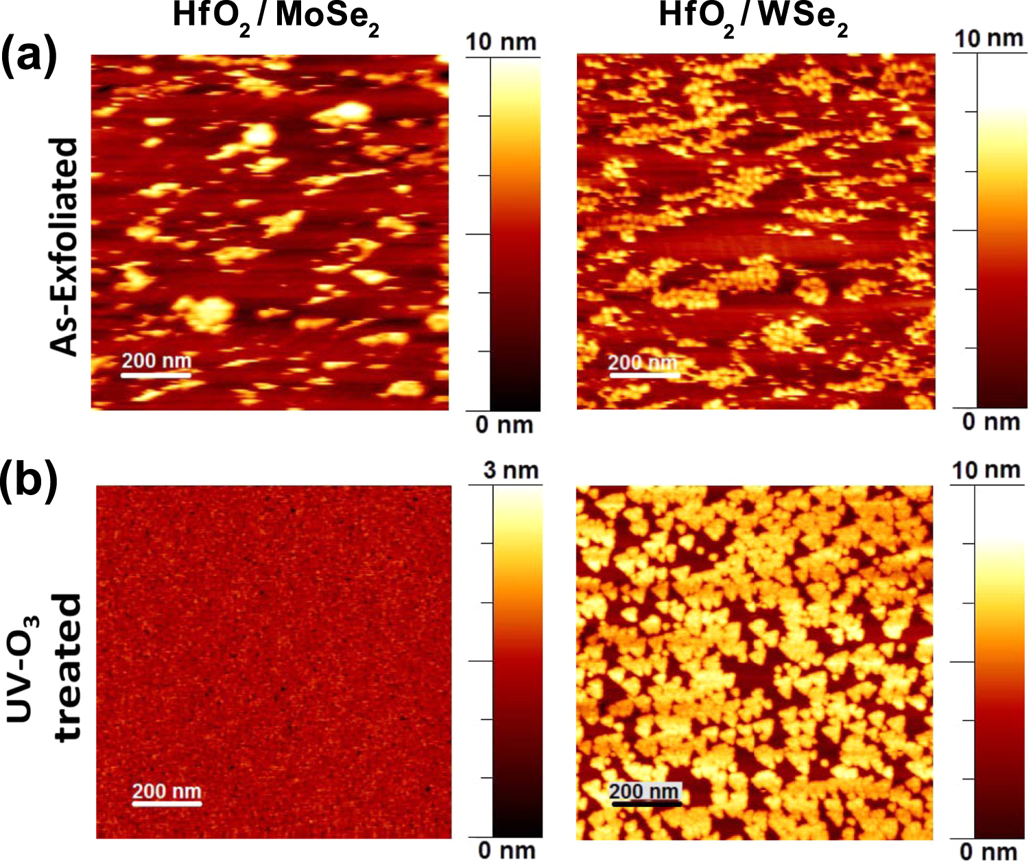
It should be noted that the Hf 4f integrated intensity is significantly different on MoSe2 and WSe2 for same number of cycles by comparing figures 2(c) and 3(c), where the final HfO2 content on MoSe2 is about three times that detected on WSe2, suggesting differences in HfO2 coverage. For such reasons, the surface topography of the HfO2 films on the UV–O3 exposed TMDs was also investigated by ex situ AFM. For comparison, HfO2 was deposited (30 cycles of TDMA-Hf and H2O) on as-exfoliated non-treated samples, where the dearth of reactive sites on the MoSe2 and WSe2 surfaces impeded uniform ALD nucleation, thus HfO2 is deposited following an island-type growth mechanism, as observed on MoS2 [14]. In contrast, on the UV–O3 treated MoSe2, the HfO2 film is fully covered and pin-hole free (figure 4(a)). Therefore, the presence of surface oxides formed after UV–O3 enhanced HfO2 growth rate in comparison to non-treated MoSe2, leaving as a result a completely covered HfO2 film with a RMS roughness of only 0.15 nm. Interestingly, on the UV–O3 treated WSe2, HfO2 islands with a triangular shape are formed with edge length and height in the range of 30–60 nm and 4–5 nm, respectively. It has been shown that triangular hole-like structures can be generated on WSe2 by oxidative electrochemical etching promoted by AFM [50, 51] and STM [52, 53] tip-sample voltage. In this case, the presence of triangular hole-like structures on WSe2 could have served as nucleation site for HfO2, resulting in a quasi-ordered triangular cluster growth. This implies that oxidative etching of WSe2 could have taken place during UV–O3 exposure for 6 min and/or ALD self-cleaning reactions. In fact, the last hypothesis correlates with the newly detected WSe2 XPS peaks (blue features in figure 3(a)) and in turn with the formation of a non-van der Waals surface, as discussed previously.

Figure 4. 1 × 1 μm2 AFM images of HfO2 on (a) as-exfoliated and (b) UV–O3 treated MoSe2 and WSe2.
Download figure:
Standard image High-resolution imageIn accordance with the AFM results, cross-section STEM images in figure 5(a) shows a uniform HfO2 film with thickness of ∼4 nm on UV–O3 treated MoSe2, having a minimal variation in thickness across a length of 0.25 μm (see SI). Interestingly, the top-most MoSe2 surface exhibits darker contrast regions that correspond to selenium-deficient MoSe2 according to electron energy loss spectroscopy line scans across the HfO2–MoSe2 interface (shown in the SI). The ALD self-cleaning reactions occurred right at the MoSe2 surface are likely to be involved in the generation of such selenium-deficient regions. It is also evident that the MoSe2 layers below the darker contrast region are continuous and unaltered.

Figure 5. STEM micrographs corresponding to (a) HfO2 on UV–O3 treated MoSe2 and (b) HfO2 on UV–O3 treated WSe2 interfaces. 1L = One layer.
Download figure:
Standard image High-resolution image
Finally, the high magnification STEM image in figure 5(b) gives further insights in regard to HfO2 on the UV–O3 treated WSe2. Partially etched WSe2 layers are identified at the interface with the HfO2 islands, which correlates with the XPS and AFM results described above. Here, the contrast from the partially etched WSe2 layers is weaker at the HfO2/WSe2 interface than it is in the bulk WSe2. This can be explained by considering that an STEM image is averaging cross-sectional information from a finite ∼100 nm thick material. Since the triangular hole-like structures observed in this work have an area smaller than the thickness analyzed in cross-section by STEM, their presence could only be observed in STEM as a weakening of the contrast, while some signal from the un-etched portions of that same layer will always be obtained. Clearly, various mechanisms are involved in the HfO2 growth on UV–O3 treated WSe2. First, the presence of WOx on the WSe2 surface and its relative high stability during self-cleaning reactions slows down the HfO2 growth rate in comparison to MoSe2 for same number of cycles, generating a partially covered HfO2 film. Secondly, the presence of triangular hole-like structures on WSe2 generated by etching caused the preferential HfO2 nucleation on such structures, forming triangular HfO2 islands.
Conclusions
In summary, it is found that selective oxygen functionalization of the selenium-based TMDs studied here is limited by highly energetically favorable oxidation of the transition metal. These results highlight the importance that the TMD composition has on the reactivity towards oxidation. The investigation of the ALD of HfO2 on the TMDs with initial surface oxides elucidates self-cleaning reduction reactions and the desorption of volatile species during the ALD process. According to the interface study, the surface oxides on MoSe2 are completely removed by the self-cleaning reduction reaction upon HfO2 deposition. In contrast, the self-cleaning effect is less effective in the oxide removal on WSe2 mainly due to the relative stability that WOx exhibits. Thus, the ability of assisting the HfO2 nucleation is superior for MoOx than WOx. Finally, the coverage of HfO2 on the TMD surfaces was improved by the UV–O3 pre-treatment.
Acknowledgments
This work is supported in part by the Center for Low Energy Systems Technology (LEAST), one of six centers supported by the STARnet phase of the Focus Center Research Program (FCRP), a Semiconductor Research Corporation program sponsored by MARCO and DARPA. It is also supported by the SWAN Center, a SRC center sponsored by the Nanoelectronics Research Initiative and NIST. All the DFT calculations are performed using the computational resources of Texas Advanced Computer Center (TACC) at the University of Texas at Austin.