
Abstract
The deterministic transfer of two-dimensional crystals constitutes a crucial step towards the fabrication of heterostructures based on the artificial stacking of two-dimensional materials. Moreover, controlling the positioning of two-dimensional crystals facilitates their integration in complex devices, which enables the exploration of novel applications and the discovery of new phenomena in these materials. To date, deterministic transfer methods rely on the use of sacrificial polymer layers and wet chemistry to some extent. Here, we develop an all-dry transfer method that relies on viscoelastic stamps and does not employ any wet chemistry step. This is found to be very advantageous to freely suspend these materials as there are no capillary forces involved in the process. Moreover, the whole fabrication process is quick, efficient, clean and it can be performed with high yield.
Export citation and abstract BibTeX RIS
Since its isolation in 2004 [1], graphene has created huge interest in the scientific community [2]. This breakthrough also constitutes the origin of a new research topic devoted to the study of two-dimensional atomic crystals [3]. One of the key breakthroughs in the success of graphene research was the development of the micromechanical exfoliation method (the so-called Scotch tape method). Despite the simplicity of this method it can provide extremely high quality samples [4]. Nevertheless, the exfoliation method produces flakes with different sizes and thicknesses randomly distributed over the sample substrate, and only a small fraction of these flakes are atomically thin. The introduction of the optical identification method to find atomically thin crystals from the crowd of thicker bulky flakes constitutes the second key breakthrough to guarantee the success of graphene-related research as it provides a fast, reliable and non-destructive way of locating the flakes [5–7]. The combination of mechanical exfoliation and optical identification, however, cannot provide a reliable way to fabricate more complex systems such as heterostructures formed by artificially stacking different 2D crystals [8–14]. The probability of creating these heterostructures by randomly depositing different 2D crystals onto the substrate is too small. To fabricate such systems new experimental approaches are needed to place the 2D crystals at a specific location [15, 16]. Three of these deterministic transfer methods are rather extended nowadays: the wedging method [17], the polyvinylalcohol (PVA) method [18] and the evalcite method [19].
In the wedging transfer method water is used to lift off a hydrophobic polymer layer spin-coated onto a hydrophilic substrate. If the hydrophilic substrate is covered by flakes, they can be lifted off with the hydrophobic polymer layer and transferred to another substrate using water as the transfer-active component. After the transfer, the hydrophilic polymer layer has to be removed with solvents. In the PVA transfer method, the flakes are transferred onto a polymer sacrificial layer (spin-coated on a substrate previously treated with a water soluble PVA polymer layer). The substrate is floated on the surface of a deionized water bath and once the water-soluble polymer has dissolved, the substrate sinks to the bottom of the bath and the polymer layer is scooped and subsequently dried. The polymer layer is then mounted in a micromanipulator to transfer the flakes to an arbitrary substrate. After transfer, the polymer sacrificial layer is dissolved with solvents. Finally, in the evalcite method, the flakes are transferred onto a glass slide which has been spin-coated with a low glass temperature polymer (evalcite). The glass slide is mounted in a micromanipulator and the acceptor substrate is heated up to 75–100 °C. When the polymer touches the substrate it melts and adheres strongly to the surface, facilitating the transfer from the glass slide to the surface. After the transfer, the polymer layer has to be removed with solvents as in the previous methods.
All these transfer methods thus rely on sacrificial polymer layers and require a wet process at some stage of the fabrication process. This characteristic may hamper their usability as the acceptor surface may contain structures sensitive to the chemicals employed or to the capillary forces involved in the process. For instance, fabrication of freely suspended structures by conventional wet transfer methods remains challenging as they tend to collapse by the capillary forces. An all-dry alternative transfer method is therefore necessary to widen the range of applications of the deterministic transfer methods and to avoid contamination of the fabricated structures. In this paper we present an all-dry transfer method that relies on viscoelastic stamps. Two-dimensional crystals are transferred with this method without employing any wet chemistry. It is found to be very advantageous to freely suspend these materials as there are no capillary forces involved in the process. Fabrication of artificial heterostructures and freely suspended atomically thin layers and the transfer of 2D crystals onto arbitrary substrates are demonstrated.
The experimental setup employed to transfer two-dimensional crystals comprises an optical microscope (Olympus BX 51 supplemented with an Olympus DP25 digital camera) supplemented with large working distance optical objectives and a three axis micrometer stage to accurately position the stamp (see figure 1(a)), very similar to the setups employed in other transfer methods [17–19]. We have also developed a dedicated setup to carry out the transfer process which shows even better performance than the modified optical microscope with a much lower price (see supporting information for more details of this dedicated transfer setup, available from stacks.iop.org/2DM/1/011002/mmedia).

Figure 1. Deterministic transfer setup and process. (a) Schematic diagram of the experimental setup employed for the all-dry transfer process. (b) Diagram of the steps involved in the preparation of the viscoelastic stamp and the deterministic transfer of an atomically thin flake onto a user-defined location (for instance another atomically thin flake).
Download figure:
Standard image High-resolution imageThe stamp is a thin layer of commercially available viscoelastic material (Gelfilm from Gelpak) which is adhered to a glass slide to facilitate its handling. The two-dimensional crystals to be transferred are deposited onto the viscoelastic layer by mechanical exfoliation of the bulk layered crystal with Nitto tape (figure 1(b)). The surface of the stamp is inspected under the optical microscope to select the thinner flakes due to their faint contrast under normal illumination. As the stamp is transparent, transmission mode can be used to determine the number of layers. Raman spectroscopy can also be carried out on the surface of the stamp to confirm the thickness of the flake [20, 21]. Once a thin flake has been identified, the acceptor substrate is fixed on the sample XYZ stage using double-sided tape. The stamp is then attached to the three axis manipulator with the flakes facing towards the sample. As the stamp is transparent, one can see the sample through it and thus it is possible to align the desired flake on the acceptor surface where one wants to transfer the flake at sub-micrometer resolution. A step-by-step guide of the transfer process can be found in the supporting information, available from stacks.iop.org/2DM/1/011002/mmedia.
In order to transfer the flake to the acceptor surface, the stamp is pressed against the surface and it is peeled off very slowly. The working principle of the transfer is based on the viscoelasticity: the stamp behaves as an elastic solid over short timescales while it can slowly flow over long timescales [22]. Flakes adhere to its surface because the viscoelastic material is in intimate contact with the flakes. By slowly peeling off the stamp from the surface, the viscoelastic material detaches, releasing the flakes that adhere preferentially to the acceptor surface.
The potential of the presented technique is illustrated by transferring a few-layer graphene (FLG) flake onto h-BN. Figure 2(a) shows an example of an FLG flake deposited on the viscoelastic stamp. Figure 2(b) shows the h-BN flake, previously deposited on a Si/SiO2 substrate by mechanical exfoliation (see materials and methods section in the supporting information), as seen through the viscoelastic stamp when the separation between the sample and the stamp is still large. When the stamp is brought closer and closer to the sample, the FLG flake appears more clearly as it gets more and more focused (figure 2(c)). At this stage, it is still possible to align the flake to the h-BN flake using the XY knobs of the stamp stage. Once both flakes are aligned, the stamp is brought into contact with the acceptor surface, which can be clearly seen by a sudden change in color (figure 2(d)). Once in contact, the stamp is not pressed further against the sample and it is peeled off very slowly (figure 2(e)). Figure 2(f) shows the optical image of the transferred FLG flake after removing the stamp. The topography of the transferred flake is shown in figure 2(g), demonstrating that the FLG flake lays flat on the h-BN surface without bubbles or wrinkles. The whole transfer process can be accomplished in less than 15 min (see the supporting information for a real time video of the stamping process, available from stacks.iop.org/2DM/1/011002/mmedia) [23].

Figure 2. Placing a few-layer graphene flake onto a hexagonal boron nitride flake. (a)--(f) Optical micrographs acquired during the transfer process. (a) A few-layer graphene flake has been identified on the surface of the viscoelastic stamp. (b) A boron nitride flake has been selected on the acceptor surface. (c) The few-layer graphene flake is aligned on top of the boron nitride with a three axis micrometer positioner and looking through the transparent stamp during handling. (d) Once the flake is aligned, the stamp is brought into contact with the sample. During this process the few-layer graphene flake becomes more and more focused. (e) The viscoelastic stamp is peeled off very slowly until the few-layer graphene flake is fully transferred. (f) The resulting heterostructure of few-layer graphene onto a boron nitride flake. (g) AFM topography of the transferred FLG flake (acquired on the area highlighted with a dashed square in (f)). A topographic line profile has been included as an inset.
Download figure:
Standard image High-resolution imageThe method can be applied to any kind of exfoliable layered crystals, allowing for almost infinite combinations of materials. We found that, with the dry transfer process, one can achieve a yield close to 100% when transferring onto atomically flat materials (to fabricate heterostructures, for instance). When rougher substrates are employed (such as samples with evaporated metals or with abrupt changes in their topography) the yield can be lower due to the reduced adhesion forces between the 2D material and the substrate. Figure 3 shows some examples of atomically thin heterostructures fabricated by stacking other two-dimensional materials and employing this transfer technique. In figure 3(c), the transfer process has been repeated to fabricate a 'sandwiched' MoS2 bilayer in between two h-BN flakes (see supporting information). Dashed lines have been used to highlight the different materials in the optical microscopy images (cartoons of the fabricated heterostructures are depicted above the optical images). The topography of the samples has been characterized by atomic force microscopy (AFM), which is shown above the each optical microscopy image. Line profiles are included in the AFM images as insets to determine the thickness and the roughness of the transferred flakes. Note that although the fabricated heterostructures have not been subjected to any post-fabrication annealing step, their surfaces are clean of contaminants (typically present on samples fabricated by wet-transfer procedures).

Figure 3. Artificial heterostructures. Optical and AFM images of some heterostructures fabricated by stacking different two-dimensional crystals (h-BN, MoS2 and mica) with our all-dry transfer technique. A sketch of the fabricated heterostructure is shown above the optical images (at the left side). Atomic force microscopy images (acquired in the regions highlighted by a black square in the optical images) are also shown above the optical images (at the right side). (a) Mono- and bilayer MoS2 onto h-BN. (b) Bilayer MoS2 onto a muscovite mica flake. (c) A bilayer MoS2 flake 'sandwiched' between two h-BN flakes.
Download figure:
Standard image High-resolution imageWe found that an excessive pressure applied during the transfer process may deform the viscoelastic stamp material yielding a high density of bubbles after the peeling off stage because of the sudden release of strain, similar to what has been observed in reference [24] (see supporting information). Nonetheless by carefully controlling the transfer pressure one can typically achieve large flat areas (as those shown in figure 3) without wrinkles and bubbles, which is desirable for further fabrication of devices out of these heterostructures. The fabrication of heterostructures with large areas without bubbles and wrinkles can be achieved with yields of 30--40%. Section 9 of the supporting information presents the Raman spectroscopy characterization of some MoS2 flakes transferred onto h-BN flakes. A thorough Raman spectroscopy and photoluminescence characterization of all-dry transferred heterostructures can be found in reference [25].
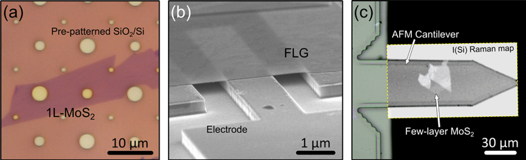
Another advantage of the all-dry transfer technique is that, due to the lack of capillary forces involved during the transfer procedure, fabricating freely suspended structures can be done straightforwardly. Figure 4(a) shows an example of a single-layer MoS2 crystal that has been transferred onto a SiO2/Si substrate pre-patterned with holes of different diameters. The single-layer MoS2 is freely suspended over the holes forming micro-drumheads. The mechanical properties of these single-layer MoS2 mechanical resonators fabricated by the stamping technique have been recently reported in reference [26]. The stamping method can be also applied to transfer two-dimensional crystals onto pre-fabricated devices with trenches and electrodes (see figure 4(b)). Section 8 of the supporting information presents the electrical characterization of flakes transferred onto pre-designed circuits as well as vertical tunnel junctions fabricated by stacking different 2D materials. Our stamping transfer method has been demonstrated to be very gentle, allowing the deposition of two-dimensional crystals even onto very fragile substrates. Figure 4(c) shows an example of a few-layer MoS2 crystal transferred onto an AFM cantilever without damaging the cantilever. We have also successfully transferred two-dimensional materials onto silicon nitride membranes and holey carbon films, typically employed in transmission electron microscopy (see section 7 of the supporting information).
Figure 4. Transfer of atomically-thin crystals onto different substrates. (a) Single layer MoS2 flake transferred onto a SiO2/Si substrate pre-patterned with holes of 1, 2 and 3 μm in diameter. The MoS2 flake covering the holes is freely suspended forming a micro drumhead. (b) A few-layer graphene (∼10 layers) flake transferred onto a device, suspended between drain and source electrodes. (c) A few-layer MoS2 flake (3 to 15 layers) transferred onto a freely overhanging AFM cantilever. A Raman map with the intensity of the silicon peak superimposed on the optical image of the cantilever to facilitate the identification of the transferred flake (the region where the silicon peak has lower intensity due to the absorption of the MoS2 flake) as it was almost invisible in the optical image.
Download figure:
Standard image High-resolution image
In summary, we have introduced an all-dry transfer method that allows one to place two-dimensional crystals on a position desired by the user with sub-micron precision. As the process does not require any wet chemical steps, it can be used reliably to fabricate freely suspended structures and it significantly reduces the contamination in the fabricated samples. The potential of the proposed method has been illustrated by fabricating heterostructures formed by stacking different two-dimensional materials. The whole fabrication process can be accomplished in less than 15 min with a success yield close to 100%. Moreover, we find that about 30--40% of the fabricated heterostructures present large areas free of bubbles and wrinkles. The transfer method also offers the possibility of placing two-dimensional crystals directly onto pre-fabricated circuit devices and micromechanical systems. Our all-dry transfer method has the potential to become widely employed in nanotechnology, as it offers important advantages over alternative methods involving wet-chemical steps.
Acknowledgment
AC-G acknowledges financial support through the FP7-Marie Curie Project PIEF-GA-2011-300802 ('STRENGTHNANO'). This work was supported by the European Union (FP7) through the program RODIN and the Dutch organization for Fundamental Research on Matter (FOM).