
Abstract
Structural modifications in silicon matrix due to heavy ion (Au2+) implantation are studied using mainly Raman spectroscopy and x-ray diffraction (XRD) method. Raman spectra show a red-shift in their peak position along with line-width broadening with respect to increase in implantation fluence. This is explained taking both phonon confinement and stress into account. Heavy ion implantation introduces tensile stress in the silicon matrix. The amount of stress produced as a function of fluence has been calculated. A proposed model explaining the Raman shift and peak broadening is discussed in detail. XRD results also go in-line with the above analysis.
Export citation and abstract BibTeX RIS

Content from this work may be used under the terms of the Creative Commons Attribution 3.0 licence. Any further distribution of this work must maintain attribution to the author(s) and the title of the work, journal citation and DOI.
1. Introduction
Ion implantation induces change in optoelectronic properties of semiconductors. Due to this and many other applications, it has been an exciting field of research, particularly in studies of the crystalline-to- amorphous transition induced by energetic ions [1, 2]. This technique has an advantage that it allows precise control over dopant concentration, depth and distribution, through beam energy and implantation fluence. On the other hand, ion implantation produces complex damage structures in semiconductors. The damage production is mainly due to the nuclear stopping power which creates a lot of damage in the lattice. The energy required for displacing a silicon atom just far enough from its lattice site to create a stable separated interstitial and vacancy (a Frankel pair) is the displacement energy Ed and is approximately 15 eV in silicon. As the implant energy is often in the range of keV, a large number of displacements are caused. It is expected that with increasing ion fluence, the damage production will be more and sputtering effect comes into picture. Thus, with the increasing ion fluence, sputtering effect has to be taken care of. After threshold fluence, there is a balance between sputtered ion and ion fluence [3]. Due to its implication in industrial applications, the damage due to implantation has been studied extensively. It has been experimentally observed that an amorphous zone in a crystalline matrix is formed due to collective nonlinear processes when the damage level in the collision cascade volume exceeds some threshold value [4]. In support of the above arguments, in a model of the crystalline Si (c-Si), Rubia and Gilmer [2] have shown that the structure of the cascade regions forming along the path of the energetic ions is similar to that of the liquid silicon for about 2 ps after implantation, after which it quickly restructures into the amorphous Si (a-Si).
Raman spectroscopy is a powerful tool for determination of the nature of crystalline structure, disorder and amorphization. It is also very sensitive to ion implantation induced defects and irregularity in the crystalline symmetry. Bulk crystalline Si does not emit luminescence in the visible region. However, nanocrystalline and/or porous Si do emit luminescence in visible [5] and UV regions [6, 7]. Raman scattering spectroscopy is used to probe these nanocrystalline or porous Si structures. The crystalline, amorphous or nanocrystalline nature of any material can be ascertained by studying the first-order Raman spectra. Confinement or localization of phonons in finite-dimension nanocrystals introduces changes in the vibrational properties, which result in a shift in the phonon frequency. Along with this, it introduces an asymmetry in the phonon peak and broaden the linewidth of the Raman peak. Raman scattering is a sensitive probe to measure these shifts. By analyzing the change in the line shape of the first-order Raman spectrum on the basis of a phenomenological model like quantum confinement [8–10], one can calculate the size of the nanoparticle. In this study we have used the Raman scattering technique to study the effect of 1.5 MeV Au2+ ion implantation with varying ion fluence. We have explained the observations by correlating quantum confinement effect along with stress induced by implantation. Due to single Au2+ ion impact, a-Si nanozones are created. Here, we have proposed a model explaining the origin of Raman peak in analogy with that of porous Si.
2. Experiment
Si(100) samples (n-type, P doped with resistivity 1–20 Ω cm), were implanted with 1.5 MeV Au2+ ions using 3 MV Pelletron facility at IOP, Bhubaneswar. The projected range of 1.5 MeV Au in Si is around 352 ± 52 nm as calculated using the Monte Carlo code, SRIM [11]. During implantation, samples were tilted 7° from the axis of ion beam for reducing the channeling effect. The implantation was carried out at low beam current of ∼40–60 nA to avoid beam heating of the sample. Samples were implanted with an ion fluence in the range of 5 × 10¹² − 2 × 10¹⁵ ions cm−2. Raman scattering measurements were carried out in back-scattering geometry using a RAMANOR U1000 Jobin–Yvon micro-Raman spectrometer equipped with liquid nitrogen cooled charged-coupled device as the detector. An Ar-ion laser tuned to 514.5 nm was used as the excitation source. Rutherford backscattering measurements were carried with 1.35 MeV He+ ions. A surface barrier detector positioned at a backscattering angle of 160° was used to detect the backscattered particles. All the measurements and implantation have been done at room temperature.
3. Results and discussion
As mentioned in the introduction section, Raman scattering is, in principle, a method of choice for assessing the crystallinity of a material, and has been used extensively to characterize the amorphization of Si or nanocrystalline Si. Thus, here in the present study, in order to compare the damage effects in c-Si, we performed Raman scattering analysis on the implanted samples. Figure 1 shows Raman spectra corresponding to 1.5 MeV Au2+ implanted Si at different ion fluence in the range of 5 × 10¹² − 2 × 10¹⁵ ions cm−2. A dotted line is included which represents the peak position of a virgin (unimplanted) silicon (Raman spectrum of the same is not shown). It is important to mention here that, the penetration depth of the laser beam varies with the degree of damage in the substrate from 800 nm for c-Si to 100 nm for a-Si [12]. With increasing ion fluence, Raman spectroscopy exhibits a progressive reduction in depth perception. The Raman peak at 521 cm−1 from the un-implanted Si sample is due to triply degenerate q = 0 optical phonon modes. After implantation, there is a red-shift in the crystalline 521 cm−1 peak and the degree of red-shift varies with implantation fluence. In addition there is a rising tail toward the lower wavenumber. This looks like a broad hump centered around 480 cm−1, coming from the amorphous region. These signals are coming from the amorphous nano-zones formed due to single Au2+ ion impact. We will have a detailed discussion on this in the later part of the paper. At low fluence, the observed red-shift is not very significant as compared to that for the fluence of 1 × 10¹⁴ ions cm−2 and higher. Raman intensity also decreases drastically for the above implantation fluence. Along with this, a linewidth broadening is observed with respect to the implantation fluence. To clearly see the signal, we have subtracted the spectrum with a linear background. The Raman peak positions and linewidth were determined based on a curve fitting after the background subtraction. All the peaks are fitted quite well with a single Lorentzian function.
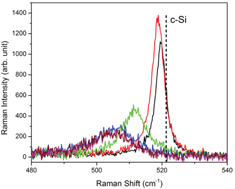
Figure 1. Raman spectra of 1.5 MeV Au implanted Si sample at different ion fluences. The dotted line indicates Raman peak position of c-Si.
Download figure:
Standard image High-resolution imageWe have also carried out Rutherford backscattering (RBS) measurements using 1.35 MeV He+ ions at a backscattering angle of 160°, on these samples. Figure 2 shows the RBS spectra of only Au profile for different ion fluences. It shows Au presence at a depth of around 170 nm from the surface and spread over around 350 nm. Upon annealing at 500 °C, Au out-diffuses toward the surface. As the penetration depth of the probing laser beam in Raman scattering measurements is much less than the range of Au, it does not detect Au atoms. However, it can characterize the damage created by Au2+ ions. The Raman peak position and linewidth variation with implantation fluence is shown in figure 3. The red-shifting of peak position and linewidth broadening shows similar behavior/trend with increasing implantation fluence. At and above 5 × 10¹⁴ ions cm−2, the peak shift and line-width broadening seems to saturate. Let us now try to understand the origin of the observed shift. It is well known that stress present in the system leads to a shifting of Raman peak toward the lower or higher wavenumber, depending on the nature of stress, i.e. tensile or compressive, respectively. The Raman scattering measurement is used to determine the mechanical stress from the shift of the 521 cm−1, Si Raman phonon mode. This phonon mode is known to be very sensitive to lattice strain [13]. Moreover, it has been experimentally observed that MeV ion implantation produces uniaxial stress in the system [14]. In view of the above, we assume in our case, stress is present in the system due to Au2+ ion implantation. We have calculated the stress present in the system due to ion implantation for different ion fluences. The magnitude of the stress can be estimated from the shift in Raman peak position, Δωs [15]

where σ is the magnitude of the stress. The stress magnitudes for different ion fluences have been summarized in table 1. But it is also very important to note that due to stress there should not be any linewidth broadening. In contrast, in the present case we observe both peak shift as well as linewidth broadening.

Figure 2. Rutherford backscattering spectra showing Au profile for different ion fluences.
Download figure:
Standard image High-resolution image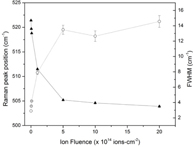
Figure 3. Raman peak position and line-width variation with ion fluence.
Download figure:
Standard image High-resolution imageTable 1. Stress values calculated for various ion fluences. Raman peak position is also shown for comparison.
| Ion fluence (ions cm−2) | Raman peak position (cm−1) | Tensile stress (calculated) (GPa) |
|---|---|---|
| 5×10¹² | 519.7 | 0.332 |
| 1×10¹³ | 518.8 | 0.553 |
| 1×10¹⁴ | 511.2 | 2.37 |
| 5×10¹⁴ | 505.2 | 3.968 |
| 1×10¹⁵ | 504.6 | 4.100 |
| 2×10¹⁵ | 503.9 | 4.275 |
Another reason for peak shifting and broadening as explained in literature could be due to quantum confinement effect. In the case of bulk crystalline Si, the optical phonons close to the zone center q ∼ 0 are contributing to the Raman spectrum. This q ∼ 0 selection rule is essentially a consequence of the infinite periodicity of the crystal lattice. But, when the periodicity of crystal lattice is interrupted, as in nanocrystals, this rule is relaxed and the phonons away from the Brillouin zone center, depending on the size of nanocrystals, also contribute to the phonon/Raman lineshape [8, 9]. This resulted in an asymmetric peak at lower wavenumber as compared to 521 cm−1. In the present case, we observe peak shift with broadening but the shape of the spectrum looks symmetric. Thus, we believe, this shifting and broadening in the present system are both due to stress and confinement effect. This can be further clarified in the following sections. In another context, we know that ion implantation produces damage in the target matrix which gets amorphized at higher implantation fluence. There are many models explaining the mechanism of amorphization. One of the well accepted models for this is the overlap model/heterogeneous amorphization. According to Brinkman [16], when the cross section for displacement collisions becomes sufficiently large for a moving ion to displace one target atom per lattice plane, the volume affected is melted for a short period of time and then rapidly quenched. Such volumes are called displacement spikes [16] and are presumed to anneal into small dislocation loops plus clusters of interstitial and vacancies as a result of the rapid quenching. When this occurs in a small volume, the characteristics of the material change toward the amorphous state [17]. In line with the above, it has been experimentally observed that a single O+ ion impact creates an a-Si nano-zone in the implanted layer of c-Si [18]. Such amorphous zones have been directly observed by transmission electron microscopy (TEM) for low fluence ion bombardment in Si [4]. In the present case, as the Au2+ ions are much heavier compared to O+ ions, we expect similar amorphous nano-zone formation in c-Si. While passing through the c-Si, Au ions locally deposit their energy (nuclear stopping power, Sn for 1.5 MeV Au in Si 2.693 × 10² eV A−1) which results in amorphous patches (nano-zones) in crystalline Si.
To explain the red-shift in Raman peak position and linewidth broadening with respect to ion fluence here we propose a model taking both stress and quantum confinement into account. We believe, the Raman signal comes from the crystalline area present between the amorphous patches (a-Si nano-zones). As the ion fluence increases, the diameter/space between the amorphous nano-zones (i.e. the crystalline patches) goes on decreasing, as shown in the schematic diagram, figure 4. The above model is very similar to that of porous silicon. As in the case of porous Si, here the pores are replaced by a-Si nano-zones. The crystalline regions between a-Si nano-zones are stressed due to the presence of amorphous Si in their vicinity. This may be the reason for the symmetric peaks instead of asymmetric as a consequence of quantum confinement effect. The same kind of observation has been reported in the case of Si nanocrystals in the vicinity of gold-silicide structures [19]. It has been observed that the thermal annealing of isolated amorphous zones recrystallizes at lower temperature than the continuous amorphous layer [20]. Donnelly et al [20] have recorded the images of the dynamical shrinkage of the individual zones monitored by slowly ramping up the temperature. In line with the above, we observe that the annealing at 500 °C of a sample implanted with 2 × 10¹⁵ ions cm−2, results in a blue shift in Raman peak position from 504 to 508 cm−1, toward the 521 cm−1 crystalline peak. This is primarily because of stress relaxation or, in other words, recrystallization of amorphous nano-zones due to thermal annealing at 500 °C.
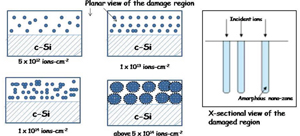
Figure 4. Schematic diagram showing the change in implanted region with respect to the ion fluence.
Download figure:
Standard image High-resolution imageX-ray diffraction (XRD) measurements carried out on these samples support the above proposed model. Grazing incidence XRD (GIXRD) measurements were carried out at an incidence angle of 3°, to see the effect of implantation fluence on the surface. Figure 5 shows the XRD spectra of the implanted samples corresponding to three implantation fluences viz. 1, 5, 10 × 1014 ions cm−2. We observed a very broad peak located at 23°, which indicates that there are some amorphous materials present in the system. In addition to this, another broad peak at 57° has been seen which corresponds to Si(311) plane. The broadness (FWHM ∼ 3°) of 57° peak indicates the presence of nanocrystalline patches in the system. As the implantation fluence increases, the intensity of the observed broad peak at 57° decreases. This is mainly because with increasing fluence, the area between the amorphous zone (i.e. the nanocrystalline patches) goes on decreasing, which results in decrease of XRD peak intensity. Thermal annealing of the sample (fluence 2 × 10¹⁵ ions cm−2) at 500 °C resulted in an intense narrow peak at 57° as compared to that of the as-implanted samples. This is shown in figure 6. This observation is also in line with the above analysis of re-crystallization or relaxation of the stress present in the system due to implantation.
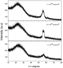
Figure 5. XRD spectra of as-implanted samples corresponding to three different ion fluences 1 × 10¹⁴, 5 × 10¹⁴ and 1 × 10¹⁵ ions cm−2.
Download figure:
Standard image High-resolution image
Figure 6. GIXRD spectrum of an annealed sample, 2 × 10¹⁵ ions cm−2.
Download figure:
Standard image High-resolution image
4. Conclusion
In this paper we have investigated the effect of 1.5 MeV Au2+ implantation in crystalline silicon mainly using Raman scattering method and XRD. There is a red-shift in Raman peak position and line-width broadening with increasing implantation fluence. The origin of the observed red-shift and line-width broadening are explained with the help of a proposed model. These changes are due to both stress and quantum confinement effect. The amount of tensile stress produced due to implantation, as a function of fluence, are estimated. A direct analogy has been drawn between porous Si and the present implanted system. This study gives a new insight to study the Raman scattering results of the implanted samples.
Acknowledgments
The author thanks A K Behera and the technical staff of IOP, Bhubaneswar (IOPB) for their invaluable technical help in the irradiation experiments. The author also thanks Professor T Som and Tanmoy Basu for the help during XRD measurements at IOPB. The author acknowledges DST, Government of India, for the funding under DST Fast Track Scheme for Young Scientists, Project no. SR/FTP/PS-007/2012.