
Abstract
A process flow using photolithography and sputtering was studied for copper antenna fabrication on thin poly(ethylene terephthalate) (PET) substrate. The lift-off route was chosen for its flexibility at laboratory scale. It was clarified that the cleaning of PET is an important step that necessitates mild oxygen plasma etching. Then copper is sputter deposited after photolithographic definition of the antenna. Care is necessary since PET, as a very flexible substrate, is temperature sensitive. The temperature increase generated by the impact of deposited copper should be maintained below the glass transition temperature of the polymer to avoid detrimental deformation. dc power of 40 to 50 W was found to be the maximum possible sputtering power for commercial PET. It was found that the resistivity of the thin film is below two times the bulk resistivity of copper for a deposition pressure below 4×10⁻³ mbar and thickness above 450 nm. These results enable the reliable fabrication of copper RFID UHF antennae on a PET substrate for further testing of new tag designs. The present paper summarizes the effort to test new designs of antennae for RadioFrequency IDentification (RFID) Ultra High Frequency (UHF) tags, for use in various applications (e.g. object tracking and environment monitoring) in Vietnam.
Export citation and abstract BibTeX RIS

Content from this work may be used under the terms of the Creative Commons Attribution-NonCommercial-ShareAlike 3.0 licence. Any further distribution of this work must maintain attribution to the author(s) and the title of the work, journal citation and DOI.
1. Introduction
RadioFrequency IDentification (RFID) technology has been developing for some time now and entered commercialization in the last decade of the 20th century [1]. It primarily consists of tags fixed to objects that can be read using radiofrequency waves. The objects are generally moving and the reader is fixed, but the reader may be mobile and the objects fixed. The tags are usually made of an IC chip connected to an antenna. They hold information in the chip's memory, which can be anything from an identification number to the complete history of an associated sensor. The only limit is the size of the memory, which is usually relatively small due to cost constraints. In fact, the price of a tag is one of the primary factors [2] hindering the extensive use of this technology to replace barcodes for product identification. Another important factor that limits their use is their sensitivity to the environment. In proximity to liquids or metals, the reading of most tags is severely affected. Our research programme is aimed at improving both factors.
Most tags are fabricated on flexible substrates. Aside from the low-cost goal, this comes from the necessity to adapt to various object surfaces, such as cardboard boxes, plastic bottles and heterogeneous surfaces, while being easily laminated with an adhesive layer. The work presented here is aimed at the development of a fabrication process for laboratory purposes. This would allow for the fabrication of small quantities of tags for testing new designs, the laboratory being equipped with the complete set of tools, from simulating the tags with electromagnetic software to testing the chip's impedance and measuring the tag through the reading operation.
The Ultra High Frequency (UHF) range (from 860 to 960 MHz) is chosen as the most useful frequency range for RFID applications. The higher reading range (up to several meters) is the key for many applications [3]. Furthermore, it is relatively straightforward to design compact antenna which allows for practical fabrication with the available microfabrication tools.
A tag is composed of an antenna deposited on a flexible substrate to which an IC chip is connected. The antenna provides the transformation of the incoming electromagnetic wave to electrical power for the chip. It is also the means of channeling data to the chip. The chip should be low cost and standardized in order to be compatible with the existing infrastructure. The most interesting part of the tag is the antenna, since this makes it possible to adapt the tag to every application of interest—a step that is still absolutely necessary due to the absence of a universal tag. Once the size constraint is fixed, one of the main parameters to adjust when designing such an antenna is to match its impedance to the given impedance of the chip. As this is partly influenced by the processing of the antenna, it is usually not possible to finely tune the impedance of the antenna by electromagnetic simulation alone. Therefore, a simple low cost fabrication process at the laboratory scale is absolutely mandatory for demonstration purposes, where it will be possible to modify the antenna design for good matching.
Antenna fabrication is described, starting with the structure of tag, the cleaning and photolithography steps, followed by copper sputter deposition study. It is shown that the maximum temperature generated by sputtering is predictable using a simple model. Then properties of the obtained copper thin films are detailed.
2. Experimental
2.1. Tag structure
The tag is fabricated on commercially available 80 μm thick poly(ethylene terephthalate) (PET) film. The main advantage of this material is its low cost among the plastic films while keeping good mechanical and thermal properties. PET does not degrade thermally up to 200 °C, although its glass transition temperature is in the range of 80–100 °C, depending on the exact fabrication process. This temperature is sufficiently high to allow for standard microfabrication processes. A slightly higher temperature can be applied (up to 150 °C) for a reasonably short time (up to 5 mins) without detrimental damage to its mechanical properties.
An efficient UHF antenna needs to have a thickness equal to the penetration depth of electromagnetic wave in this range. Processing copper by sputtering can be followed by electrodeposition to obtain the required thickness at low cost. This is not possible with aluminium, which presents the same good characteristics of low resistivity and low cost. Subtractive processing from metal foil on polymer film presents attractive features, such as low cost and relatively fast development. Nevertheless, the choice of polymer film is relatively limited. This last point is unattractive for longer term development, where we need to keep the highest flexibility in our choice of flexible substrate. Therefore, copper was chosen as the most practical metal to develop the present fabrication process.
2.2. Photolithography process
Commercial PET surface quality greatly differs from a high quality silicon surface. Its surface is rough, with scratches and usually contaminated with organics due to handling. Prior to using this material, it is therefore mandatory to clean it. This is done with acetone and ethanol baths at ambient temperature, followed by rinsing with deionized water and drying at 90 °C for 3 mins. This simple procedure was considered sufficient at first but, as is shown in figure 1, lacks of copper appear randomly on the PET surface despite great care taken in photolithography development and copper sputtering.
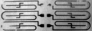
Figure 1 Examples of copper lacks observed on final samples without oxygen plasma cleaning.
In order to solve this specific problem, mild etching of the PET surface was performed prior to photoresist spinning. Conditions for etching in Oxford Instrument Plasmalab 80 Plus Reactive Ion Etching (RIE) equipment are 265 W of radiofrequency power in a pure oxygen atmosphere at 50 mTorr during 3 mins. As is well known, oxygen plasma tends to enhance the wettability of polymer surfaces [4, 5] by breaking surface bonds and providing free dangling bonds for subsequent deposited layers. The effect achieved by such treatment lasts reasonably long (at least several hours) for good reproducibility.
All experiments are carried out on 4'' square PET films. To keep this material flat during the different processes, it was fixed at the corners to a 4'' square glass wafer. It was checked that this way allows for good behavior during the complete process.
The basic lift-off process uses photoresist as a mask for definition of the patterns to be deposited. Subsequent removal of the photoresist mask (usually in acetone) leaves the deposited material on the desired locations. One of the difficulties of this process lies in pattern edge definition. As the deposited material over the photoresist mask partly covers the edge, even with anisotropic deposition processes like sputtering, the clean removal of the photoresist mask is difficult in practice due to this bridging. To solve this problem, a specific underlayer can be used. Such lift-off resist (LOR) was purchased from Microchem (USA). This layer is first spinned on the surface followed by a standard photoresist (in this study, an i-line photoresist from Fuji Film, OiR 917/17 or OiR 917/12). During development of the photoresist, the developer induces a small overetch of the LOR, providing an undercut. This forms a cap, which does not allow a continuous layer to grow on the pattern edge, thus avoiding problems when removing the photoresist mask.
The LOR and i-line photoresist are subsequently spinned and baked. The parameters are as indicated in table 1.
Table 1. Process parameters for LOR and i-line photoresist.
| Dispense | 500 rpm for 7 s | 500 rpm for 7 s |
| Spinning | 4000 rpm for 30 s | 4000 rpm for 30 s |
| Bake | 150 °C for 5 min | 95 °C for 1 min |
Exposure of the photoresist is done using a MJB4 mask aligner (Suss Microtech) in contact mode. The selected wavelength is 365 nm. The mask used is a flexible mask produced by offset printing. The measured resolution is better than 15 μm and the edge roughness on straight lines is below 5 μm. These figures are accurate enough for all possible antenna in the UHF range, the minimum planar dimension always being larger than 100 μm. The mask is fixed on a 5'' glass wafer and placed on the mask holder of the mask aligner. In order to ensure a good contact between the 2 soft materials, the hard contact mode of the equipment is used. Exposure was fixed at 7 s after optimization to take into account the transparent PET substrate and glass support. A postbake at 120 °C during 1 min helps to stabilize the photoresist before development is done for 100 s in an MF319 developer purchased from Rohm and Haas.
A study was conducted to check for the accuracy of the pattern dimensions after exposure. It was found that the transferred pattern has the dimensions of the mask within the accuracy of the measurement under the microscope, i.e. below ±1 μm.
2.3. Sputtering process
Compared to other processes to deposit metals, sputtering presents the advantages of low resistivity of the deposited layer [6, 7] as well as good adhesion due to the relatively high impact energy of the sputtered species. This specific feature is of great importance when one attempts to deposit metal on a polymer. It is well known that metal does not adhere very well to polymer materials. At the same time, the higher impact of deposited atoms enhances the chemical interaction with the polymer surface.
The sputtering equipment used is a Leybold Univex 350 with a 2'' sputtering gun. Due to the configuration of the chamber to allow for several guns, the copper target does not face the substrate holder. Rather, the head is angled and the center of the target faces the middle of the 4'' substrate holder radius. This specific configuration was chosen so as to obtain the highest possible homogeneity over the 4'' substrate when it is rotated during deposition. The distance between the center of the target and the substrate holder along the axis of the sputtering gun is 100 mm. dc sputtering mode is used.
The first study was conducted to assess the temperature increase caused by the sputtered species. When depositing metal on a polymer substrate, it is important to know parameter in order to avoid thermal deterioration of the substrate. This was conducted by placing a thermocouple on the substrate holder facing the center of the target. It was found that, for power between 40 and 50 W, the maximum temperature reached is between 105 and 130 °C, depending on the deposition pressure. At the same time, it was clarified that the system can be modeled easily, considering that the sputtering source provides a constant flux of sputtered species on the substrate, which dissipates the heat through the substrate holder axis by thermal diffusion. This allows one to predict the limit temperature, which is of great value for reliably processing the copper thin film on PET without damage.
The second part of the study aimed to determine the resistivity of the copper thin film in this power range, for pressures in the range of 1.7×10⁻³ mbar (the lowest pressure for stable discharge) and 5.8×10⁻³ mbar (maximum reachable pressure with the chosen experimental conditions) and various thicknesses up to 1.1 μm. This study was conducted on 4'' glass square wafers. Resistivity measurement by a 4 point prober on PET suffers some inaccuracy due to the soft underlying polymer. Checks were made on PET too and the same order of magnitude of resistivity was confirmed. The glass substrate was masked to obtain 16 squares over the surface in order to check for thickness as well as resistivity homogeneity. The size of the squares is chosen to allow for 4 point prober measurements, which require enough area between the probe and the edge of the pattern to be measured.
Finally, adhesion of copper on PET was assessed with a standard scotch tape test. Twenty five squares of 1 mm side are defined on the PET surface by cutting the copper thin film with the tip of a cutter. Scotch tape is strongly pressed on this area and subsequently removed slowly. No delamination was observed and no defect was detected under the microscope, confirming the good adhesion of sputtered copper on PET.
3. Results
3.1. Temperature during sputtering
The temperature increase of the substrate during sputtering can be understood as a result of the response to the onset of a heat source (step function) due to bombardment by the sputtered species. The thermal inertia of the substrate holder and its evacuation of heat by diffusion through its axis linked to the rotation motor explain the main features of a typical temperature versus time profile, shown in figure 2. More specifically, this profile is similar to a second-order system submitted to an external input in the form of a step function.
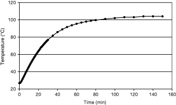
Figure 2 Example of temperature profile during sputtering at 40 W and 2.2×10⁻³ mbar.
The details of analysis are described in appendix A. Table 2 presents the relevant identification parameters. The last 2 columns are the minimum and the maximum of the difference between experimental data and computed profile.
Table 2. Process parameters for LOR and i-line photoresist.
| 40 | 1.8 | 26.7 | 112 | 48.1 | 21.2 | 2.8 | −1.0 | 1.4 |
| 40 | 2.2 | 29.1 | 105 | 49.4 | 28.5 | 2.2 | −1.3 | 1.7 |
| 40 | 2.9 | 26.8 | 112 | 44.4 | 25.0 | 2.0 | −1.8 | 1.5 |
| 40 | 4.2 | 28.1 | 104 | 43.2 | 24.8 | 1.9 | −1.3 | 1.0 |
| 50 | 1.7 | 28.2 | 123 | 38.9 | 18.7 | 2.1 | −1.7 | 1.3 |
| 50 | 1.95 | 40.5 | 124.5 | 45.3 | 22.8 | 2.3 | −0.8 | 1.0 |
| 50 | 2.9 | 39.5 | 129.5 | 42.9 | 21.6 | 2.2 | −0.9 | 1.4 |
| 50 | 4.3 | 46.7 | 105.5 | 32.2 | 16.7 | 1.6 | −1.7 | 0.5 |
It is verified that no correlation exists between initial and limit temperature, which is expected for a system with a constant power source. There is a trend of higher limit temperature for higher power, but at the same time a visible decrease in limit temperature at higher pressure. This last effect is understood as a result of the scattering of the sputtered species, which brings less energy to the substrate. The time constant τ1 is slightly less for higher power, indicating a faster heating process. It can be seen in table 2 that the identification leads to an estimate of the limit temperature better than ±2 °C. This result is enough for the safe prediction of sputtering conditions on PET.
3.2. Resistivity
Figure 3 shows the effect of deposition pressure on thickness and resistivity for samples deposited at 40 W for 75 mins and 50 W for 60 mins. Those deposition times were chosen to get enough thickness for reliable measurement, as well as almost equivalent values for power for comparison purposes.
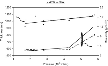
Figure 3 Average thickness and resistivity of copper thin films at 40 W for 75 min and 50 W for 60 min.
A slight trend of thickness increase with pressure is observed. This is the result of a competing effect. The increased deposition pressure induces an increase in the scattering of sputtered species by the denser plasma, which therefore tends to deviate or stop the sputtered species. However, at the same time, the argon ion density being larger, the sputtered species is increased. This phenomenon is observed in the literature [6], but most of the time is neglected compared to the decrease in deposition rate at pressures higher than our range, resulting from the much greater effect of the scattering by dense plasma.
The resistivity of the present thin films increases sharply above 4.5×10⁻³ mbar, as observed in other works [6, 7]. However, the resistivity at low pressure in this study is lower than found in equivalent studies in the literature [6, 7] and independent of deposition pressure. The trend in power, however, is similar with that observed elsewhere, with a smaller increase in resistivity at higher power. The average resistivity below 3×10⁻³ mbar is between 2.1 and 2.6 μΩ cm.
A study of the influence of thickness on the resistivity shows a general decreasing trend, as shown in figure 4. The smallest resistivity is 2.1 μΩ cm.
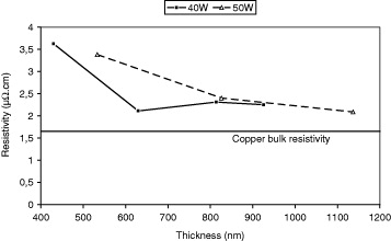
Figure 4 Thickness effect on resistivity of thin films sputtered at 1.8×10⁻³ mbar.
The sheet resistance measured by the 4 point prober is in the same range as the calibration sample (a silicon wafer with controlled resistivity), ensuring good accuracy. Nevertheless, a large variability in the sheet resistance measurements is reflected in the resistivity results. The variability in the results is partly due to the variability of the measurement of sheet resistance by the 4 point prober. The mean thickness variability over all samples is 5.9% and 5.4% for 40 and 50 W, respectively, while the mean resistivity variability is 15.4% and 12.2%. On the thinner samples, it can reach up to 23%, where the thickness variability never exceeds 9.5%. No correlation is found between thickness and resistivity variations in the different samples. On average, over the 16 measurement points of each sample, the general trend is to slightly lower variability at lower pressure and higher power. Over a 4'' substrate sputtered by a 2'' target, these results are well suited to the purpose of antenna fabrication.
3.3. Antenna
After sputtering copper in a controlled manner, the PET film is dipped in an acetone bath at room temperature. PET being insensitive to this solvent, it is possible to wait for slow dissolution of the underneath photoresist mask. The final result is shown with several antenna designs in figure 5 (the connection pads have the same size on all antenna but the scale of the photos may slightly vary). It is clearly visible that all processed antennae are properly defined with no defects, whatever different features they exhibit.
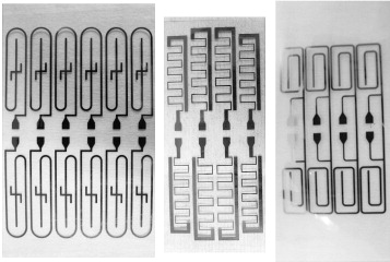
Figure 5 Examples of RFID UHF antennae processed along the described process flow.
4. Outlook
This experimental work aimed to explore conditions for fabricating RFID tags on flexible substrates. Standard microfabrication tools, namely photolithography and sputtering, were used for antenna fabrication. It was shown that high quality copper antenna can be fabricated on a thin PET substrate with no damage to this supporting layer. The best copper resistivity is only 25% higher than the bulk copper resistivity. It is also maintained below twice its bulk resistivity for deposition pressures below 4×10⁻³ mbar and thicknesses above 450 nm. This process window provides a good margin for processing high quality antennae for RFID UHF tags.
By acquiring fundamental knowledge of fabricating tags on flexible substrates, the main parameters are being understood that will greatly help further improvements. This will allow for the production of tags with different IC chips, any antenna shape and, in the future, new flexible substrates, such as polyesters or other polymer films.
The next step is to process the connection between the chip and the antenna in order to obtain a reliable tag, this connection being the most critical part of a working tag due to its inherent fragility. This will be studied in parallel with the thickening of the copper layer by electrodeposition. This last process provides high quality copper at low cost and is especially suited even to large-scale production. This progress will allow for the implementation of a new design, subject to current work undertaken at the Laboratory for Nanotechnology, Vietnam National University, Ho Chi Minh City.
Acknowledgments
The financial support of the Vietnam National University at Ho Chi Minh City is acknowledged. Pr Tedjini (Laboratoire de Conception et Intégration des Systèmes, Grenoble-INP, Valence, France) provided one of the antenna designs.
Appendix
System identification is a common procedure for modeling physical systems [8]. It is often used when modeling the physical system is complex and requires a knowledge of parameters that are difficult to measure. Especially for system with simple behavior, like temperature increase during the sputtering process, we search for a first- or second-order linear model. For thermal systems with slow variation, transient time-domain analysis is better suited to system identification. Given the shape of the response shown in figure 3 (horizontal tangent at start, no overshoot), a second-order model is expected with overdamped characteristics. In this case, the following form of the model is forecast.

where T is the temperature at substrate level, T0 is the temperature before submitting the substrate to the plasma, T∞ is the temperature after an infinite process time, p1, p2 and K are expressed by

m and ω0 being the parameters in the second-order linear differential equation

with the step function Γ(t) vanishing before the start of the experiment.
To identify the two parameters of the differential equation, the relatively limited sampling rate of our temperature data favors a time identification using the following procedure. The tangent to the temperature at the inflexion point is determined. It is used to determine the time TB between the inflexion point and the horizontal line corresponding to the limit temperature. A second time TA is determined between the cross points of this tangent to both horizontal lines at the starting temperature and at the limit temperature. The ratio TA /TB is univocally related to the parameter α. However, the accuracy of this ratio computed from the data is insufficient to reach a satisfactory fit. α is therefore kept variable. Then the following relations are used to compute the parameters:

The limit temperature T∞ is, in practice, unknown precisely. Therefore, the parameters α and T∞ are adjusted iteratively so as to obtain the best match between data and calculated curves for the temperature profile and its slope. An example of results from such a procedure is given in figure A.1.
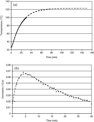
Figure A.1 Data and computed fits for a temperature profile at 50 W and 1.7×10⁻³ mbar (a) temperature profile and (b) slope.
It should be noted that the accuracy of this transient analysis is limited by the noise sensitivity of the method [8]. The obtained accuracy, however, is good enough to predict the limit temperature of the process for a given power and deposition pressure within ±2 °C.
Finally, in table 2, the period corresponds to the inverse of the pseudo-pulsation ω0, and the time constants τ1 and τ2 are the negative inverses of p1 and p2, respectively.