
Abstract
Silicon nanostructure-based light emitting devices (nc_SiLED) have been fabricated using conventional microelectronic technologies. The emissive layer composed of silicon and silicon dioxide was deposited by magnetron co-sputtering. Under forward bias, a broad electroluminescence (PL) spectrum in the range 450–900 nm was observed, peaking at around 705 nm. The effect of Si content in the active layer on the electrical and optical properties of these devices was measured and discussed.
Export citation and abstract BibTeX RIS

Content from this work may be used under the terms of the Creative Commons Attribution-NonCommercial-ShareAlike 3.0 licence. Any further distribution of this work must maintain attribution to the author(s) and the title of the work, journal citation and DOI.
1. Introduction
The development of Si-based photonics has lagged far behind the development of electronics for a long time. The main reason for this slow progress has been the lack of practical Si light sources, i.e. efficient Si light-emitting diodes (LED) and injection lasers. Si is an indirect-band-gap material. Light emission in indirect materials is naturally a phonon-assisted process with low probability (spontaneous recombination lifetimes are in the millisecond range). In the bulk Si, competitive non-radiative recombination rates are much higher than the radiative ones and most of the excited e–h pairs recombine non-radiatively. This results in very low internal quantum efficiency (η i ≈10−6) of Si luminescence [1]. At a higher pumping rate, the Auger effect strongly prevents population inversion, which is necessary to achieve optical amplification.
During the last 20 years, many different strategies have been employed to overcome these material limitations. Present day Si LEDs are only a factor of ten away from the market requirements, and optical gain has been demonstrated [2–4]. The availability of Si nanotechnology played a primary role in these achievements. It is known that electronic states in Si nanocrystals (Si-NC) are strongly influenced both by the quantum confinement (QC) effect and by the formation of additional surface states [5–7]. The QC effect is a rearrangement of the density of electronic states in energy as a direct consequence of volume shrinking in one, two or even three dimensions, which can be obtained, respectively, in quantum wells, quantum wires and quantum dots. On the other hand, the arrangement of the atomic bonds at the surface also strongly affects the energy distribution of electronic states, since in Si-NCs silicon atoms are either at the surface or a few lattice sites away. The QC and a suitable arrangement of interfacial atomic bonds can enhance radiative recombination efficiencies in Si-NCs by orders of magnitude and, in some cases, optical gain can be observed [4].
Research on silicon-based light emitting diodes (LED) has attracted great interest from scientists [8–16]. The light emission in bulk silicon-based devices is constrained in wavelength to infrared emission, and in efficiency by the indirect band gap of silicon. Porous silicon and Si-NCs have higher luminescent efficiency in the visible region, so they have been investigated intensively recently. A critical challenge for devices based on Si-NCs embedded in a silicon dioxide matrix is the way to inject both kinds of carrier into the NCs. Walters et al have proposed a scheme for electrically pumping charge carriers into an array of Si-NCs by the field effect electroluminescence mechanism [8]. In this excitation process, electron and hole are alternately injected into the Si-NCs layer through the potential barrier by tunnel process, instead of the charge carrier simultaneous injection into the p–n junction in the conventional LED. This model requires a complex structure, similar to the structure of the field effect transistor, consisting of source, drain and gate electrodes. Furthermore, in order to ensure the light emission of the device, the power supply must be designed in such a way that the frequency and voltage of the applied pulses can be controlled.
Another method to excite the Si-NCs is the use of the impact ionization process in which hot electrons create the carriers (bound excition) when suitable voltage is applied to the electrodes of the device [9, 10]. In such a process, the excess energy of the hot carrier is converted to heat, which reduces the efficiency and lifetime of the device. Despite these disadvantages, many kinds of Si-NC light emitting devices have been investigated based on this excitation principle.
In this paper, the fabrication, working principle and electroluminescence properties of the silicon nanostructures based light emitting device are discussed.
2. Experimental
2.1. Deposition of the active layer
(100) oriented p-type Si wafers with resistivity of 5–8 Ω cm were used as starting materials. Before the deposition, the Si wafers were dipped in 1% hydrofluoric acid to remove the surface native oxide, rinsed with a large amount of de-ionized water and dried by a spinner. SiO 2 : Si films (active layers) were deposited on the substrates by rf magnetron co-sputtering of silicon and silicon dioxide. The content of Si in the produced SiO 2 : Si films was from 10% to 14.5%, controlled by the number of silicon chips placed on the SiO 2 target. Then, the formation of Si-NCs was achieved by annealing the films at 1000 °C in a N 2 atmosphere for 60 min.
2.2. Device fabrication
The devices were fabricated using conventional microelectronic technology. The structure of Si-NC LEDs is illustrated in figure 1. The thickness of the SiO 2 layer and the active layer (SiO 2 : Si) were 40 and 400 nm, respectively. An Al film of 800 nm thickness was thermally evaporated and annealed for 30 min at 450 °C in vacuum to form the back contact. A 150 nm thick indium tin oxide (ITO) layer was sputtered and annealed for 30 min at 450 °C in vacuum to make the top transparent electrode.
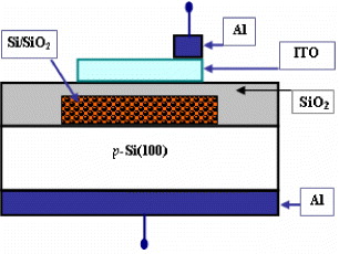
Figure 1 Schematic illustration of the Si-NC LED structure.
3. Results and discussion
After fabrication, each single Si-NC LED chip was cut off from the wafer and the electrodes were welded. Figure 2 shows a photograph of a typical Si-NC LED device.
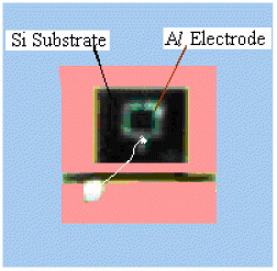
Figure 2 Photograph of a typical Si-NC LED device.
In order to investigate electrical properties of the device, current–voltage (I–V) characteristics were measured between its back and front contacts. By defining positive and negative, the voltage applied under forward and reverse bias, respectively, we present in figure 3 the I–V characteristics of the devices with different Si content in the active layers. For all the devices, the thickness of the active layer is 400 nm. The Si content in the active layers of the device A, B and C are 10, 12.5 and 14.5%, respectively.
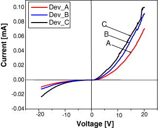
Figure 3 I–V characteristics of Si-NC LED with different Si content in the active layer.
It is known that the crucial step in fabricating a light source based on a Si/SiO 2 co-sputtered active layer, or in other words, Si-NCs embedded in SiO 2, is to make the carrier injection in a semi-insulating material possible. Let us first consider the transport process in the case where the Si-NCs are distributed uniformly in the silica matrix. When a forward bias is applied to the electroluminescent device, all the bias potential drops on the matrix layer, the carriers can jump from one NC to the other by a tunneling process and a small direct tunneling current appears. When the bias voltage increases above 5 V, the current flowing though the sample increases super-linearly, as a result of the combined process of the Fowler–Nordheim (FN) injection for the case of a triangle barrier [1] and the impact ionization of hot electrons.
When the negative potential is applied to the semiconductor side electrode, the device is not conducting, since p-type silicon has no electron. Hence the current flow in the case of negative bias is very small.
From figure 3 we can see that, by increasing the Si content in the active layer, there is an increase in the current that can pass through the device for the same applied voltage. In fact, by increasing the silicon content, the density and the mean radius of NCs also increase. The larger Si-NCs have a smaller band gap and, moreover, by increasing the density of Si-NCs, their mean distance decreases and therefore the efficiency of the tunneling effect increases.
The EL measurement of the devices was carried out at room temperature. The EL spectra of three Si-NC LED devices with different Si content of 10% (DEV_A), 12.5% (DEV_B) and 14.5% (DEV_C) are depicted in figure 4. Under the forward voltage of 15 V, the Si-NC LED emitted quite intense visible light that can be seen with the naked eye through transparent ITO film. The light emission is stable and reproducible. As depicted in figure 4, for all devices the emission resulted in a broad-band spectrum distributed from 450 to 900 nm with a single peak at around 705 nm. The intensity of EL peak decreases with the increase in the amount of Si in the active layer. However, no clear shift of the EL spectrum with Si content is observed.
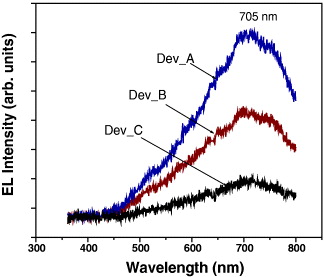
Figure 4 Decrease in EL intensity with higher Si content in the active layer.
Figure 5 shows the EL and PL spectra for the device based on an active layer with 10% Si (annealed at 1000 °C, 60 min in N 2). The EL spectrum was measured by biasing the device with 15 V (current density 0.075 A cm −2). The PL measurement was carried out by exciting the 325 nm line of a He–Cd laser through the top contact of the device. As can be seen in the figure 5, the maximum of the EL and PL emission bands are very close to the wavelength, around 705 nm. However, the band-width of the EL spectrum is broader compared to that of the PL spectrum. The reason for this difference is understood, as follows. During the EL measurement, no lens was used, so the recorded signal was the integration of all the lights coming from different dots (from 1 mm 2 of device surface). In the case of PL measurement, only the NCs under a small laser spot were excited and their PL emission was recorded. From this direct comparison, it is possible to attribute the red-light emission of both EL and PL to the electron-hole recombination in the Si-NCs (although the excitation mechanism is different) [6, 7, 17–21]. In fact, the excitation under electrical pumping is due to the impact of hot electrons accelerated by the electrical field. This phenomenon generates the e–h pairs in the Si-NCs, and the radiating recombination of e–h pairs determines the light emission.

Figure 5 Comparison between the EL and PL spectra of the Si-NC LED device with Si content of 10%.
4. Conclusions
We have studied the structural, electrical and optical properties of silicon nanostructure-based light emitting devices (nc_SiLED) fabricated using microelectronic technology. The active layer of the device was obtained by co-sputtering silicon and silicon dioxide with Si content varying from 10 to 14.5%. Under the same applied voltage, the intensity of EL decreases with the increase in the Si content. The EL intensity is very stable and visible to the naked eye, with the emission wavelength centered at ∼705 nm. The EL and PL peaks are very similar in position, though broader band-width is observed for EL emission. The EL is most probably excited by the impact excitation of electron–hole (e–h) pairs in Si-NCs that were formed in the active layer of the device after annealing.
Acknowledgment
This work was financially supported by the National Foundation for Science and Technology Development (NAFOSTED), Vietnam, under project nos 103.02.102.09 and 103.02.83.09.