
Abstract
An ultrabroadband far-infrared absorber is achieved using an anisotropic metamaterial composed of alternating black phosphorus (BP) and dielectric films arranged in a trapezoidal structure. We numerically demonstrate that ultrabroad bandwidths (with >90% absorptivity) can be achieved with the strong anisotropic dielectric response of BP, namely 63.6 μm along the armchair direction and 53.6 μm along the zigzag direction. Importantly, the high absorption is maintained across a wide range of incident angles. Our simulation results align well with analytical calculations based on the effective medium theory, considering the multilayer structure as an effective homogeneous metamaterial with anisotropic permittivity. From the distribution profiles of magnetic fields, we observe tight trapping of different wavelengths at varying widths of the trapezoidal absorber, revealing the slow-light effect underlying the broadband absorption. Our study holds significant potential for device applications, such as BP-based broadband infrared photodetectors.
Export citation and abstract BibTeX RIS

Original content from this work may be used under the terms of the Creative Commons Attribution 4.0 license. Any further distribution of this work must maintain attribution to the author(s) and the title of the work, journal citation and DOI.
1. Introduction
Metamaterial absorbers (MAs), capable of strongly absorbing incident electromagnetic radiation, have become essential components in various applications, such as thermal emitters [1], sensors [2], detectors [3], nonlinear devices [4], etc. Previously, Landy et al first proposed a thin MA to realize single-wavelength perfect absorption [5]. Since then, similar concepts have been applied across a wide frequency band, ranging from the microwave to terahertz and visible light [6–18, 19]. However, many MAs generally exhibit narrowband absorption, limiting their optical properties, including broadband light absorption and emission. To broaden the bandwidth of perfect absorption, the slow-light effect was exploited in the multilayer metallic-dielectric MAs [20–25]. In particular, the slow-light-based metamaterial can be fabricated by etching a multilayer structure into a trapezoidal shape, where the layer width gradually increases from top to bottom, enhancing its broadband absorption capabilities.
Recently, black phosphorus (BP), an emerging two-dimensional (2D) material [26–28], has been extensively studied for many potential applications, including photovoltaic devices [29], field-effect transistors [30], photodetectors [31], biosensors [32], etc. Since BP exhibits metallic behavior (i.e. the real part of its dielectric constant is less than zero), it supports surface plasmons in the mid- and far-infrared regions [33–35]. Unlike graphene, monolayer BP is a semiconductor with a direct band gap, and its unique lattice structure leads to an in-plane anisotropic response [36], which provides special opportunities for designing polarization devices [37]. However, the low intrinsic absorption of atomically thick 2D BP limits its practical applications in photonics and optoelectronics. To enhance the light-BP interaction, various structures and approaches have been investigated. Xiao et al proposed a multilayer BP/dielectric structure to realize significant anisotropic absorption [38]. Wang and Jiang designed an infrared absorber comprising multilayer BP sandwiched between dielectric layers [39]. By considering the localized surface plasmons of BP and graphene simultaneously, Cai et al achieved anisotropic absorption based on multilayer graphene-BP metamaterial [40]. Qing et al demonstrated numerically that anisotropic perfect absorption in monolayer BP can be achieved by critical coupling with guided resonances [41], etc. However, most BP-based nanostructures developed thus far suffer from narrow absorption bandwidths, limiting their broadband applications. To address this challenge, we have drawn inspiration from previous research on the slow-light effect, which has been effectively exploited in multilayer metamaterials to broaden the bandwidth of perfect absorption. Incorporating the trapezoidal geometry into the BP-based design not only enhances light-matter interaction but also facilitates broadband absorption by supporting multiple resonances.
In this work, by harnessing the trapped rainbow effect [23, 42, 43], we propose a BP-based MA (BPMA) consisting of alternating BP and dielectric films for ultrabroadband absorption in the far-infrared region. The proposed BPMA exhibits remarkable anisotropic behavior depending on the orientation of the BP films, whether in the armchair (AC) direction or the zigzag (ZZ) direction. Numerical results reveal that a bandwidth exceeding 90% absorption can be achieved from 25.2 to 88.8 μm for the AC direction, and from 41.6 to 95.2 μm for the ZZ direction. Furthermore, the designed BPMA demonstrates excellent angular stability. The results obtained from the effective medium theory (EMT) align well with those of the actual numerical model, indicating that the observed broadband absorption arises from the slow-light effect. This work opens a new avenue towards realizing BP-based broadband photonic and optoelectronic devices.
2. Model design
Figure 1 sketches the designed BPMA and its corresponding unit cell. In brief, the BPMA comprises an array of multilayer BP/dielectric trapezoidal structures, underneath which lies a metallic mirror to suppress the transmission of incident light. In this work, we employ the finite-element method to simulate a transverse magnetic (TM) polarized plane wave (the magnetic field is parallel to the y-axis direction) impinging on the structure at an angle of incidence θ. In the simulations, the permittivity of the dielectric layer is set to  d = 2 (i.e. SiO2), the metallic mirror can be treated as a perfect electric conductor (PEC), and the periodic boundary conditions are applied in the x-axis direction. In addition, to significantly save simulation time and improve simulation efficiency, we have adopted the transition boundary condition as a substitute for monolayer BP. As a result, the absorption (A) of the BPMA can be simplified to
  , where R represents the reflection of the entire system. Each structural unit consists of a metallic plate with a period P = 15 μm and a trapezoidal structure having a top width Wt = 1 μm and a bottom width Wb = 15 μm. The thickness of each BP layer is t = 1 nm, while the thickness of each dielectric layer is h = 1 μm. N = 20 denotes the total number of BP/dielectric pairs. The preparation of a trapezoidal structure alternating between BP monolayers and SiO2 layers involves multiple steps. It starts with substrate preparation, followed by the deposition of BP monolayers using techniques like mechanical exfoliation or chemical vapor deposition (CVD). SiO2 layers are then deposited, often through thermal oxidation or CVD. Patterning and etching techniques define the trapezoidal shape, which is repeated until the desired structure is achieved. Finally, characterization methods confirm the structure's quality and integrity. Each step requires precise control and may vary based on equipment, desired properties, and research objectives. The conductivity of the BP monolayer is described by [33]:
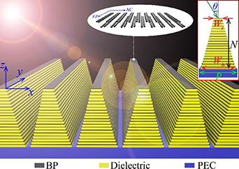
Figure 1. Schematic of the proposed trapezoidal BPMA. Left inset: schematic of monolayer BP; right inset: side view of the proposed structure.
Download figure:
Standard image High-resolution imagewhere j = x, y label the direction concerned, n is the concentration of electrons (chosen as 7 × 1013 cm−2 in this study), and e represents the electron charge, η = 10 meV is the relaxation rate of electrons, mj is the effective mass of electrons along the AC and ZZ directions, and ω is the frequency of incident light. Hence, the equivalent permittivity of BP monolayer can be given as [33]:
where r= 5.76 is the relative permittivity of BP, and 0 is the vacuum permittivity.
According to the EMT, when the thickness of each layer is far less than the incident wavelength, the multilayer structure can be described as a homogeneous medium with an effective anisotropic permittivity (i.e.  ), and the permittivity tensor can be approximately written as:

where p and t represent the in-plane and out-plane permittivity components, and  is the filling ratio of BP in the unit cell. The diagonal elements with different signs (e.g.
  ) will result in a hyperbolic metamaterial. Previously, the trapped rainbow effect was proposed for achieving ultrabroadband absorption using patterned hyperbolic metamaterial taper arrays [23]. The underlying physical mechanism of this effect can be attributed to the slow-light response, which slows down incident waves of different frequencies at different positions within the hyperbolic metamaterial. Therefore, the tapered BPMA is expected to achieve ultrabroadband absorption of incident waves across a wide range of incident angles. Additionally, to evaluate the performance of the absorber, we define an average absorption efficiency (α). Specifically, in the spectral region where absorption efficiency exceeds a threshold value (i.e. we set the threshold at A > 90%), α can be defined as the absorption integrated over the operational bandwidth:
where λ1 and λ2 are the lower and upper limits of the wavelength range.
3. Results and analysis
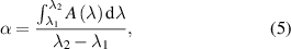
Figure 2(a) illustrates the absorption spectrum of the proposed BPMA for electric field (E) along AC direction under normal incidence. The obtained spectrum exhibits excellent absorption performance with absorptivity exceeding 90% within the range of 25.2–88.8 μm. Clearly, the proposed BPMA exhibits an ultrabroad absorbing band (i.e. 63.6 μm), which is far superior to most BP-based absorbers [38–41, 44, 45]. Additionally, the average absorption efficiency within the absorbing band is 97.8%, indicating that the majority of incident energy can be harvested by the absorber. We further modeled a similar trapezoidal structure made by a homogeneous material with anisotropic permittivity, as shown in the inset of figure 2(a). The absorption obtained from the effective homogenous BPMA (red dashed curve) closely matches that of the actual model (blue solid curve), confirming the applicability of the EMT in our model. Besides, the angular insensitivity of broadband absorption holds significant value in practical applications. The absorption spectra of BPMA at different incident angles are plotted in figure 2(c). It is evident that the broadband absorption feature remains largely unaffected with the increase of θ. Within the wavelength range of 24–74 μm, the absorptivity exceeds 80% even at an incident angle of 60°. In the case of electric field along ZZ direction, the threshold bandwidth reaches 53.6 μm, corresponding to a wavelength range from 41.6 to 95.2 μm. Accordingly, the average absorption efficiency is 97.5% within the bandwidth. Compared with the AC direction, the spectral response in ZZ direction exhibits a narrower bandwidth. Additionally, it is observed that the BPMA has a stable absorption bandwidth for θ up to 30°, while the average absorption efficiency decreases gradually. As θ continuously increases, both absorbance and bandwidth decrease, as shown in figures 2(b) and (d).
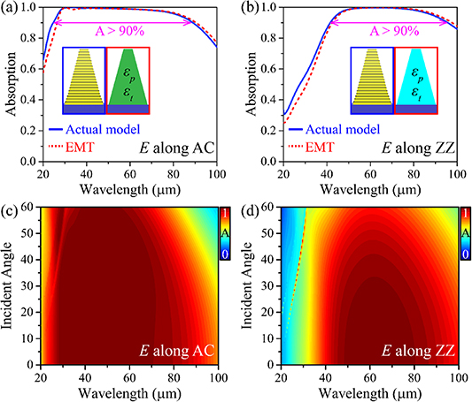
Figure 2. Simulated absorption spectra for the proposed BPMA under normal incidence with the incident electric field E along (a) AC and (b) ZZ directions. (c) and (e) Show the angular dependence of the absorption spectra.
Download figure:
Standard image High-resolution imageTo gain a deeper understanding the process by which incident light is trapped by the BPMA, we examine the normalized magnetic field distributions (|H|) in the BPMA (electric field is along AC direction) at different incident wavelengths. The corresponding magnetic field distributions are also calculated by EMT, as depicted in figure 3. The electromagnetic fields are localized and trapped at different widths of the trapezoidal BPMA, depending on the wavelength. At smaller wavelengths, the electromagnetic field is predominantly concentrated in the upper portion, whereas it gradually shifts towards the lower portion as the wavelength increases. Specifically, when λ = 50 μm, the input energy is primarily harvested in the upper region; at λ = 60 μm, it is localized in the middle region; and at λ = 70 μm, it is predominantly trapped in the lower region. Particularly, unlike the excitation of magnetic polaritons, the magnetic field is not confined in the dielectric layer between adjacent metal layers [46–49], but instead diffuses into several layers. This indicates that the electromagnetic waves can be concentrated in a specific width range and eventually absorbed. The energy flow diagram shown by the blue arrows in figure 3 implies a notable light trapping effect. The incident electromagnetic energy initially propagates downward in the air region and subsequently whirls into the BPMA, generating vortexes at the interface between BPMA and air regions, where it ultimately dissipates. Furthermore, the distributions of magnetic field calculated by the EMT closely resemble the actual model. As the incident wave is coupled into the structure, the group velocity (i.e.  ) of the TM modes at different wavelengths undergoes a significant reduction at their respective critical widths. This phenomenon gives rise to the so-called rainbow trapping effect in the propagation direction.
Figure 3. Distribution profiles of normalized magnetic fields in the cross section of a unit cell in the designed BPMA and its EMT-based counterpart at different incident wavelengths. The blue arrows indicate the energy flow. Herein, the incident electric field is along the AC direction.
Download figure:
Standard image High-resolution imageTo physically explain the fundamental mechanism physically, we conduct a further analysis of the waveguide modes supported in an air/effective BPMA/air planar waveguide. This is achieved by solving the eigen-equation using the EMT as a basis. According to Maxwell's equations and boundary conditions, the dispersion relationship between the incident wave vector ( ) and the propagating constant (
 ) can be expressed as follows:
where  ,
, ![${k_2} = {[{\varepsilon _{\text{t}}}k_0^2 - \left( {{\varepsilon _{\text{t}}}/{\varepsilon _{\text{p}}}} \right){\beta ^2}]^{1/2}}$](https://content.cld.iop.org/journals/2040-8986/26/6/065101/revision2/joptad3ceeieqn11.gif) , and W is the effective core width. By solving equation mentioned above, dispersion curves for different incident wavelengths are plotted in figure 4(a). Obviously, for a given effective core width, the waveguide supports two different propagation constants (solid lines and dotted lines). As the width increases, these two curves intersect at a degeneracy point, denoted by an empty circle. In simpler terms, for waveguide modes with a smaller
, and W is the effective core width. By solving equation mentioned above, dispersion curves for different incident wavelengths are plotted in figure 4(a). Obviously, for a given effective core width, the waveguide supports two different propagation constants (solid lines and dotted lines). As the width increases, these two curves intersect at a degeneracy point, denoted by an empty circle. In simpler terms, for waveguide modes with a smaller  below the degeneracy points (solid lines), the energy flow is parallel to the propagation direction, and these can be classified as forward waveguide modes (i.e.
  ). Conversely, for waveguide modes with a larger
  above degeneracy points (dotted lines), the backward waveguide mode (i.e.
  ) indicates an energy flow anti-parallel to the propagating direction. The existence of degeneracy points suggests a mode conversion between
  mode and
  mode. Interestingly, at the degeneracy point, the energy flow forms a vortex, indicating that both the
  mode and
  mode are trapped in the proposed waveguide structure for a specific core width, as illustrated in figure 3. For different incident wavelengths, the core width of degeneracy point varies and increases with wavelength. The dispersion curves of waveguide modes at W = 5.28, 7.78, and 10.33 μm are shown in figure 4(b). For a waveguide mode, as the electromagnetic wave propagates along the waveguide to a critical width, the group velocity (i.e.
  ) drops to zero, resulting in the wave being captured by the BPMA. When the incident wave vector is small, the propagation constant increases linearly with the incident wave vector, approaching the light line in a vacuum. As the incident electromagnetic wave approaches the degeneracy point, the dispersion curve rises slightly, tending towards flatness. Beyond the degeneracy point, the dispersion curve decreases slightly. Clearly, there is a critical point where the propagating mode has a wave vector close to the cutoff wave vector, corresponding to
  . In other words, for a hyperbolic waveguide with a specific core width, a slow-light mode can be excited in the vicinity of the specific wavelengths. As W increases, the cutoff wave vector decreases, and the corresponding resonant wavelength increases, consistent with the phenomenon observed in figure 3. Taking W = 7.78 μm as an example, we find that when the group velocity is zero, the corresponding
  and
and  are 2.25 × 10⁵ rad m−1 and 1.05 × 10⁵ rad m−1, respectively. Thus, the incident wavelength exciting the slow-light mode is 60 μm. Similarly, the cutoff wavelengths for W = 5.28 μm and 10.33 μm are 50 μm and 70 μm, respectively. Such agreement between the simulation results and theoretical results indicates that the broadband absorption arises from the slow-light effect.

Figure 4. (a) Width-dependent dispersion curves for incident wavelengths λ = 50, 60, and 70 μm. The inset sketches an air/effective BPMA/air waveguide with a fixed W. (b) Dispersion curves of three air/effective BPMA/air waveguides with core widths of W = 5.28, 7.78, and 10.33 μm. The solid lines represent  mode and the dotted lines represent
  mode. Herein, the incident electric field is along the AC direction.
Download figure:
Standard image High-resolution imageNext, we investigate the influence of key parameters on the absorption spectrum. It should be noted that each parameter, such as the top width (Wt), the dielectric layer thickness (h), electron doping of BP (ns ), and the total number of BP/dielectric pairs (N), is varied separately, while leaving other parameters unchanged. As shown in figure 5(a), the overall absorptivity varies slightly in the top width range from 1 to 2.5 μm. As Wt continuously increases, the absorption of the smaller wavelength (near 40 μm) decreases. This is due to the fact that electromagnetic fields at different wavelengths are localized and trapped at different widths of the absorber, and the resonant modes are positively correlated with the width. This means that small wavelengths cannot be effectively absorbed when Wt is increased. Notably, the device still maintains high absorption near the wavelength of 30 μm, which can be attributed to the antireflection effect of the nanocone structure [50]. In figure 5(b), the absorption bandwidth increases with increasing h. This is due to the fact that an increase in height contributes to the energy accumulation and absorption. In figure 5(c), the absorption response is plotted for different electron doping. As ns increases, the absorption spectra are blue-shifted slightly, and the absorbance enhances. The effect of N on the absorption is shown in figure 5(d). When N = 20, the absorptivity can be maintained above 95% across a wide wavelength range. However, for N < 15, the absorptivity of the entire absorption band decreases significantly. The average absorption efficiencies in the wavelength range from 20 to 100 μm are 67.8% (N = 10), 87.8% (N = 15), 94.5% (N = 20), 96.0% (N = 25), and 97.3% (N = 30), respectively. Clearly, as N increases, absorption becomes more efficient and stable. The proposed BP-based far-infrared absorber stands out from previous designs due to its ultra-broadband absorption capability, robust performance at wide angles, enhanced light-matter interaction, and simplified analytical modeling using EMT. These combined advantages make it a highly promising candidate for various BP-based infrared sensing and photodetection applications.
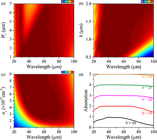
Figure 5. Simulated absorption spectra of the MA with different geometries: (a) varying top width Wt; (b) varying the dielectric layer thickness h; (c) varying the electrical doping of BP; (d) varying the total number of BP/dielectric pairs N. Except as indicated, the geometric parameters are fixed to the default values. Herein, the incident electric field is along the AC direction.
Download figure:
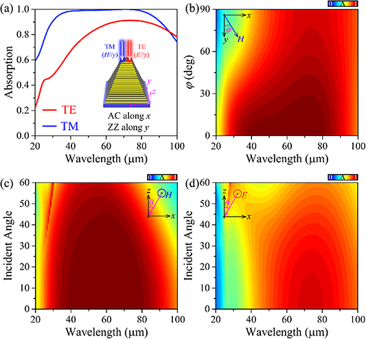
Standard image High-resolution imageInspired by the anisotropic response of the BPMA along AC and ZZ directions, we can construct a 2D periodic array of quadrangular frustum pyramids (AC is along the x-axis), as shown in the inset of figure 6(a). For TM polarization, absorption performance remains excellent, with a bandwidth of 60 μm for absorptivity higher than 90%, corresponding to the wavelength range of 30–90 μm. However, for TE polarization (i.e. electric filed is parallel to y-axis), the overall absorption of the 2D BPMA decreases significantly, with absorptivity higher than 80% occurring in the wavelength range from 50 to 98 μm. Figure 6(b) illustrates the relation between the absorption and the polarization angle (
 ) under normal incidence. As
 increases from 0° (TM) to 90° (TE), both the overall absorbance and bandwidth decrease, resulting in polarization selectivity.
Figure 6. (a) Simulated absorption spectra of 2D quadrangular frustum pyramid arrays under TM and TE-polarized normal incidence. The inset shows the unit cell of the 2D BPMA. The geometric parameters are consistent with that of the structure in figure 2(a). (b) Absorption spectra for different polarization angles from 0° (TM polarization) to 90° (TE polarization) at normal incidence. (c) and (d) Are absorption spectra as functions of incident wavelength and angle of incidence for TM polarization and TE polarization.
Download figure:
Standard image High-resolution image
The tolerance for the wide angles is necessary for the 2D BPMA. We further investigate the absorption effects under oblique incidence. For TM polarization, as shown in figure 6(c), the overall absorption stays larger than 90% within 0° to 47°, and the corresponding bandwidth remains stable from 30 to 90 μm. As θ increases continuously, both the absorbance and bandwidth decrease. Similarly, for TE polarization, as shown in figure 6(d), when θ increases from 0° to 40°, the absorption stays above 80% in the wavelength range from 50 to 98 µm. With a further increase in θ, the absorption gradually decreases. Overall, the 2D BPMA can maintain high and broadband absorption performance over a wide angular range, exhibiting excellent angular stability.
4. Conclusions and perspectives
A far-infrared ultrabroadband trapezoidal BPMA has been proposed to achieve high absorptivity over a wide incident angle. We verified the absorption performance of the BPMA from both theoretical and simulation perspectives. The broadband absorption mechanism is attributed to the slow-light effect. The influence of the key parameters (i.e. top width, dielectric layer thickness, electron doping of BP and the total number of BP/dielectric pairs) are also investigated. Inspired by the anisotropic response of the BPMA, a 2D periodic array of quadrangular frustum pyramids is proposed to achieve polarization dependent broadband absorption. This work has potential applications in BP-based optoelectronic devices, including energy-harvesting materials, thermal emitters, photovoltaic devices, etc.
Acknowledgments
This work was supported by the Research Grants Council of Hong Kong through the Area of Excellence Grant (AoE/P-701/20), the National Natural Science Foundation of China (62305173, 62022001, 12304340), the Natural Science Foundation of the Jiangsu Higher Education Institutions of China (23KJB140015), the Open Project of the State Key Laboratory of Millimeter Waves (K202433), the Natural Science Research Start-up Foundation of Recruiting Talents of Nanjing University of Posts and Telecommunications (NY222080), and Natural Science Research Start-up Foundation of Shanghai University (J07010123209).
Data availability statement
All data that support the findings of this study are included within the article.
Conflict of interest
The authors declare no conflict of interest.