

Abstract
The properties of the guided modes, including the single-mode conditions and the coupling of different polarized modes in the single-crystal lithium niobate photonic wires, were analyzed in detail. One-dimensional photonic crystal micro-cavities with several different patterns, which could be used as an ultra-compact optical filter, were designed and simulated in order to get high transmission at the resonant wavelength and the best preferment. The designed structure, with the whole size of 6.5 × 0.7 μm2, was fabricated on a single-mode photonic wire. A measured peak transmission of 0.34 at 1400 nm, an extinction ratio of 12.5 dB and a Q factor of 156 were obtained. The measured transmission spectrum was basically consistent with the simulation, although a slight shift of resonant wavelength occurred due to the fabrication errors.
Export citation and abstract BibTeX RIS
1. Introduction
Lithium niobate (LN) is a remarkable nonlinear optical material with large second order nonlinear and electric-optical coefficients [1]. Ultra-compact and strong guiding LN photonic wires, which are realized on the single-crystal LN films, have attracted much attention since they enable the ultra-compact photonic integrated devices and high integration density [2]. The ultra-small cross-section of the photonic wire induces higher confinement of light compared with the conventional proton exchange and titanium-diffused LN waveguides [3–5]. This will enhance the performance of many kinds of active optical components, such as wavelength conversion devices [2, 6], tunable LN thin-film ring resonators [7], and waveguide lasers [8].
LN photonic wire is also an excellent platform for making a micro-cavity with small size. Photonic crystal (PC) is an artificial structure that can control the propagation of light through the photonic band gap (PBG) [9, 10]. If a one-dimensional (1D) periodic pattern along the light propagation direction with a defect is embedded into such a system, a compact PC micro-cavity is formed [11]. In the field of telecommunication, such a PC-based cavity can be used as an optical filter for compact photonic devices applied in wavelength division multiplexing (WDM) [12]. The single-mode (SM) condition in the photonic wire should be fulfilled in order to prevent signal distortion during transmission. In addition, the PC micro-cavity provides a platform for studying coherent electron–photon interactions, entangled photon pairs or other quantum optical issues in quantum information processing [13]. Studies of such structures in semiconductors have been extensively reported, particularly in silicon on insulator (SOI) [14]. However, the crystalline inversion symmetry makes the silicon lack the second order susceptibilities, hindering the nonlinear optical applications, such as second harmonic generation, although this problem can be partially solved by inducing a stressing layer [15]. Therefore, the PC micro-cavity based on LN material, is an important integrated optical device that is very promising for enhancing nonlinear-optical effects, which are important to all-optical signal processing. An electro-optically tunable PC cavity on LN film, with polymer benzocyclobutene (BCB) cladding, has also been reported [16]. Compared with BCB cladding, LNOI (lithium niobate on insulator, single-crystal LN films directly bonded to SiO2 on LN substrate) makes higher temperature annealing (as high as 600 °C) possible. This can further eliminate crystal lattice damage induced by ion implantation and allows for the recovery of linear and nonlinear optical properties [17].
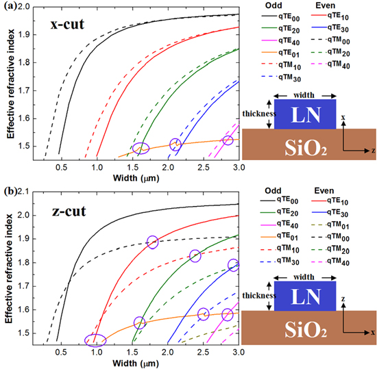
Figure 1. Left: dependence of Neff on the photonic wire width for a (a) x-cut and (b) z-cut 0.69 μm thick LN film. Solid lines and dashed lines corresponded to qTE and qTM modes, respectively. The regions highlighted by purple circles were the mode-coupling regions where the hybrid modes existed. Right: schematic diagrams of a cross-section of the x-cut and z-cut LNOI.
Download figure:
Standard image High-resolution image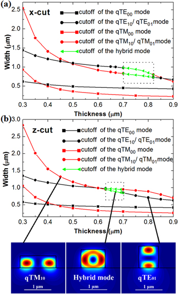
Figure 2. Cut-off dimensions of the first two order modes in the (a) x-cut and (b) z-cut LNOI. The areas between the two curves with the same color (red or black) were the SM regions (for qTM or qTE polarized light). The two green curves were the cut-off of hybrid modes across which the first higher order modes changed from qTE10 and qTM10 to qTM01 and qTE01, respectively. Bottom: Near-field intensity distributions of the modes in the photonic wires with three different dimensions in figure 2(b).
Download figure:
Standard image High-resolution imageIn this paper, we demonstrated an SM LNOI photonic wire fabricated by focused ion beam (FIB) milling. A scanning electronic microscope (SEM) image showed that the maximal width in the cross-section of the photonic wire was 0.7 μm. The effective refractive indices (Neff) of the guided modes with various widths were calculated. Hybrid modes existed if the Neff of the different polarized modes with the same symmetry (even or odd with respect to the symmetrical mirror) had approximate values. The SM condition of both quasi TE (qTE) and quasi TM (qTM) modes in z-cut and x-cut LNOI were obtained by a finite difference eigenmode solver [18]. The simulation results indicated that the 0.7 μm wide photonic wire fabricated in the experiment really fulfilled the SM condition both for qTE and qTM polarized light. An ultra-small (the whole size is 6.5 × 0.7 μm2) 1D PC micro-cavity was fabricated by etching the periodically arrayed holes and leaving a defect in the photonic wire. Several designs of the arrangement of the etched holes were given. The measured peak transmission, extinction ratio and Q factor were 0.34, 12.5 dB and 156, respectively.
2. Simulation
2.1. Characteristics of the guided modes in LNOI photonic wires
Figure 1 shows the Neff of the guiding modes as a function of the width of the photonic wires in z-cut and x-cut LNOI (the thickness was fixed at 0.69 μm, which was the measured value in the experiment) at a wavelength of 1.55 μm. As the dimension of the photonic wire expanded, the Neff increased, and more and more higher order modes existed. qTE00 or qTM00 represented the fundamental qTE or qTM mode. qTE10 or qTM10 represented the first high order qTE or qTM mode with two electric field intensity peaks at the lateral direction and one peak at the vertical direction in the mode profile, while qTE01 or qTM01 represented the first high order qTE or qTM mode with one peak at the lateral direction and two peaks at the vertical direction in the mode profile. We should pay attention to some special regions since they are closely related to some significant applications. If the width was smaller than the starting point of qTE10 or qTM10 (red curves in figure 1) but larger than that of qTE00 or qTM00 (black curves), only one mode for each polarization (qTE or qTM in figure 1) existed. The dimension range for this region (0.3 ∼ 0.86 μm for qTM mode, 0.44 ∼ 0.95 for qTE mode, in z-cut LNOI) was called the SM condition. We looked for such regions for other thickness LN films and the results were summarized in figure 2. The curves represented the minimal dimensions below which the corresponding modes vanished. For example, for a qTE polarized light at 1.55 μm in x-cut sample, if the thickness was 0.5 μm, only the photonic wire with a width larger than 0.49 μm could support qTE00, and when the width increased beyond 1.1 μm, qTE10 existed. Therefore, to fabricate an SM photonic wire based on a 0.5 μm thick LN film, the width should be set between 0.49 and 1.1 μm. A special phenomenon in figure 2 was that the first higher order modes would transit from qTE10 and qTM10 to qTM01 and qTE01, respectively, crossing the hybrid mode (green curves) region. The near-field intensity distribution of qTM10, hybrid mode and qTE01 are shown in the bottom of figure 2 to illustrate the evolution of the first higher mode at the cut-off dimension in a z-cut LNOI. So when the photonic wires were designed in such a dimension range, the polarization of the modes could not be distinguished. Therefore, the smaller value of the two hybrid modes' cut-off dimension (two green curves) should be the upper limit of the SM condition. Other special regions in figure 1 were the mode coupling regions, which were labeled by purple circles. In these regions, it approached the Neff of the two different polarized eigenmodes. As a result, mode coupling occurred between them and the hybrid modes existed. This effect could be used to realize polarization conversion [19]. It should be pointed out that not all the intersections of the two different curves corresponded to the mode-coupling region. Because this structure is symmetrical with respect to the lateral direction, the modes could be classified into even and odd modes. Mode coupling could only occur when the modes had the same symmetry.
2.2. Compact 1D PC micro-cavity
A more complicated optical device based on an SM photonic wire is a 1D PC micro-cavity. The utmost waveguide width with the SM behavior is the optimum condition to realize a filter, because no higher order modes were excited and the fundamental mode had the highest light confinement [12]. Several designs of micro-cavity embedded in PC have been reported, including a single hole removed from the center and the gradually tapered hole arrangements [11, 14]. In this study, we focused on the number and location of the tapered sections in order to find the appropriate one in the system by simulating the transmission spectrum using the 3D finite-difference-time-domain (FDTD) method. The parameters of four different layouts and the corresponding transmissions were illustrated in figure 3. The maximal transmission, extinction ratio and Q factor were important parameters and an ideal filter should have high transmission of the resonant peak, a high extinction ratio and a high Q factor that meant a small full width at half maximum (FWHM) for excellent monochromatic resonant light. In layout a, only a single hole was removed from the center, while in layout b the radii of the two holes on each side of the center decreased to 0.8 and 0.6 times the radii of regular holes, respectively. The 'radius-changed' holes were defined as a tapered section. The tapered section was used to reduce loss resulting from the modal mismatch at the interface between the PC mirrors and the cavity [20, 21]. In layout c, tapered sections were added to the entrance and exit to reduce loss resulting from the mismatch of the guided mode of the photonic wire and the Bloch mode of the PC mirrors. The highest transmission of the resonant light corresponded to layout b, indicating that the tapered section was very effective in coupling the light into and out of the cavity through reducing the modal mismatch between the PC mirrors and the cavity. However, for layout c, the additional tapered section, which was designed to reduce the modal mismatch between the photonic wire and the periodic mirrors, unexpectedly decreased the transmission. This suggested that the additional tapered part was not suitable due to the fact that it might increase the loss induced by the scattering light from the increased number of air holes. An alternative method was to change the regular holes into a tapered shape at the entrance and exit sides as shown in layout d. In this case, an increased resonant transmission was observed, but the extinction ratio was not as large as in that for layout b, especially on the short-wave side of the peak. This would weaken the capability to filter out non-resonant light at the wavelength near the peak. In addition, the FWHM of the transmission peak for layout d was larger than that for layout b, leading to a lower Q factor. After comparing these three factors, layout b was selected to fabricate the PC-based filter. The performances of layouts a, b, c and d, including the maximal transmission of the resonant peak, extinction ratios and Q factors were summarized in table 1. The PC micro-cavity with more holes was also studied. For example, if three regular holes (R = 0.25a) were added on each side of the cavity in layout b and d (the total number of holes would be 20), their Q factors increased to a similar value, about 330. And layout d showed a better transmission (0.06) than layout b (0.02). However, the transmissions of all the layouts greatly decreased with the increased number of holes.

Figure 3. Bottom: different structures of the PC micro-cavity with parameters a = 450 nm, d = 700 nm, and R = 0.25a. Tapered section included two holes with radii of 0.8 and 0.6R respectively. Layout (a): Only a single hole removed from the center. (b): Tapered sections inside the cavity. (c): Additional tapered sections outside the cavity. (d): Tapered section outside the cavity replacing regular air holes. Top: transmission spectra corresponding to the above structures: black line-a, red line-b, green line-c, blue line-d.
Download figure:
Standard image High-resolution imageTable 1. Comparison of three parameters for layout a, b, c, d in simulation.
| Layout | Maximal transmission of resonant peak | Extinction ratio (dB) | Q factor |
|---|---|---|---|
| a | 0.13 at 1355 nm | 28 | 127 |
| b | 0.36 at 1417 nm | 23.7 | 258 |
| c | 0.18 at 1417 nm | 24 | 308 |
| d | 0.62 at 1417 nm | 22.5 | 215 |
The influence of the waveguide width, lattice constant and radius on the transmission profiles was shown in figure 4. First, the impact of the varied widths was illustrated in figure 4(a). The position of the resonant peak and the PBG moved to the long-wave side as the width increased, but the range of the PBG did not change. Second, figure 4(b) showed that a large lattice constant led to a long-wave shift of the resonance peak and PBG. Finally, the influence of the radius on the transmission was shown in figure 4(c). Large radius induced a broadened PBG and a shifted peak towards the short-wave side.

Figure 4. Simulated normalized transmission of the PC micro-cavity with the same pattern in the layout (b) of figure 3 except (a) the width has been changed from 600 to 800 nm, (b) the lattice constant has been changed from 440 to 460 nm, and (c) the radius of the air holes has been changed from 0.23 to 0.27a. These changes corresponded to the possible experimental errors, including a non-rectangular cross-section of the photonic wire, scale errors in the FIB system and the conical shape of the air holes.
Download figure:
Standard image High-resolution image3. Experiment
3.1. Fabrication of the photonic wire and 1D optical filter
LNOI was prepared by crystal ion slicing and wafer bonding methods [2]. A z-cut LN wafer was implanted by He ions and then bonded to SiO2 which was deposited on another LN substrate by plasma-enhanced chemical vapor deposition (PECVD). After annealing, the LN film split from the bulk crystal due to the strain in the damage layer. After polishing, this thin film bonded to SiO2 had a thickness of 690 nm.
To fabricate an SM photonic wire, FIB milling was performed. Since FIB was limited for large-scale milling, the length of the sample was polished to only 0.7 mm at first, and then the etching of the photonic wire was performed. Gallium ions were focused onto the sample with an acceleration voltage of 30 kV. To ensure the quality of the photonic wire and save time simultaneously, first a beam with 13 nA current was used to etch two grooves separated by about 3 μm. Then a 700 pA current beam was used to mill and smooth the sidewalls. Finally, the two end-faces of the photonic wire were smoothed by an ultra-fine beam (120 pA), and a 0.7 μm wide photonic wire was obtained. The cross-section is shown in figure 5(a). Due to the redeposition effect and the expansion of the etching area on the surface, the upper part was narrower than the lower part and a gradient sidewall, of about 7°, was observed. The maximal width in the cross-section was about 0.7 μm.
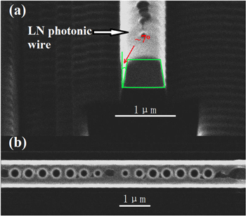
Figure 5. SEM image of (a) the cross-section of the photonic wire and (b) PC micro-cavity with lattice constant a = 450 nm, radius of holes R = 0.25a, and two holes with radii of 0.8 and 0.6R on each side of the cavity. The cross-section exhibits a non-constant width with a sidewall angle of 7° from vertical.
Download figure:
Standard image High-resolution image3.2. Optical characterization
The experimental method and setup of the optical measurement are shown in figure 6. To investigate the transmission properties of the PC micro-cavity, end-face coupling measurement was performed. A tunable semiconductor laser (Santec TSL-210), which was connected by a polarization-maintaining (PM) fiber, was used to emit a beam of linear polarized light. Then the polarized direction was rotated to TE polarization by a positioner. The PM fiber had a lensed tip to improve the mode matching between a waveguide and the fiber. The outgoing light was converged by a 25 × microscope objective, and detected by a germanium photodiode with a resolution of 1 nW.

Figure 6. Optical setup for the transmission measurement of the fabricated sample.
Download figure:
Standard image High-resolution imageThe measured transmission spectrum, having been normalized by a reference photonic wire without air holes, is shown in figure 7. The strong signal variations were Fabry–Perot interference of light reflected from the photonic wire facets and PC mirrors. A maximum transmission of about 0.34 was observed. The Q factor and extinction ratios were 156 and 12.5 dB, respectively. These values were all lower compared with the simulation probably due to transmission loss caused by the rough etched wall and fabrication uncertainties. The measured resonant peak located at 1400 nm, while it located at 1417 nm in the simulation. Thus, a blueshift of about 17 nm of the resonant wavelength existed. Fabrication errors might lead to this discrepancy. A rectified simulation (green curve in figure 7) was performed for the PC micro-cavity with a ladder-shaped cross-section (as in figure 5(a)) instead of a rectangular one. A better agreement of the location of the peak between them was obtained. The original transmission of the photonic wire, including the coupling loss at both ends of the waveguide and the scattering and absorption in the waveguide, was about 0.02 (17 dB), which partly resulted from the mismatch of the fiber mode and the LN waveguide mode. A grating or tapered section could improve the coupling efficiency.

Figure 7. Measured (black line) and simulated (red line) normalized transmission of the PC micro-cavity with the same pattern as figure 5(b). The maximal transmission was about 0.34 and the location of the resonant peak was at 1400 nm. The green curve was the rectified simulated result considering the ladder-shaped cross-section as illustrated in figure 5(a).
Download figure:
Standard image High-resolution image
4. Conclusion
In conclusion, the SM condition and the mode-coupling region in the LN photonic wires were studied based on a full-vectorial finite difference method. Coupling between qTE and qTM modes with the same symmetry with respect to the central mirror would occur if their Neff had similar values. PC-based micro-cavities with several different tapered sections were investigated. An optimal structure, exhibiting a good balance of transmission of the resonant signal, Q factor and extinction ratio was selected. A tapered section enhanced the maximum transmission, however, too many tapered sections, both inside and outside the cavity, might have detrimental effects on filtering out non-resonant light. Experimental fabrication, according to the above simulation parameters, was performed on LNOI by FIB milling. The actual maximum transmission, extinction ratio and Q factor were 0.34 at 1400 nm, 12.5 dB and 156, respectively. The displacement of the location of the resonant peak is attributed to the discrepancy of the parameters between the experiment and the actual design. Research into PC micro-cavities on an LNOI platform offers an important structure and provides guidance for further applications, such as in miniaturized nonlinear-optical enhanced devices and electro-optic modulators.
Acknowledgments
This work is supported by the National Natural Science Foundation of China (Grants No. 11275116, No. 61575111 and No. 11475105).