Abstract
Since the invention of amorphous indium–gallium–zinc–oxide (IGZO) based thin-film transistors (TFTs) by Hideo Hosono in 2004, investigations on the topic of IGZO TFTs have been rapidly expanded thanks to their high electrical performance, large-area uniformity, and low processing temperature. This article reviews the recent progress and major trends in the field of IGZO-based TFTs. After a brief introduction of the history of IGZO and the main advantages of IGZO-based TFTs, an overview of IGZO materials and IGZO-based TFTs is given. In this part, IGZO material electron travelling orbitals and deposition methods are introduced, and the specific device structures and electrical performance are also presented. Afterwards, the recent advances of IGZO-based TFT applications are summarized, including flat panel display drivers, novel sensors, and emerging neuromorphic systems. In particular, the realization of flexible electronic systems is discussed. The last part of this review consists of the conclusions and gives an outlook over the field with a prediction for the future.
Export citation and abstract BibTeX RIS
1. Introduction
Metal oxide semiconductor thin-film transistors (TFTs), especially indium–gallium–zinc–oxide (IGZO)-based TFTs, have received considerable interest since Nomura et al. reported the first amorphous IGZO (a-IGZO) based TFT in 2004. Before the invention of the first a-IGZO-based TFT, the crystalline IGZO materials were first reported as early as 1985[1]. However, it was not until 2003 and 2004 that Nomura et al. used the IGZO materials of single-crystalline and amorphous states as the TFT semiconductor channel materials, respectively[2, 3]. The key advantage of single-crystalline is that there are no defects or grain boundaries, which makes TFTs with ultra-high mobility. However, a high temperature is needed for single crystal growth, which is not favorable for large-area application. In 2004, Nomura et al. reported that a-IGZO film can be deposited at low temperature. Now, a-IGZO films have become the most common TFT channel semiconductor materials. Compared to amorphous silicon TFTs with a field-effect mobility lower than 1.0 cm2/(V·s), a-IGZO-based TFTs usually show a field-effect mobility higher than 10 cm2/(V·s)[4-7].
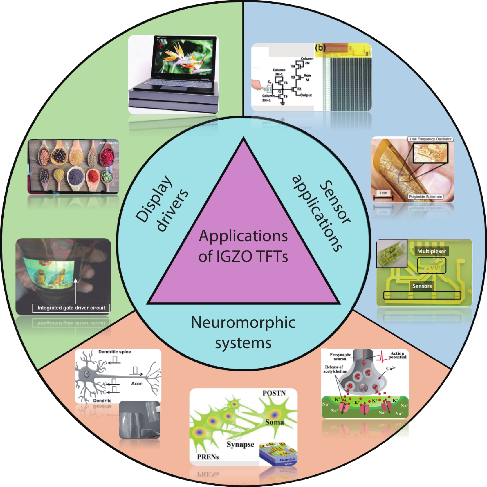
Several well-known display companies (e.g., Sharp, Samsung Electronics, and LG Electronics) have demonstrated that IGZO-based TFTs have many potential applications in liquid crystal displays (LCDs), organic light emitting diodes (OLEDs) display and electronic paper displays[7-14]. In addition to flat panel displays, IGZO-based TFTs are also actively involved in sensor applications and neuromorphic systems. IGZO-based TFTs have the key advantages of distinguishable sensitivities to light, pressure, pH, gas, and some other parameters, which meet the requirements of these sensors. Furthermore, based on the relatively mature display technology, sensors with IGZO-based TFTs are easier to manufacture[15-30]. In particular, the IGZO-based TFTs show great potential in the field of flexible electronics because of their unique advantages of light-weight, ultrathin thickness and resistance to mechanical bending[13, 31-33]. IGZO-based TFTs with electrolyte gate dielectrics are very favorable for artificial synapse/neuron emulation, due to the interfacial electric-double-layer coupling and electrochemical doping effects[34-41]. IGZO-based TFTs neuromorphic devices show very low-energy consumption down to pJ/spike because of the extremely high gate capacitance of the electrolyte gate dielectrics and the high resistance of IGZO channel layers[42-45]. Some important applications of IGZO-based TFTs are shown in Fig. 1.
Download figure:
Standard imageWith the rapid development of IGZO-based TFTs in various aspects of our life, especially in the field of display, a large number of studies based on the IGZO-based TFTs have been reported. Thus, this article aims to review the recent progress and the major trends in the field of IGZO-based TFTs. In this paper, we review the materials, devices and applications of IGZO-based TFTs. First, the history, electron travelling orbitals and deposition methods of the IGZO thin film are introduced. Second, we introduce the traditional devices and the new-concept device structures. Third, we comprehensively discuss the main applications, including display drivers, sensor applications and neuromorphic systems using IGZO-based TFTs. Finally, our conclusions and the outlook for IGZO-based TFTs are discussed.
2. IGZO materials and TFTs
2.1. IGZO materials
Crystalline IGZO materials were first discovered by Kimizuka et al. in 1985[1]. These authors successfully fabricated InGaZnO4 with YbFe2O4-type structure by sintering at a temperature above 1000 °C. Until 2003 and 2004, the single-crystalline and amorphous state IGZO materials were proposed for TFT channel semiconductors by Nomura et al.[2, 3], respectively. In 2003, Nomura et al. presented a transparent TFT with single-crystalline IGZO thin film as the channel layer. The unique advantages of the single-crystalline InGaO3(ZnO)5 thin film are that there are no grain boundaries and defects, which enable the single-crystalline IGZO-based TFT to show a field-effect mobility (μFE) as high as ~80 cm2/(V·s). However, a high annealing temperature of 1400 °C was needed to form the single-crystalline phase. This high temperature process limited the practical application. In the next year, amorphous IGZO (a-IGZO) thin films were deposited at low temperature by Nomura et al.[3]. This a-IGZO thin film was prepared by pulsed laser deposition (PLD) using a polycrystalline InGaZnO4 ceramic target. The first a-IGZO-based TFT showed a saturation mobility of 6–9 cm2/(V·s), a current on/off ratio (Ion/Ioff) of 103 and threshold voltage (Vth) of 1.6 V.
The electron travelling orbitals of oxide semiconductors are different from covalent semiconductors. Covalent semiconductors (e.g., silicon) possess carrier transport paths of directive sp3 orbitals[3]. Thus, the electron mobility of single crystal silicon can reach up to 1000 cm2/(V·s)[38]. However, if the carrier conducting pathway was disrupted in the case that the crystalline structure was broken or under amorphous state, then the carrier mobility would be lower by three orders of magnitude than single crystal silicon[39]. Unlike covalent semiconductors, oxide semiconductors are of degenerate band conduction. Fig. 2 shows the carrier transport paths of crystalline and amorphous oxide semiconductors. The carrier transport paths of metal oxide semiconductors are composed of spatial metal ns orbitals with isotropic shape. Because s orbital is of spherical symmetric, the overlap in distorted metal–oxygen–metal can also offer a conductor pathway.

Fig. 2 (Color online) Carrier transport paths of (a) crystalline, (b) amorphous post-transition-metal oxide semiconductors[3].
Download figure:
Standard imageMany methods have been proposed to deposit IGZO thin films. The most commonly used method is sputtering because it is compatible with uniform deposition on the large surface with low cost[40, 41, 49]. Pulsed laser deposition (PLD)[3], atomic layer deposition(ALD)[50-52], plasma enhanced chemical vapor deposition (PECVD)[53-55] and solution methods such as spin-coating, inkjet printing and gravure printing[56] are also used for IGZO-based TFT fabrication. These methods possess unique advantages, for example, IGZO thin film grown by ALD showed a roughness at the atomic level. The PECVD method can well control the reactive species concentration and further regulate the film deposition rate.
2.2. IGZO-based TFTs
The first concept of thin-film transistors (TFTs) was patented as early as the 1930s[57]. However, TFTs were only at the concept stage without vacuum technology and an understanding of semiconductors. The first practical TFT was fabricated in 1962 by Weimer[58]. In his experiment, microcrystalline cadmium sulfide film was used as the semiconducting channel layer and silicon oxide was used as the gate dielectric. Since 2003, zinc oxide (ZnO) TFTs have attracted much interest[59-61]. However, ZnO films crystallize at low temperature and usually show polycrystalline structure, which is not suitable for large-area macroelectronics. Fortunately, Nomura et al. invented the first a-IGZO-based TFT in 2004[3]. IGZO-based TFTs have gradually gained practical applications thanks to their high electrical performance, large-area uniformity, and low processing temperature. Fig. 3 shows a time axis diagram of the development of the IGZO-based TFTs.

Fig. 3 (Color online) A time axis diagram of the development of the IGZO-based TFT[1–3, 11, 20, 36, 44, 57, 62].
Download figure:
Standard imageMany possible device structures for IGZO-based TFTs are shown in Fig. 4 [63, 64]. Figs. 4(a)–4(e) show the bottom-gate structure, top-gate structure, dual-gate structure, vertical structure and multiple gate structure, respectively. Figs. 4(a) and 4(b) are the simplest device structures that require very few manufacturing steps, which are very friendly to the laboratory device preparation. For example, the structure in Fig. 4(a) just needs one lithographic step, which makes the device preparation relatively quick and cheap. However, the electrical properties of those devices are unstable because the channel materials are exposed to the atmosphere, and will be influenced by the moisture and oxygen in the air. In the dual-gate structure, just as the name implies, bottom gate and top gate are together used to control the device properties, such as the threshold voltage, subthreshold swing, current on/off ratio[65-68]. The devices of vertical structure possess small footprint, resistance to the bending stress and controllable channel length[69-71]. TFTs of multiple in-plane gate electrodes are used in neuro-transistors to simulate spatiotemporal information processing[72].

Fig. 4 (Color online) Schematic diagrams of the device structures with (a) bottom gate, (b) top gate, (c) double gate, (d) vertical and (e) multiple gates.
Download figure:
Standard imageIn IGZO-based TFTs, source/drain electrodes, gate electrode, gate dielectric and IGZO semiconductor channel material are used in the TFT structures. Electrodes are usually composed of metal materials, high conductive metal oxides and new materials such as graphene[70, 73, 74]. Various materials are used as gate dielectrics. First, traditional gate dielectrics like SiO2 and SiOx [66, 75], which can be compatible with traditional TFT fabrication process. Second, high κ materials, such as Al2O3, HfO2, ZrO2, Y2O3 and Ta2O5 [50, 70, 76]. The advantages of these materials are that they can reduce the equivalent oxide thickness and decrease the device size. However, they are of poor interface quality and reduce compatibility with the TFT fabrication process. Third, organic gate dielectrics such as olefin polymers and polyvinyl pyrrolidone (PVP)[77, 78]. These organic gate dielectrics are usually used in the flexible electrics. Finally, ion gate dielectrics, such as proton conducting nanogranular SiO2 and chitosan[79, 80]. These dielectrics are actively used in the electric-double-layer TFTs and produce a large capacitance.
Sato et al. presented a bottom-gate type coplanar homojunction a-IGZO-based TFT[75]. In this work, they employed highly doped contact regions naturally formed by depositing upper protection layers made of hydrogenated silicon nitride. As a result, a nearly ideal Ohmic contact was formed with a low parasitic source-to-drain resistance of 34 Ω·cm. Fig. 5(a) shows a schematic diagram of the TFT structure. The device was fabricated on a glass substrate. The molybdenum (Mo) layer was sputtered as the bottom-gate electrode. The SiOx layer was deposited by PECVD as the gate dielectric. This gate dielectric material is commonly used because it is compatible with the traditional TFT fabrication process. Then, the a-IGZO semiconductor film was deposited by direct-current magnetron sputtering and used as channel layer at room temperature. SiOx /SiNx layer was deposited by PECVD and used as a protection layer. The region that was not covered SiOx after depositing SiOx /SiNx film was converted to highly conductive source/drain electrodes. Figs. 5(b) and 5(c) show the transfer and output curves of the TFTs, respectively. The device showed a good subthreshold swing (SS) of 0.13 V/decade, a Vth of 0.13 V, and an Ion/Ioff of over 109 at Vds = 10 V. From the output characteristics, we can see a steep rise in the low Vds region, which indicated a good Ohmic contact between semiconductive a-IGZO and source/drain electrode.
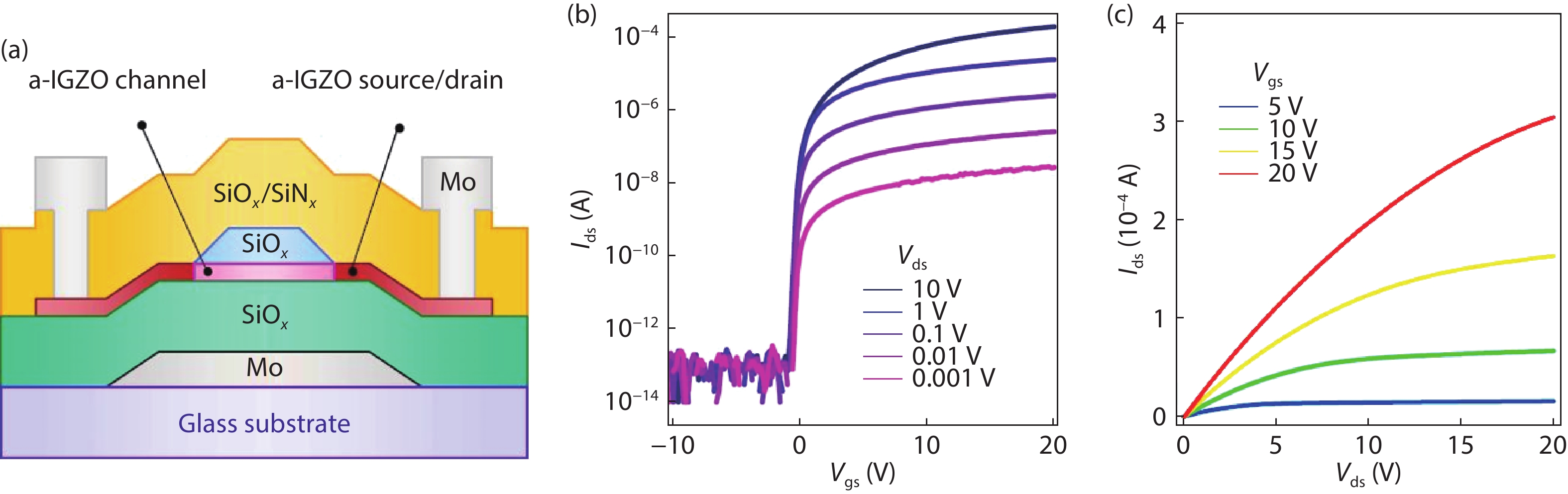
Fig. 5 (Color online) (a) Schematic diagram of the bottom-gate coplanar homojunction a-IGZO device structure. (b, c) Transfer and output curves of the device, respectively[75].
Download figure:
Standard imageZhang et al. proposed a self-aligned top-gate a-IGZO-based TFT with a thickness of 8.62 nm SiO2 as gate dielectric[74]. This device realized the ultrathin gate dielectric less than 10 nm with low leakage current. Fig. 6(a) shows the structure of the TFT and the major processing steps, respectively. A thickness of 40 nm a-IGZO thin film was deposited on the glass substrate by sputtering at room temperature. A thin SiO2 film with thickness lower than 10 nm was deposited as the gate dielectric by PECVD at 300 °C. The 80 nm thick Mo film was then deposited on the SiO2 layer and patterned to form the gate electrode by dry etching. Finally, the Mo layer was used as the source/drain electrodes by a lift-off process. Figs. 6(b) and 6(c) show the transfer and output characteristics of the a-IGZO-based TFT, respectively. The a-IGZO-based TFT showed a low off-state current of less than 10–12 A, a low gate leakage current of 10–13 A, a μFE of 10.13 cm2/(V·s), a Vth of 0.52 V and a high Ion/Ioff over 108 at Vds = 2.1 V. Such a-IGZO TFTs with ultrathin SiO2 gate dielectric have achieved a low gate leakage current and have also shown a good electrical stability under positive and negative gate bias stresses.

Fig. 6 (Color online) (a) Schematic diagram of the top-gate a-IGZO-based TFT structure and the major processing steps, respectively. (c, d) Transfer and output curves of the a-IGZO-based TFT, respectively[74].
Download figure:
Standard imageIn the dual-gate structure, the top gate and bottom gate are together used to modulate the channel carrier concentration and further control the electrical performance of the device, such as the turn-on voltage, the threshold voltage and the field-effect mobility, through applying voltage to the bottom and top-gate electrodes[81-84]. The work principle of dual-gate TFT is somewhat like that of the single-gate TFT, utilizing the electric field capacitively to control the channel. By changing the polarity or amplitude of the voltage applied to the bottom or the top gate, the channel actually becomes enhanced or depleted. The concentration of the conductive carriers (the majority carriers) changes and the electrical performance of the device can also be modulated. Li et al. presented a comparison between the single-gate and dual-gate TFTs[66]. Figs. 7(a) and 7(b) show the schematic structures of the single-gate and dual-gate devices, respectively. The a-IGZO thin film was deposited as the channel layer by reactive sputtering. Figs. 7(c) and 7(d) show the transfer and output curves of the single-gate TFT, respectively. Figs. 7(e) and 7(f) show the transfer and output curves of the dual-gate TFT, respectively. Compared with the single-gate TFT, the performance of the dual-gate TFT is more superior. The on current was 2.54 times higher than that of the single-gate TFT, the μFE was about 1.23 times higher than that of the single-gate TFT, and SS was about half of the single-gate TFT.
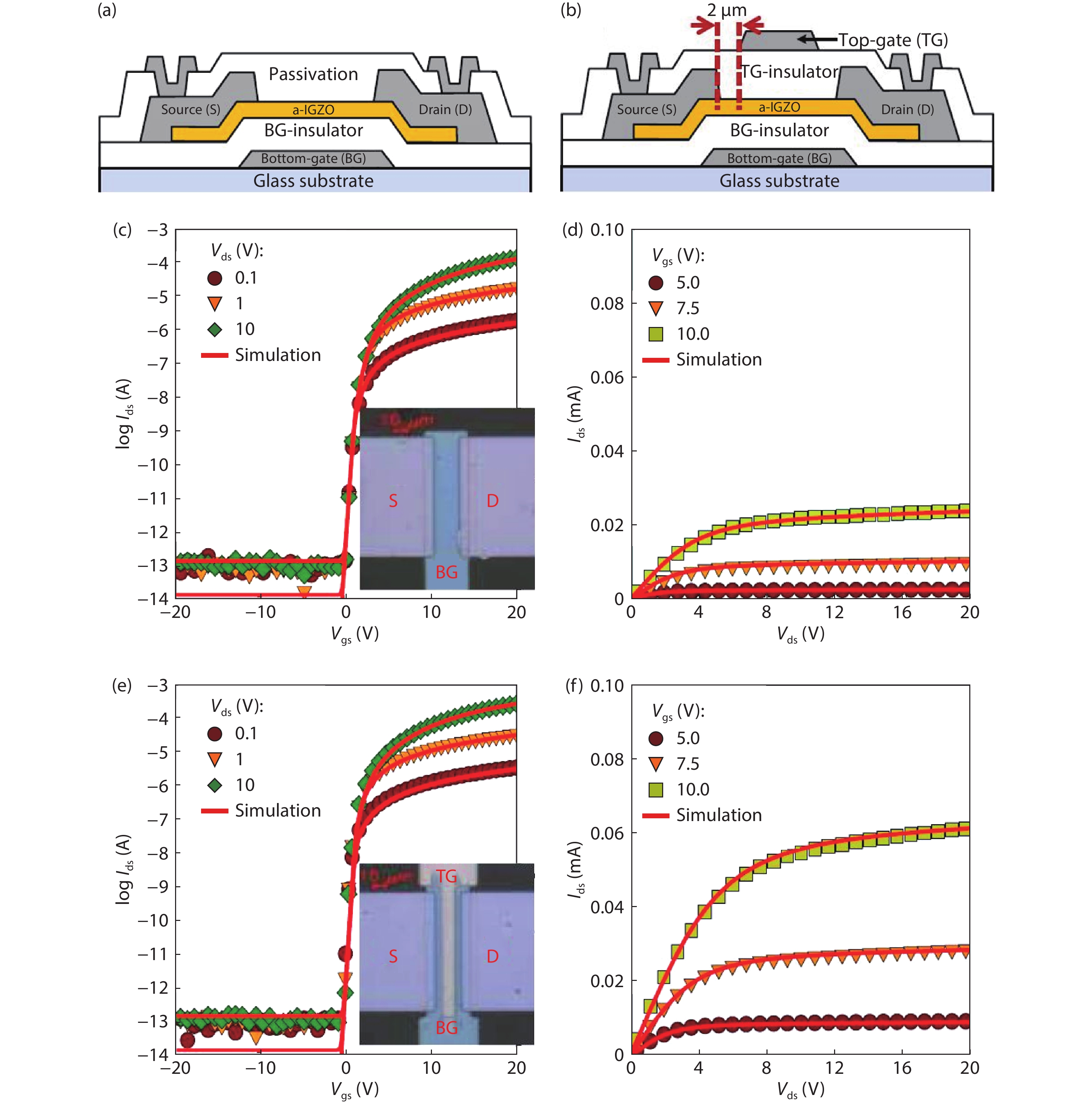
Fig. 7 (Color online) Schematic diagrams of the structures of (a) single-gate and (b) dual-gate TFT, respectively. (c, d) Transfer and output curves of the single-gate device, respectively. (e, f) Transfer and output curves of the dual-gate device, respectively[66].
Download figure:
Standard imageVertical structure devices can offer ultrashort channel with high current. Furthermore, the ultrashort channel enables the device to resist mechanical stress, which is especially important for flexible devices[70]. In planar IGZO-based TFTs, a few cracks in the IGZO thin film can severely degrade the migration of the carriers. However, in vertical structures, the vertical current is unaffected by planar cracks. When the device suffers an external mechanical stress, usually causing several cracks across the IGZO thin film, as shown in Fig. 8(d), the TFTs in the vertical structure are less affected because the current transfer between the source and drain is in the vertical direction. Liu et al. presented a highly flexible vertical TFT with the IGZO thin film as the channel layer[70]. Fig. 8 shows the vertical device structure and the charge transport paths in the planar and vertical TFTs, respectively. The structure of the vertical TFTs is based on the vertical heterostructure of graphene-IGZO-metal stack. Tanium (Ti) was sputtered as the drain electrode. The IGZO thin film was deposited as the channel layer. The chemical vapor deposition (CVD) graphene was transferred onto the IGZO thin film as the source electrode. A thickness of 40 nm Al2O3 thin film was deposited on the top of the channel as the gate dielectric with high dielectric constant. When the cracks appeared in the IGZO thin film, as shown in Figs. 8(c) and 8(d), the carriers cannot be transported in the planar structure because the source/drain electrodes are both in the same plane and the current is blocked by the cracks. However, as shown in Figs. 8(a) and 8(b), the source/drain electrode and gate electrode are in the vertical direction, and thus the carrier transfer are less affected. Based on the characteristics of the resistance to mechanical stress, these vertical structure TFTs are significantly favorable for the application of flexible electronics.
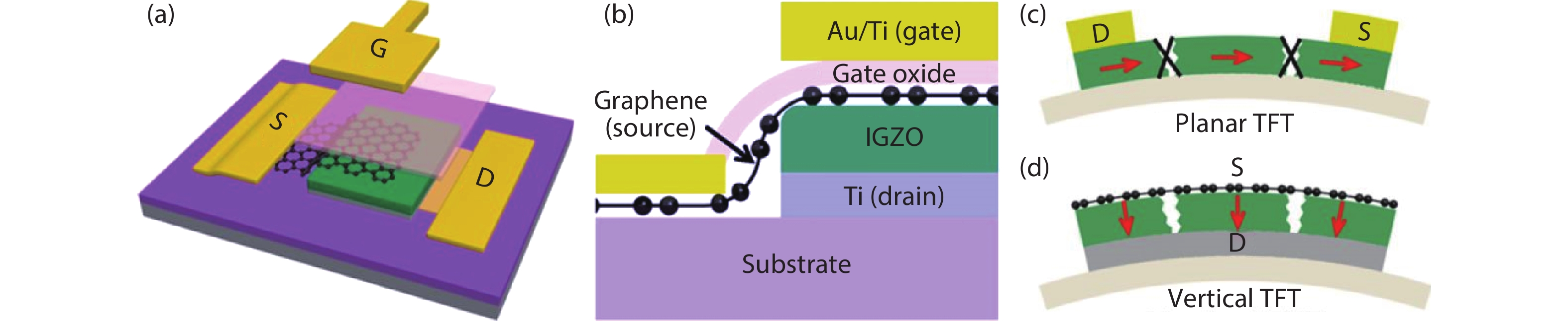
Fig. 8 (Color online) (a, b) Schematic diagrams of the vertical IGZO-based TFT structures. (c, d) Carriers transferred in the planar and vertical TFTs with cracks in the IGZO thin film, respectively[70].
Download figure:
Standard imageIn 2017, IGZO-based neuron TFTs with multiple in-plane gate electrodes were reported by our group[72]. Fig. 9 shows the device structure of the neuron TFTs gated by a nanogranular SiO2 electrolyte film. Electric-double-layer effect due to the mobile proton in the SiO2 electrolyte film provided a very large specific gate capacitance. Voltage pulses applied on the in-plane gate electrodes can be temporally and spatially coupled to the IGZO channel layer due to the indium–zinc–oxide (IZO) floating gate. These IGZO-based neuron TFTs are favorable for sensors and neuromorphic applications.

Fig. 9 (Color online) Schematic diagram of the IGZO-based neuron TFTs with multi-gate structure[72].
Download figure:
Standard image3. Applications
IGZO-based TFTs have been applied in many areas, such as display drivers, sensors and neuromorphic systems[10, 23, 25, 85-88]. In this section, we will introduce the important applications based on IGZO-based TFTs in commercial production and scientific research.
3.1. Display drivers
Hydrogenated amorphous silicon (a-Si:H) and low-temperature polysilicon (LTPS) have been widely used in practical displays. However, the electron mobility of a-Si:H is usually low (1.0 cm2/(V·s)) and the TFTs are unstable under stress and illumination[4]. LTPS TFTs possess high mobility and good stability compared to a-Si:H TFTs[11]. Nevertheless, the process cost of preparing LTPS films is relatively high, especially for large-size displays[4, 5, 85, 89]. In addition to these two materials, the IGZO thin film has the advantages of high electron mobility, low-temperature fabrication process, high uniformity of large area and low cost. These advantages ensure that the IGZO-based TFTs are favorable for the applications of displays[9, 11-13, 31, 41, 85, 90-103].
3.1.1. LCDs
LCDs are a relatively mature technology and are used in display panels, such as smart phone displays, tablet personal computers and televisions. The trends of LCDs are high resolution (7680 × 4320 pixels), ultra-high pixel density of over 300-ppi (pixels per inch) and refresh rate of 240 Hz or higher. To follow these trends, smaller and faster TFTs are required. Consequently, a-IGZO-based TFTs are considered as an advanced method to achieve the high pixel density on a large panel size, due to their high mobility and small size. For example, Baek et al. reported a dual-gate synchronized a-IGZO-based TFT for the application of an active-matrix liquid crystal display (AMLCD)[91]. To understand the operation principle of the dual-gate a-IGZO-based TFT under synchronized bias conditions, a mathematical analysis of the dual-gate synchronized a-IGZO-based TFT is analyzed in this work. The equation of current in saturation region is IDS = WμC(VGS – VTH)2/2L, and the equation of subthreshold swing is SS = (∂ log10 IDS/∂ VGS)–1, where W and L are the channel width and length, C is the capacitance of the channel semiconductor, and μ is field-effect mobility. Compared with the top-gate, bottom-gate, and synchronized dual-gate a-IGZO TFTs only by bias conditions, from the calculations, the dual-gate a-IGZO-based TFTs under synchronized bias produced larger current and steeper SS compared to the single-gate TFTs with the same channel width/length ratio. These superior properties of the a-IGZO-based TFTs allow the AMLCD to have high pixel density and high resolution. Fig. 10 shows the proposed pixel circuit with the synchronized dual-gate a-IGZO-based TFT for the AMLCD. In the pixel, the switching transistor (a-IGZO-based TFT) was of an inverted staggered structure with an additional gate electrode (top gate). Furthermore, the top gate and the bottom gate were tied together through the sync via, which prevented the dual-gate TFTs from suffering the degradations of the mobility and subthreshold swing. These a-IGZO-based TFTs achieved a smaller size for the same amplitude of drain current.
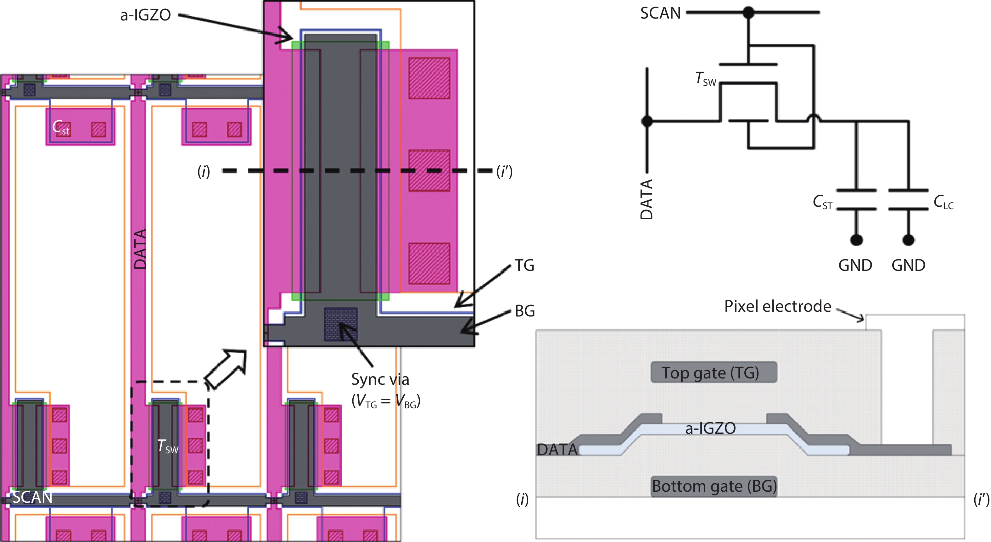
Fig. 10 (Color online) Pixel circuit of the AMLCD based on synchronized dual-gate a-IGZO-based TFTs[91].
Download figure:
Standard image3.1.2. OLEDs
OLEDs driven by a-IGZO-based TFTs are still in the development stage and they have not been put into the display market on a large scale. For further development, crucial problems such as device stability, imaging uniformity and yield[104-108] need to be solved urgently. For example, the threshold voltage of the a-IGZO-based TFT usually shifts under electrical bias stress[108], which would cause non-uniform brightness in the OLED displays. Fortunately, TFTs with dual-gate structure can control the threshold voltage with little variation[101]. Wang et al. reported a dual-gate a-IGZO-based TFT-driven pixel circuit for active-matrix OLEDs (AMOLEDs)[101]. Figs. 11(a) and 11(b) show schematic diagram and the electrode definition of the dual-gate TFT structure, respectively. The bottom gate and the top gate were defined as the primary gate and the auxiliary gate, respectively. The threshold voltage of the dual-gate TFT under the primary gate operation can be modulated by the auxiliary gate voltage. Fig. 11(c) shows the transfer curves of the dual-gate a-IGZO-based TFTs under the primary gate operation with auxiliary gate voltage changing from –4 to 4 V. As shown in Fig. 11(d), the threshold voltage shifted linearly with the auxiliary gate voltage. Therefore, the Vth variation under the primary gate operation could be compensated by varying auxiliary gate voltage. Fig. 11(e) shows a schematic of the pixel circuit including one driving TFT (T1), four switching TFTs (T2–T5) and two capacitors (C1 and C2).

Fig. 11 (Color online) (a) Schematic diagram of the measured dual-gate a-IGZO-based TFT structure. (b) Definition of the electrodes. (c) Transfer curves of the dual-gate a-IGZO-based TFT under primary gate operation with auxiliary gate voltage changing from –4 to 4 V. (d) Threshold voltage as a function of auxiliary gate voltage. (e) Structure of the pixel circuit[101].
Download figure:
Standard image3.1.3. Flexible displays
Flexible IGZO-based TFTs are capable for use as flexible displays, due to the unique advantages such as light-weight substrates[87, 109-112], low-voltage-driven[113], and bendability[114, 115]. In addition, when the IGZO thin films are deposited on to suitable substrates, the IGZO-based TFTs can be used to form fully transparent flexible displays. Flexible displays driven by IGZO-based TFTs have been researched in many works[13, 31, 34, 116]. For example, in 2009, Park et al. fabricated a 6.5 inch full-color flexible AMOLED on the polyimide (PI) substrate driven by a-IGZO-based TFTs[13]. The a-IGZO-based TFT showed a Vth of 0.9 V, an SS of 0.25 V/dec, a μFE of 15.1 cm2/(V·s). Moreover, there was no performance degradation under bending of the R = 3 mm. Nag et al. presented a top-emitting quarter-quarter-video-graphics-array AMOLED display with 85-ppi resolution driven by a-IGZO-based TFTs[31]. In this display panel, the driven a-IGZO-based TFT showed high electronic characteristics of μFE of 12.0 cm2/(V·s), SS of 0.5 V/dec, and Ion/Ioff of over 107.
Most TFT gate drivers integrated on the display panel use carry signals between the stages. However, in the flexible display the error of the stressed stages is accumulated through the carry signals when the display panel is bent. This problem will probably lead to the failure of the image refresh. To deal with this problem, Kim et al. reported a carry-free gate driver for flexible displays using a-IGZO-based TFTs[117]. This carry-free gate driver overcame that problem because it did not use the carry signals and each unit stage operated independently. Fig. 12(a) shows the conceptual architecture and the output waveforms of the carry-free gate driver. Each unit stage works as a decoder and the output of each stage is decided by the binary-weighted decoder signals. When the mechanical stress is applied, the outputs of the stressed stages would become slower but the errors could not accumulate because there are no carry signals through which the error can propagate and each stage works independently. As shown in Fig. 12(b), the flexible display with a carry-free gate driver can keep the normal operation, even under the mechanical stress. Moreover, the carry-free gate driver showed no voltage fluctuation at the outputs after 10 000 cycles bending test with a bending radius of 2 mm. These carry-free gate drivers achieve high reliability under mechanical stress compared with the traditional carry-type gate drivers for flexible displays.

Fig. 12 (Color online) Conceptual architecture and flexible display panel with carry-free gate driver[117].
Download figure:
Standard imageTable 1 shows the recent studies of the display applications driven by the a-IGZO-based TFTs. This table shows the substrate, structure, electrical properties of the a-IGZO-based TFTs, the size of the display panel and the specific application.
Table 1. Display applications of the IGZO-based TFTs.
| Substrate | Structure of the TFT | μFE(cm2/(V·s)) | Vth(V) | SS (V/dec) | Size (inch) | Application | Ref. |
|---|---|---|---|---|---|---|---|
| Glass | Dual-gate | 11 | 0.24 | 130 | 55 | LCD | [118] |
| Glass | Inverted stagger | 9 | — | — | 32 | LCD | [48] |
| Glass | Bottom gate | 15 | 3.2 | 0.4 | 80 | LCD | [104] |
| Glass | Inverted bottom gate | 4.2±0.4 | –1.3 | 0.96±0.1 | 15 | AMLCD | [12] |
| Glass | Back channel etch | 7.35 | 1.6 | — | — | AMLED | [100] |
| Glass | Staggered bottom gate | 8.2 | 1.1 | 0.58 | 12.1 | AMOLED | [11] |
| — | — | 18.45 | 1.04 | 0.73 | — | AMOLED | [97] |
| Glass | Etch stopper | 20 | — | — | 4.8 | AMOLED | [103] |
| Polyimide | Staggered bottom gate | 17.3 | 0.86 | 0.21 | 11.7 | Flexible AMOLED | [119] |
| Polyimide | Inverted staggered bottom gate | 11.6 | 1.6 | 0.25 | 3 | Flexible AMOLED | [34] |
| Polyimide | Coplanar | 10.25 | 0.34 | 0.22 | — | Flexible OLED | [120] |
Nowadays, a-IGZO-based TFTs have attracted considerable attention thanks to their large-size, high-resolution and narrow-bezel display applications. Fig. 13 shows this progress in display applications. For example, China Star Optoelectronics Technology (CSOT) developed an 85-inch 8k4k LCD driven by the IGZO-based TFTs. The large-size LCD panel is shown in Fig. 13(a) [121]. Fig. 13(b) shows a 1058-ppi ultra-high-resolution flexible OLED display using IGZO-based TFTs fabricated by Semiconductor Energy Laboratory[62]. Usually, in the display market, displays with a pixel of about 400-ppi are used. This OLED display showed an ultra-high resolution of 1058-ppi with c-axis-aligned nanocrystalline IGZO materials and could be used for mass production. LG Display demonstrated a bezel free designed AMOLED driven by a-IGZO-based TFTs in 2019[122]. Fig. 13(c) shows an image of the panel. In the fabrication process, this panel is designed to be bezel free. The small remaining bezel of 0.x mm is shown in Fig. 13(c), due to the panel cutting process from the mother glass. We believe that in the future displays driven by the IGZO-based TFTs will gradually occupy a dominant position not only in the field of LCD or OELD but also in the field of true flexible displays.
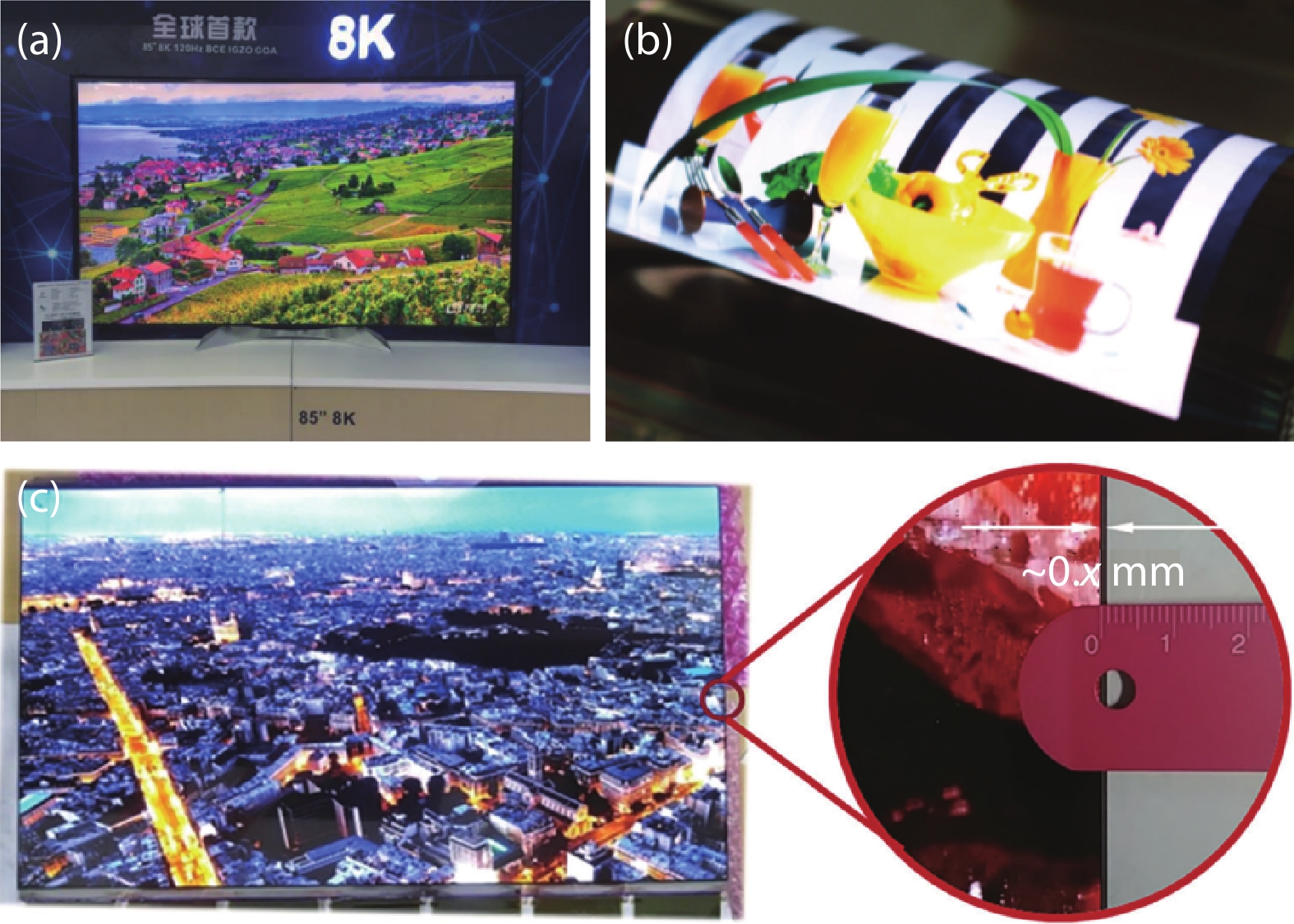
Fig. 13 (Color online) Picture images of the display panels of large size, high-resolution and narrow bezel[62, 121, 122].
Download figure:
Standard image3.2. Sensor applications
Sensors can detect the light, force, voice, gas, humidity et al. and transfer them into electrical signal. At present, sensors have been applied in industrial manufacture, healthcare monitoring[123], food safety[124], artificial electronic skins and so on. IGZO-based TFTs are compatible with semiconductor integrated circuit technology and they possess the advantages of small size, room-temperature fabrication process and sensitivity to the pH, pressure, light, gas and so on[16, 20, 22, 23, 25, 125-128], which meet with the requirements of the sensors. In this section, we will present the main sensor applications based on the IGZO-based TFTs.
3.2.1. Photodetectors
Photodetectors have attracted increasing attention, due to their wide applications in biomedicine, fire monitoring, photo-communication, missile plume detection and so on. The photodetectors based on the IGZO-based TFTs exhibit a relatively high response to light with a wavelength lower than 420 nm because the IGZO materials possess a wide bandgap over 3.0 eV. For example, Yu et al. presented an ultraviolet (UV) photodetector based on the IGZO-based TFT with a p–n junction[27]. Fig. 14 shows a schematic diagram of the IGZO-based TFT structure, the carrier transmission process under the light and the photo responsivity of the IGZO and PEDOT:PSS/SnOx /IGZO TFTs, respectively. The p–n junction was composed of the PEDOT:PSS/SnOx /IGZO heterojunction structure. Through the p–n junction, the directional carrier transfer of the photo-generated carriers was experimentally validated. A photo responsivity of 984 A/W at a wavelength of 320 nm was obtained in this work. This work has successfully fabricated a visible-blind ultraviolet photodetector based on the a-IGZO TFTs and achieved ultra-low-power dissipation of lower than 10 nW under illumination and about 0.2 pW in the dark. Moreover, this photodetector with high photoresponsivity has the unique advantage of pixel integration, which can potentially be applied in high performance visible-blind ultraviolet photodetector pixel arrays. Besides the UV photoelectric sensors, the IGZO-based TFTs with narrow-bandgap materials such as graphene dots[129], silver nanoparticles[130] and polymer[131] have successfully been used in visible-light photoelectric sensors. For example, in 2010, Zan et al. demonstrated a visible-light phototransistor that consisted of a wide-bandgap a-IGZO and a narrow-bandgap (about 2 V) poly (3-hexylthiophene) (P3HT)[131]. The a-IGZO thin film and P3HT formed a p–n junction diode. The P3HT layer has a high absorption coefficient for visible light and absolutely absorbs visible light, and consequently injects electrons into the a-IGZO layer. As a result, the concentration of the carriers in the channel and also the threshold voltage of the a-IGZO-based TFT change rapidly with the illumination. In this work, the authors proposed a simple way to convert a wide-bandgap a-IGZO-based TFT into a visible-light photodetector that has a fast response and a high sensitivity. Although ultraviolet and visible-light phototransistors have been fabricated in many works, there are few reports of infrared photodetectors based on IGZO TFTs. Lee et al. for the first time characterized the infrared photoresponse principle through the subgap density-of-states over the forbidden bandgap of a-IGZO[26]. The origin of the sub-bandgap (hν < Eg) photo response in a-IGZO-based TFTs was that the electrons were optically pumped from the photo-responsive sub-bandgap states. From these works, we can see that the photodetectors based on the IGZO-based TFTs have been investigated from ultraviolet to infrared. These works provide useful results that can help the integration of the photodetectors based on the IGZO-based TFTs.

Fig. 14 (Color online) (a) A schematic diagram of the IGZO-based TFT structure. (b) The separation and collection process of the photo-generated carriers. (c) Photoresponse of the IGZO and PEDOT:PSS/SnOx /IGZO phototransistors as a function of the light wavelength[27].
Download figure:
Standard image3.2.2. Pressure sensors
Pressure sensors are used to monitor pressure magnitude and fluctuation, which are important in areas such as blood flow, heartbeat, and respiratory system of the human body[132]. Piezoelectric sensors have attracted much attention because they can generate an electric potential in response to an applied pressure. Geng et al. proposed a pressure sensor based on a dual-gate a-IGZO-based TFT with a polyvinylidene fluoride (PVDF) piezo-capacitor[133]. When the pressure is applied by finger pressing, the potential of the top-gate will change, thus the threshold voltage of the a-IGZO TFT shifts, which will produce an obvious output signal in the range of 200–300 mV. Fig. 15(a) shows the structure of a dual-gate a-IGZO-based TFT with a piezo-capacitor. The unique advantage of the double gate structure is that the electrical characteristics of the TFT can be simultaneously controlled both by the bottom gate and top gate. In this structure, the piezo-capacitor was formed on the top of a floating top gate. The piezo-capacitor was polarized and generated a voltage to the top gate when it was pressed. Fig. 15(b) shows the transfer curves of the dual-gate a-IGZO-based TFT. From the curves, the Vth of the dual-gate a-IGZO-based TFTs shifted to the positive bottom-gate voltage direction by applying negative top-gate voltage, and to the negative bottom-gate voltage direction by applying a positive top-gate voltage. Moreover, the Vth would return to its initial value after removing the top-gate voltage. This change of the Vth with different top-gate voltage is the mechanism of the pressure sensors. This work has realized a pressure sensor using piezo-capacitor that integrated with dual-gate a-IGZO-based TFTs.

Fig. 15 (Color online) (a) Schematic diagram of the a-IGZO-based TFT pressure sensor structure. (b) Transfer characteristics of the dual-gate TFT with different top-gate voltage[133].
Download figure:
Standard image3.2.3. pH sensors
Biosensors have attracted considerable interest for disease diagnosis and the pursuit of a better life. In particular, pH sensors play an important role in clinical medicine, environmental monitoring, agriculture and food engineering[18, 134, 135]. IGZO-based TFTs possess the advantages of compatibility with flexible substrates, chemical/electrical stability and micro/nano size, which are satisfied with the pH sensors[19, 136]. For example, Smith et al. presented a flexible extended-gate ion-sensitive field-effect transistor (ISFET) biosensor based on the IGZO-based TFTs using LED technology[19]. The ISFETs are well used as pH sensitive biosensors with different dielectrics such as SnO2 [136], TiO2 [126] and ITO[19] as the pH sensitive layers[18, 125]. In this work, the ISFET drain current was increased as the pH decreased, which was due to the H+ ion protonation of the ITO extended-gate electrode surface. When the H+ concentration increased around the surface of the ITO gate electrode, negative charge carriers in the channel were generated thanks to the increased positive charge at the ITO/IGZO interface with decreasing pH value, resulting in the increase of the drain current. Fig. 16(a) shows the structure of a flexible ISFET pH sensor. In this structure, a flexible 125 μm thick polyethylene naphthalate (PEN) plastic was used as the substrate. The top 1 × 3 mm2 indium tin oxide (ITO) layer was used as the extended gate to detect the pH value. A width/length = 9/9 μm IGZO layer was used as the n-channel. Fig. 16(b) shows the graph of the ISFET drain current vs time. A sequence of pH 4→ pH 7 → pH 10 → pH 7 → pH 4 with the interval of 400 s for each pH concentration was used to test the current. The current was tested from 0 to 10 s, 200 to 210 s, 400 to 410 s. As the pH concentration increased from pH 4 to pH 10, the drain current decreased because of the decrease of the H+ ion protonation in the ITO extended-gate electrode surface. These results of sensors fabricated on a flexible substrate demonstrate the initial possibility of directly using the flexible LED technology to produce low cost, good performance and flexible IGZO TFT-based biosensors.
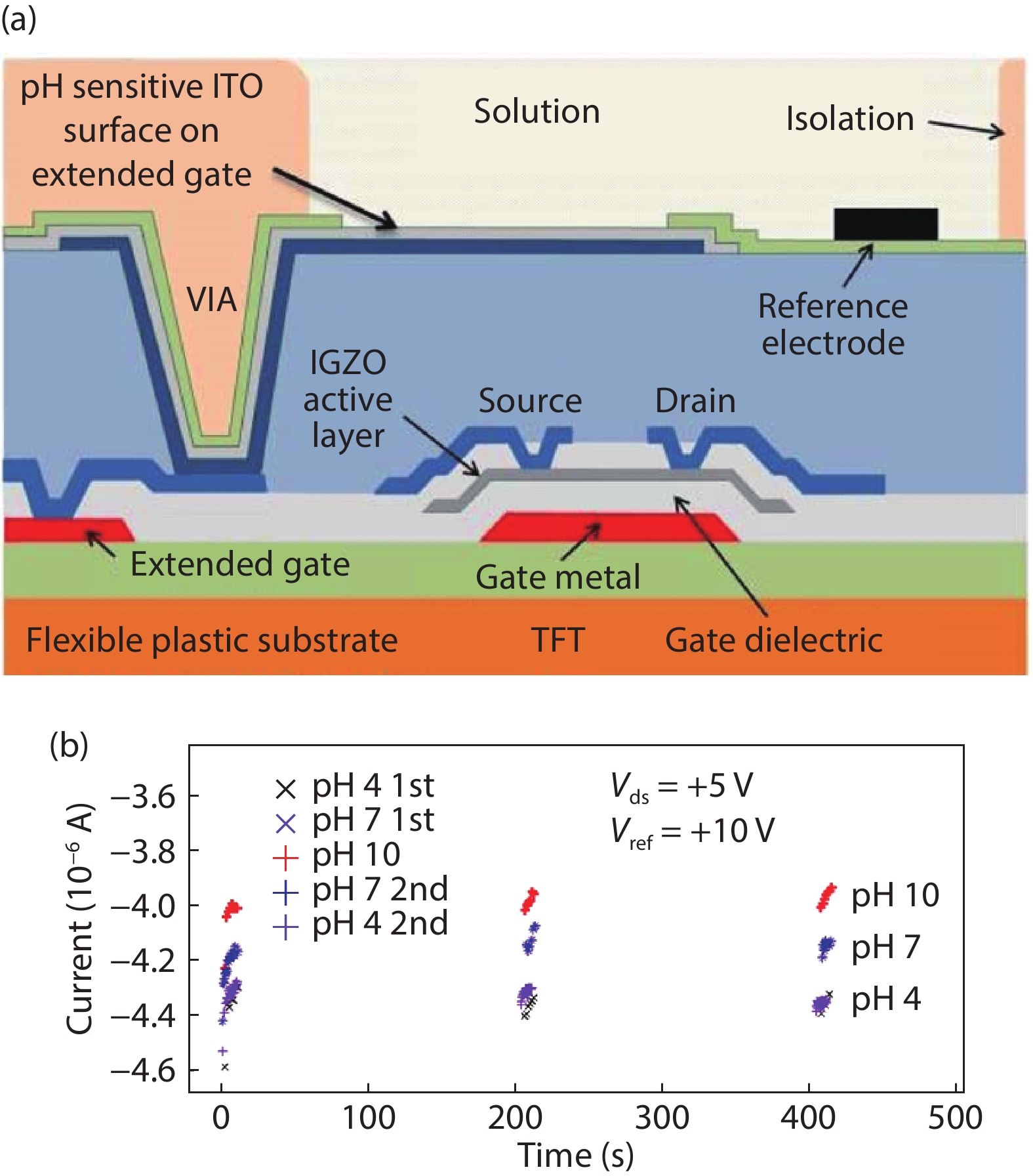
Fig. 16 (Color online) (a) Structure of the flexible extended-gate ISFET pH sensor. (b) Data graph of the drain current vs time[19].
Download figure:
Standard image3.2.4. Gas sensors
Gas sensors based on IGZO-based TFTs are used to detect both oxidizing and reducing gases (like NO2 and H2)[29, 137-139]. Oxidizing or reducing gas molecules act like electron acceptors or donors to change the carrier concentration, respectively, and thus change the drain current of the IGZO-based TFTs[30]. For example, Lee et al. reported a H2 sensor using the IGZO-based TFTs[138]. Palladium (Pd) was used as source/drain electrodes and also used to detect hydrogen (H2) gas concentration. The drain current increased as the Pd and IGZO interface barrier height decreased, which happened because of the formation of a hydrogen dipole layer at the interface[139]. To sense the reducing gas, Kim et al. presented a low-concentration NO2 gas detector. The a-IGZO thin film was used both as a channel and as a sensing layer[137]. Fig. 17 shows the device structure, transfer curves under 50 ppm NO2 gas concentration with different times, and the drain current change as a function of the exposure time, respectively. The threshold voltage positive shifted with an oxidation reaction in the NO2 gas, NO2 (gas) + e– (surface of oxide) → NO 2 (adsorbed). In particular, the sensing data was accurately obtained from the variation of the drain current and this sensor achieved efficient detection of the variation of the NO2 concentration. Thus, a-IGZO TFT-based gas sensors show good responsivity, sensitivity and recovery from the low concentration of the NO2 gas.
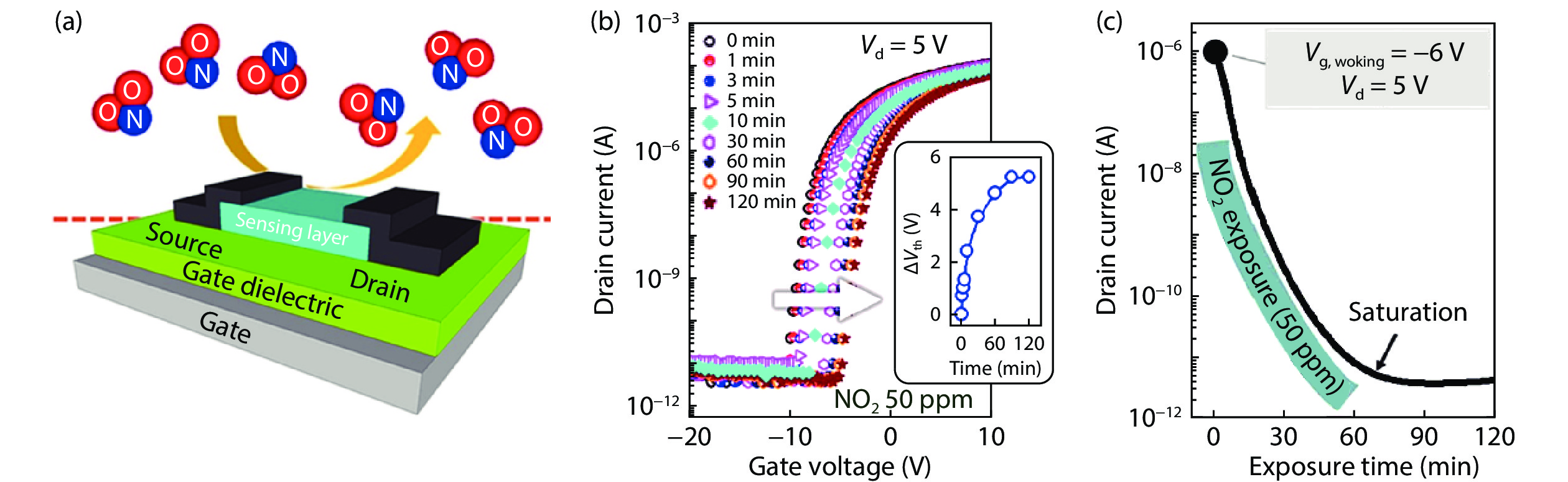
Fig. 17 (Color online) (a) Schematic diagram of the IGZO-based TFT structure. (b) Transfer curves with different time under 50 ppm NO2 gas concentration. (c) Drain current vs time under 50 ppm NO2 gas concentration[137].
Download figure:
Standard image3.2.5. Flexible sensors
IGZO-based TFT sensors have been widely used in flexible light detectors, pH sensors, gas detectors, and so on[19, 22, 33, 140]. For example, Xin et al. presented a novel pressure-sensing system using an a-IGZO-based TFT configuration comprised of a microstructured polydimethylsiloxane (PDMS) capacitor[22]. Fig. 18 shows the structures and the output curves, respectively. This array was fabricated on a highly flexible PI substrate using the back channel etch structure. The mechanism of the device can be explained by the change of the capacitance of the microstructured PDMS under an external pressure to modulate the gate voltage and change the output drain current. This device shows sufficient sensitivity to detect pressure difference under extremely low-pressure regime. The microstructure PDMS thin film showed good sensitivity of 0.1 kPa–1 and response time of lower than 190 ms for the pressure of 12 kPa. According to the amplification effect of the a-IGZO-based TFT, the device showed a high sensitivity in the subthreshold region for the ultra-low-pressure (≤ 1.5 kPa) detection and good linearity in the linear region for low-pressure (≤ 7 kPa) detection. The results demonstrated that a novel approach can be used for pressure-sensing intelligent products.
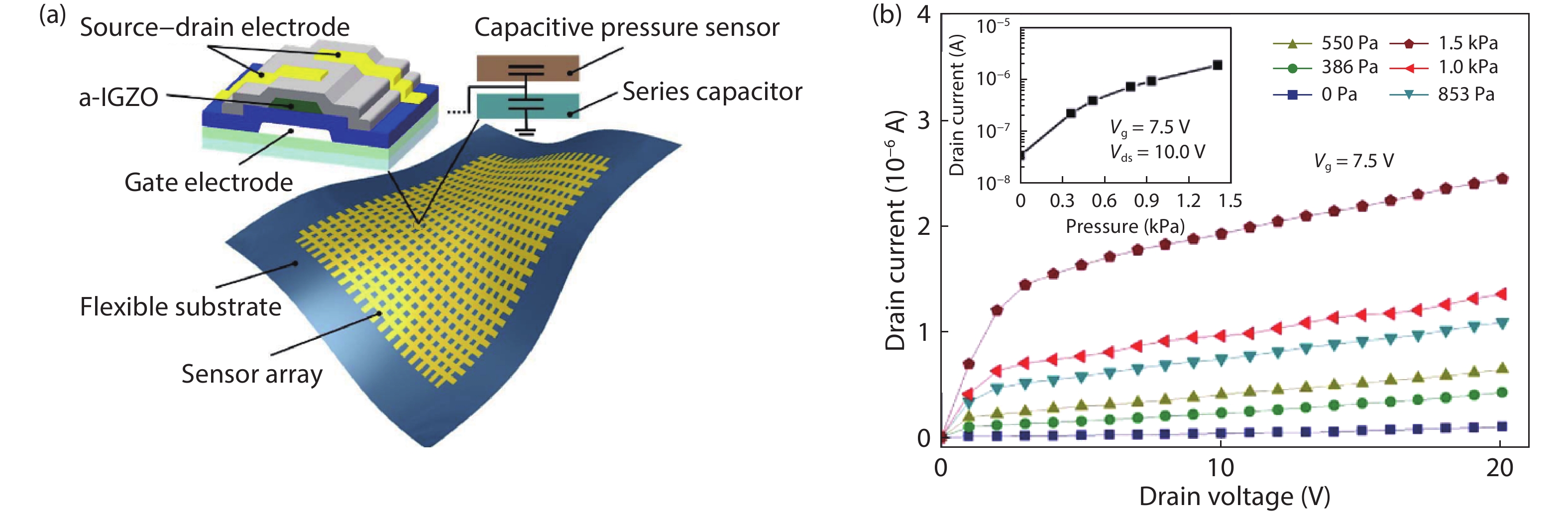
Fig. 18 (Color online) Schematic diagrams of the a-IGZO-based TFT pressure-sensing system and output curves[22].
Download figure:
Standard imageFlexible IGZO-based TFTs are especially capable for use as flexible circuits, such as oscillators, inverters, radio frequency identifications, operational amplifiers and clock generators[87, 141-143]. Thus, flexible sensors provided by flexible circuits have aroused a great deal of interest[47, 144]. For example, Meister et al. reported a low-power low-frequency light-sensing oscillator with IGZO-based TFTs that were integrated on a bendable plastic substrate[47]. This oscillator could be directly used as a light sensor without additional read out circuits. The device oscillated between 5 Hz in the dark and 31 Hz under daylight. The light-sensitivity of the oscillation frequency is between 7.4 Hz/klx in the dark and about 1.7 Hz/klx in the daylight. In particular, this device had a low frequency of 5–31 Hz and low power of 188μW. Significantly, this work achieved a low-power consumption, flexible integrated circuit that can be directly used to sense the light intensity through the frequency of the oscillation in a small chip area.
Table 2 shows the recent studies of the sensor applications based on the IGZO-based TFTs. This table shows the substrate, structure, electrical properties and the specific sensor applications of the IGZO-based TFTs.
Table 2. Sensor applications of the IGZO-based TFTs.
| Substrate | Structure of the TFT | μFE(cm2V–1s–1) | Ion/Ioff | Vth(V) | SS (V/dec) | Application | Ref. |
|---|---|---|---|---|---|---|---|
| SiO2/Si | Top gate | 18 | ~106 | 0.6 | 0.07 | Photoelectric sensor | [145] |
| Si | Bottom gate | 10.8 | — | 2.3 | 0.34 | Phototransistor | [131] |
| Glass | Bottom-gate | 3 | 1.08 × 10⁵ | 0.5 | 0.49 | Deep-ultraviolet phototransistor | [146] |
| SiO2/Si | Double gate | 6.51 | 5 × 10⁶ | 0.51 | 0.12 | PH sensor | [136] |
| Si | Double gate | 4 | 107 | 2.8 | 0.31 | PH sensor | [126] |
| SiO2/Si | Bottom gate | 7.58 | ~107 | — | 0.49 | Gas sensor | [147] |
| — | Double gate | 13.8 | 2.9 × 10⁶ | 0.72 | 0.19 | Hybrid gas sensor | [30] |
| Glass | Bottom gate | 12 | — | 1.39–1.92 | 0.24 | Temperature sensor | [16] |
| Metal foil | Bottom gate | 21 | ~107 | 7.36 | 1.12 | Flexible thermal and pressure sensor | [148] |
| Polyimide | Back channel etch | 20 | 107 | 1 | — | Flexible pressure sensor | [149] |
| Polyethylene naphthalate | Bottom-gate | — | — | — | — | Biosensor | [19] |
| Polyethylenenaphthalate | Bottom-gate staggered | 10~15 | — | 2 | 0.3 | Flexible X-Ray detector | [150] |
| Polyimide | Bottom-gate inverted staggered | 13.34 | — | 0.87 | — | Flexible gas sensor | [140] |
3.3. Neuromorphic systems
Traditional computers based on von Neumann architectures play essential roles in almost every field and have led to the development of information technology. However, there are two main problems that hinder the further improvement of computing power: the first is the limitation on energy efficiency as we approach the end of the Moore's law and the second is the challenge of the von Neumann bottleneck. According to Moore's law, device size was made smaller and smaller. However, at present, the device size is close to the physical limit and Moore's law is gradually failing. Meanwhile, information processing in the von Neumann computer requires the transmission between processor and memory units, which is unfavorable for computational efficiency and the size of the architecture. As computing speed increases, the energy consumption becomes larger. In the famous man-machine battle, the power of the artificial intelligence AlphaGo is about 150 kW. These problems of von Neumann computers will become more serious with the spread of the Internet of Things and artificial intelligence. As an efficient solution for complex data processing, neuromorphic electronics that emulate the functions and the information processing of the human brain have been proposed.
The human brain is a highly efficient computing system that can process input information and react to external stimuli with ultralow energy consumption of ~20 W and small volume occupation of ~1200 cm3 [151]. Neurons are often considered as the computational engines of the human brain. The signals conducted between neurons depend on the recent activities at either or both sides of the synapse. The connection strength between synapses is known as synaptic plasticity. Synaptic plasticity consists of three different styles: 1) long-term plasticity, in which the change of synapses can last for hours or longer and is considered to be memory; 2) homeostatic plasticity, which keeps the neurons in an appropriate state; and 3) short-term plasticity, in which the signals that occur in the synapses last for milliseconds or minutes, and is considered as a critical computational function in neural systems. Synapses are the basic units of computing and learning in the human brain. To build artificial neuromorphic systems inspired by the human brain, the basic requirement is to prepare a device that can simulate synaptic behaviors. In the past few years, complementary metal oxide semiconductor (CMOS) integrated circuits have been used to mimic the synaptic functions, such as IBM's TrueNorth chip that integrated 5.4 billion transistors to simulate 1 million neurons and 256 million synapses[152]. However, large-scale CMOS-based analog circuits consume a large amount of energy, which hinders the development of the CMOS synaptic applications. In recent years, the design of a single device that mimics synaptic functions has received a lot of attention, such as two-terminal memristors[153-156]. Two-terminal memristors consist of three layers, two electrodes for sending and receiving information, and a 'storage' layer between them to memorize the information. Although two-terminal memristors possess the advantages of small size, simple device structure and low-energy consumption, the instability of the device and the integration difficulty may hinder their application in neuromorphic systems. Recently, three-/multi-terminal transistors have attracted much attention[157]. Unlike two-terminal memristors, these transistors have a gate to control the channel conductance and the energy consumption of the device can be lower. Furthermore, three-/multi-terminal transistors have good stability, controllable parameters and easy integration. For the emulation of synaptic behaviors, as shown in Fig. 19, the gate electrode is used as the presynaptic terminal and the channel layer with source/drain electrodes is considered as the postsynaptic terminal. The information transmission and process in the synapse starts from the triggering of the presynaptic pulse. Then, electrical activities in the pre-synapse are converted to the release of neurotransmitters and the post-synapse receives the neurotransmitters. Consequently, the current/potential of the post-synapse is changed. When a pulse voltage is applied to the gate electrode, the conductance of the channel layer is changed, which can be measured by applying a small voltage between the source and drain electrodes.
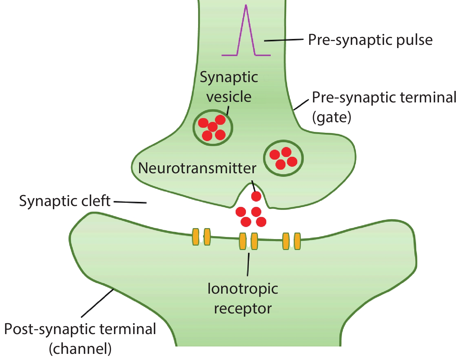
Fig. 19 (Color online) Schematic diagram of an artificial synapse based on neuromorphic transistor.
Download figure:
Standard imageHerein, we will demonstrate the works reported by our group about the application of IGZO-based TFT in synaptic networks and neuromorphic systems[35-37, 42, 43, 45, 158-161]. As early as 2009, Jiang and Wan et al. reported the first ultralow-voltage IGZO-based electric-double-layer (EDL) TFT[44]. This TFT exhibited an ultralow operation voltage about 1.0 V, a high μFE of 28.5 cm2/(V·s), and a low SS of 110 mV/decade. This ultralow-voltage operation was ascribed to the large EDL capacitance. Usually, in a liquid or solid electrolyte, mobile cations and anions are filled between two electrodes. When an external voltage is applied to the electrodes, the cations and anions will move to the surface of electrolyte/electrode, respectively, which is the charging process and will contribute a large EDL capacitance[162]. In our work, the proton H+ in mesoporous SiO2 moved from one bridging oxygen atom to another. When a negative dc voltage was applied to the gate electrode, the H+ would move to the dielectric/channel interface. Simultaneously, the electrons in the n-type IGZO channel accumulated near the interface, due to the combination of the gate potential bias. Importantly, this work laid a solid foundation for the follow-up research of IGZO-based TFT artificial synapse devices.
It is essential for synaptic transistors to have low-energy consumption. Zhou and Wan et al. presented flexible EDL IGZO-based TFTs with the energy consumption as low as 0.23 pJ/spike[161]. In this work, short-term synaptic plasticity and high-pass filtering behaviors are also mimicked. Figs. 20(a) and 20(b) show the structure of the device and a simple image of the artificial synapse, respectively. The artificial synapse is composed of an IGZO transistor. The gate is considered as the pre-synapse and the channel is considered as the post-synapse. When the voltage pulse is applied to the gate, a spike could be measured in the drain electrode, which simulates the information transfer process in the synapse. Fig. 20(c) shows the paired-pulse facilitation (PPF) curve that the excitatory postsynaptic current (EPSC) triggered by a pair of gate voltage spikes. The PPF reached a maximum value of 192% when the time interval was 20 ms, and it was reduced to 100% because the time interval is long enough. When the time interval between the pair of gate voltage spikes is shorter than the relaxation time of the protons in the nanogranular P-doped SiO2, some of the protons could not diffuse back to their equilibrium position before the second spike arrives, causing a large PPF. However, with the increase of the interval time, the protons gradually move back to their equilibrium position and the PPF gradually decreases. Fig. 20(d) shows the EPSC amplitude gain as a function of spike frequency. As the frequency of the voltage train changed from 1 to 50 Hz, the gain increased from ~1.0 to ~3.7. These results demonstrate the high-pass synaptic dynamic filtering of the IGZO-based neuromorphic TFTs.
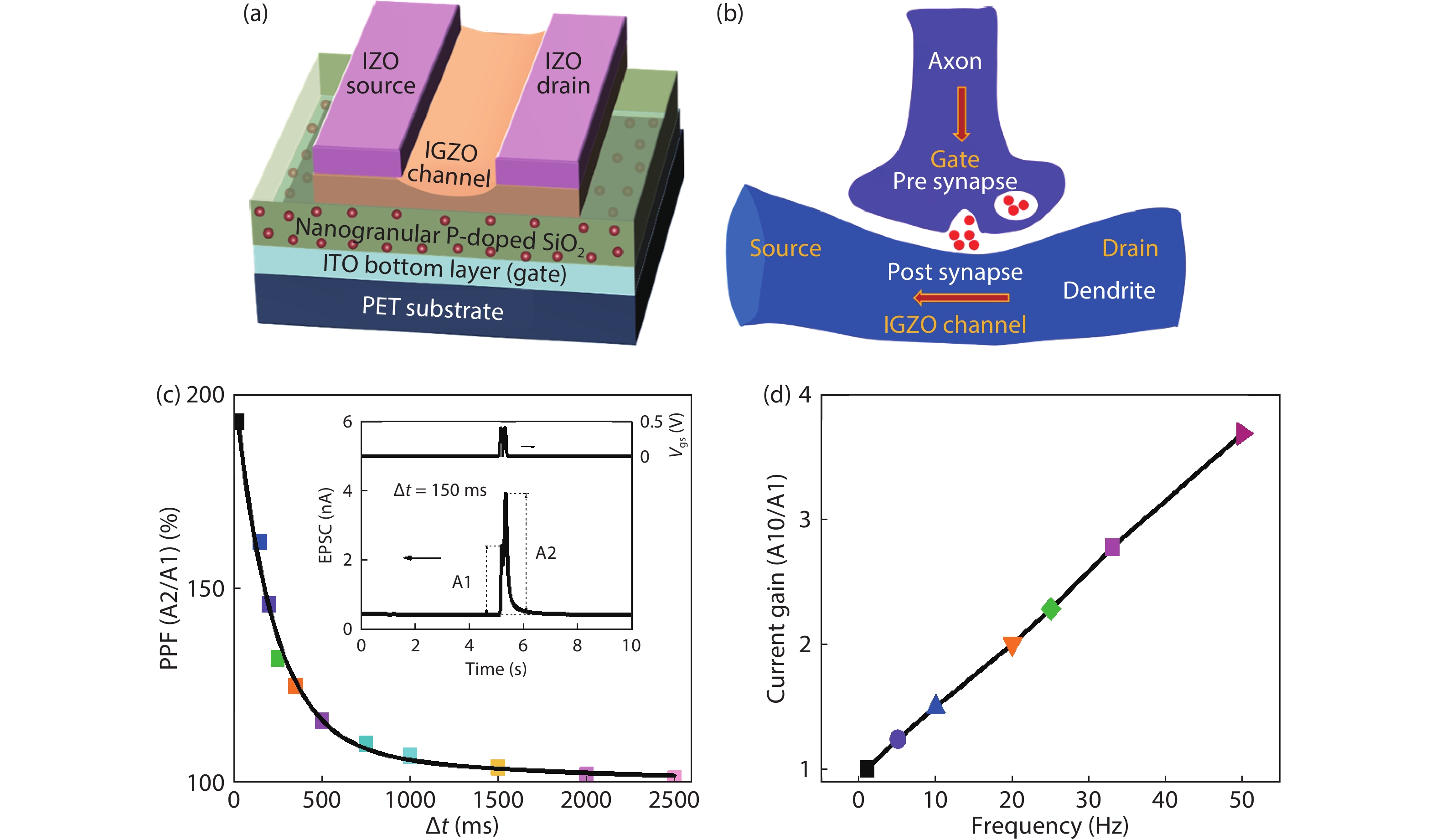
Fig. 20 (Color online) (a) Schematic diagram of the electric-double-layer (EDL) IGZO-based neuromorphic TFT structure. (b) Simple schematic diagram of an artificial synapse based on the IGZO-based TFT. (c) PPF ratio as a function of the time interval between the two stimuli spike. (d) EPSC amplitude gain as a function of spike frequency[161].
Download figure:
Standard imageEmulation of the short-term synaptic plasticity and synaptic filtering based on IGZO-based EDL TFTs was proposed by Wan et al.[45]. To simulate the synaptic facilitation and depression function, a three-terminal device was reduced to a two-terminal synaptic device. High-pass and low-pass filtering were successfully simulated. Figs. 21(a) and 21(b) show schematic images of the IGZO-based EDL TFT. In Fig. 21(a), the drain electrode and gate electrode were shortly connected as the presynaptic terminal. When we applied a positive voltage to the drain electrode, the protons in the electrolyte migrated to the IGZO channel/electrolyte interface. The EPSC was increased and the facilitation simulation was achieved. Fig. 21(b) shows that the source electrode and gate electrode were shortly connected as post-synapse terminal to emulate the short-term depression behavior. When the positive spike was applied to the drain electrode, the protons in the electrolyte migrated to gate electrode/electrolyte interface. The response current gradually reduced and synaptic depression can be obtained. Figs. 21(c) and 21(d) show the facilitation and depression simulations with the EPSC as a function of the pulse number and rate, respectively.

Fig. 21 (Color online) (a, b) Schematic images of the top-gate IGZO-based neuromorphic TFTs with electrolyte gate dielectric. (c, d) EPSC as a function of pulse number and rate of the positive presynaptic spike trains, respectively[45].
Download figure:
Standard imageOur brain contains more synapses than neurons, which guarantees multiple information processing. It is suggested that the multi-terminal neuro transistors are more suitable for complex neural network simulation[163]. He and Wan et al. proposed capacitively coupled multi-terminal IGZO-based neuromorphic TFT and neural network for spatiotemporal information processing[36]. The multi-gate terminals and the channel of the TFT are coupled by strong lateral ionic/electronic coupling effect. In the simulation, electric pulse sequences applied on the multi-gate are used as spatiotemporal information and the response is read from the source/drain. Multi-gate terminals and source/drain electrodes are used as presynaptic neuron (PREN) terminals and postsynaptic neuron (POSTN), respectively. A neural network consisting of two PRENs and POSTNs was proposed to emulate the sound azimuth detection as shown in Fig. 22(b). PREN1 and PREN2 are used as left and right ear sensing neurons, respectively. Fig. 22(a) shows a schematic diagram of sound location of the ears. An electrical pulse is applied on PREN2 and then the same pulse is applied on PREN1 when the sound is from the right direction, and vice versa. The time interval represents the sound azimuth. Fig. 22(c) shows that the POSTN1 and POSTN2 could produce different response (IPOST1 and IPOST2) to the sound direction. Fig. 22(d) shows that the ratio of the amplitude of IPOST2 and IPOST1 varies with the sound azimuth. Thus, the neural network can realize sound azimuth detection function. A network that can realize spatiotemporal information processing is of great interest for brain-like computing in the future.

Fig. 22 (Color online) (a) Schematic diagram of sound location of the human brain. (b) Schematic picture of the IGZO neuromorphic device and neural network for the emulation of sound azimuth detection. (c) IPOSTN1 and IPOSTN2 when the sound comes from the right direction. (d) The ratio of IPOST2 and IPOST1 as a function of the sound azimuth[36].
Download figure:
Standard image4. Conclusions and outlook
In this review, we have discussed IGZO materials, devices and recent developments of the IGZO-based TFT applications. In the introduction, the history, electron travelling orbitals and deposition methods of the IGZO materials are presented. Then, capitalizing on the unique properties of IGZO-based TFTs, such as relatively high mobility, good optical transparency and good compatibility with traditional CMOS technology, numerous devices based on IGZO-based TFTs have been demonstrated. For these applications, IGZO-based TFTs are not only promising candidates for display applications but are also actively involved in sensor applications and neuromorphic systems.
Great progress has been made in implementing IGZO-based TFTs into mainstream display technologies such as LCDs and OLEDs. However, the brightness uniformity of the panel, the stability of the device and the yield hinder the progress of the high ppi, the large size, the narrow bezel and the true flexible display panels. We believe that these problems will be overcome in the not-too-distant future and that the IGZO-based TFTs will gradually dominate the display market. The application of display derivers may be the main development direction of the IGZO-based TFTs in the future.
Based on the state-of-the-art understanding of the properties of the IGZO-based TFTs, multifunctional sensors such as photoelectric sensors, pressure sensors, pH sensors and gas sensors have been fabricated. Nevertheless, the low detection precision hinders their further application in the field of sensing. For pH sensors, the pH sensitivity based on the ISFET is limited by the Nernst limit of about 59 mV/pH. For photoelectric sensors, the persistent photoconductivity effect has greatly limited the detection accuracy. However, by optimizing thin-film fabrication strategies, the structure of the device and the fabrication technology, it is predicted that sensors based on IGZO-based TFTs will appear in consumer products.
Although some neuromorphic devices based on IGZO-based TFTs have been fabricated and some important synaptic/neuronal functions have been emulated, the development of the emerging neuromorphic device and system is still in its early stage. There is still a lot of room for optimization in device technology and structure. In the future, three-dimensional integration is one of the most important issues for a large-scale neuromorphic system. Finally, the key challenge for brain-like computing and perception is to explore and understand the spatiotemporal dynamic algorithm used in our brain. Consequently, interdisciplinarity between microelectronics and neuroscience is crucial for disruptive innovation in neuromorphic system.
Acknowledgements
The authors are grateful for the financial support from the National Natural Science Foundation of China (Grant No. 62074075, 61834001), and the National Key R&D Program of China (Grant No. 2019YFB2205400).