


Abstract
We present a review on recent work performed on periodic complex metallic alloy (CMA) surfaces. The electronic and crystallographic structures of clean pseudo-tenfold, pseudo-twofold, sixfold surfaces will be presented along with the recent findings on CMA of lower structural complexity, i.e. with a smaller unit cell. The use of CMA surfaces as templates for thin film growth and the formation of surface alloy will also be introduced. The reactivity of these complex surfaces and their impact in the field of heterogeneous catalysis will be discussed. Finally, common trends among these systems will be highlighted when possible and future challenges will be examined.
Export citation and abstract BibTeX RIS

Content from this work may be used under the terms of the Creative Commons Attribution-NonCommercial-ShareAlike 3.0 licence. Any further distribution of this work must maintain attribution to the author(s) and the title of the work, journal citation and DOI.
1. Introduction
The surfaces of bulk alloys have long been of interest for their potentially useful chemical properties, like improved activity and/or selectivity to certain reactions in catalysis or improved passiveness to corrosion for example. To understand these phenomena, it is necessary to study the structural, electronic and chemical properties of alloy surfaces at an atomic scale. Following the development of ultra-high vacuum (UHV) technology and associated surface science techniques, this field of research has been expanding since the 1970s. There is a vast literature on the subject, mainly focussing on binary compounds with unit cells typically containing less than ten atoms [1, 2]. In these simple compounds, complex phenomena already occur. The surface structure and chemical composition of alloys commonly differ from those expected from a simple bulk truncation, because of segregation and chemical ordering phenomena.
It was thus quite audacious to initiate the first surface studies of quasicrystals in the 1990s, soon after the synthesis of the first single grains of these new materials [3–5]. Indeed quasicrystals represent the ultimate complexity among intermetallics, being mainly ternary compounds, possessing no unit cell and no translation periodicity. Many exciting questions were raised concerning the nature of a 2D truncation of a 3D quasicrystal. In particular was the question regarding the influence of the cluster building blocks of quasicrystals on the surface morphology. Surprisingly, the results of surface investigations led to relatively simple answers. Quasicrystalline surfaces can be prepared by usual sputtering and annealing cycles in UHV conditions. It leads to a terrace and step morphology, similar to what is known for simple alloys. It is generally admitted that there is no surface chemical segregation, at least in Al-TM-TM (TM: transition metal) quasicrystals. The mechanism by which the surface free energy is minimized in such systems is by selecting only specific planes of the bulk structure as surface termination, thus satisfying simultaneously the ordering tendency of the alloy and having only (or mainly) the element with the lowest surface energy γ at the surface [6–9]. In the case of Al-based quasicrystals, the surface is found to terminate at dense A1-rich planes of the bulk. These planes are atomically flat and they intersect the 3D cluster packing. Therefore, there is no obvious influence of the cluster units on the surface morphology in this case. A similar conclusion has been reached for non-Al-based quasicrystal i-Ag-In-Yb for which the surface terminates at dense Yb-rich planes of the bulk structure intersecting the rhombic triacontahedral cluster units [10]. Thus, the quasiperiodic structure is preserved at quasicrystalline surfaces as well as the pseudogap in the electronic density of states (DOS) characteristic of the bulk. The origin of the pseudogap is usually ascribed to the Hume–Rothery effect combined with sp-d hybridization in Al-TM-TM quasicrystals [11]. However, the magnitude of the pseudogap is expected to be reduced due to the lower coordination of surface atoms. This has been predicted based on density functional calculations performed for model approximant systems [12]. Apart from atomic and electronic structure investigations, most of the properties of quasicrystalline surfaces under UHV conditions relate to adsorption of metals and molecules, chemical reactivity as well as adhesion and friction [13–15]. Adsorption experiments have shown that truncated clusters are frequently preferred adsorption sites for adsorbates and this peculiarity has allowed for the growth of artificial 2D pseudomorphic thin films. Chemical reactivity studies are still relatively scarce except for oxidation studies of Al-based quasicrystals motivated by initial report of excellent oxidation and corrosion resistance [15–17]. However, the first experiment of oxygen adsorption on quasicrystal surfaces quickly demonstrated that the oxidation characteristics are similar to those of aluminium with the existence of a chemisorbed phase which destroys the quasiperiodicity of the surface. This chemisorbed phase is a precursor to the formation of a thin (4–8 Å) aluminum-rich amorphous oxide layer. The oxidation kinetics is nevertheless different because of the low diffusivity of the elements in the quasicrystal once the passivation layer has been formed. This leads to thinner oxide thin films even under high temperature oxidation conditions. Also the nature of the amorphous oxide appears to be different on the quasicrystalline substrate, being more ionic compared to the native oxide formed on aluminum under dry conditions [18]. Adhesion and friction have been investigated on clean quasicrystalline surfaces by atomic force microscopy [19, 20]. Two interesting properties were highlighted by these experiments: low adhesion and friction anisotropy. The low adhesion forces measured compared to normal metals is related to the electronic structure of the quasicrystalline surface. We refer interested reader to specific reviews for more detailed information on the surface structure and properties of quasicrystalline surfaces [9, 14, 21–25].
In this review, we will focus on another class of alloys of intermediate complexity that bridge the gap between simple alloys mentioned earlier and quasicrystals. They are complex metallic alloys (CMA) characterized by large unit cells containing several tens of atoms, usually arranged into geometrical clusters related to those found in quasicrystals. Some of the compounds are real approximants of quasicrystalline phases in the sense of the cut and projection method while others only share some similarities with quasicrystals but are not approximant phases. A list of the various systems investigated so far is provided at the end of this review, together with the appropriate references. Surface studies of these CMA compounds allow for a better understanding of the interplay that exists between bulk and surface structures. It will be shown for instance that the bonding network characterizing most of these intermetallic compounds influences often considerably the resulting CMA surface structures, effects that can only be fully understood using ab initio calculations. Therefore, periodic CMAs of moderate unit cell size compatible with today's computational limits, constitute a new playground for investigation of alloy surfaces.
2. Approximant surfaces
2.1. The pseudo-tenfold surface of the  -Al-Pd-Mn crystal

To our knowledge, the first experimental surface study of an approximant was performed on the  -Al-Pd-Mn crystal [26]. This phase is orthorhombic with the space group Pnma and lattice parameters a
 = 23.4 Å, b
 = 16.5 Å and c
 = 12.4 Å (320 atoms per unit cell). It is an approximant of the icosahedral i-Al-Pd-Mn quasicrystals and contains pseudo-Mackay clusters similar to those found in the quasicrystalline structure. The structure along the [010] direction—which is the pseudo-tenfold direction—can be described by a stacking of flat and puckered layers as shown in figure 1. Single crystals of this phase could be obtained either by Bridgman (BG) or by self-flux (FG) methods with composition
  -
- and
and  -Al
-Al Pd
Pd Mn
Mn respectively. However, the FG sample contained defects and we will thus only describe the results obtained on the BG sample. The pseudo-tenfold (p-10f) surface of this sample has been investigated using scanning tunnelling microscopy (STM), low-energy electron diffraction (LEED) techniques and reflection high energy electron diffraction (RHEED) [26, 27]. After sputtering the
  -Al
-Al Pd
Pd Mn
Mn surface, the RHEED patterns are consistent with the formation of one domain of a simple cubic lattice with (100) surface plane. From the diffraction and chemical analysis, this surface structure is related to the CsCl-type Al-Pd phase [27]. The presence of a single domain as opposed to multiple twinned domains is explained by the relatively small lattice mismatch between the Al-Pd alloy and the bulk, i.e. a small strain at the interface. Upon annealing, the LEED pattern exhibits the expected p-10f symmetry. The step heights determined by STM are equal to half the period along the
  axis (b/2). The consequence of this unique step is that surface termination corresponds to particular pair of layers related to each other by a mirror plane
1
. A striking feature revealed by STM is that the surface plane is incomplete as seen in figure 1. It consists of bright dots randomly occupying the centre and the nodes of the substrate unit cell. The dots are attributed to Al decagonal rings identified as part of the pseudo-Mackay clusters decorating the rectangular unit cell at y = 0.25. They must be formed during the surface reconstruction upon annealing and are found to be relatively stable. They form an incomplete surface layer that lies on top of a dense termination consisting in the second and third layers. These two layers are separated by only 0.066 nm and can thus be considered as a single termination, the density of which is larger than that of first and fourth layers. Altogether, the second and third planes covered by Al decagonal rings form a dense Al-rich termination. Therefore, one can say that the principles guiding the surface plane selection are the same for the
axis (b/2). The consequence of this unique step is that surface termination corresponds to particular pair of layers related to each other by a mirror plane
1
. A striking feature revealed by STM is that the surface plane is incomplete as seen in figure 1. It consists of bright dots randomly occupying the centre and the nodes of the substrate unit cell. The dots are attributed to Al decagonal rings identified as part of the pseudo-Mackay clusters decorating the rectangular unit cell at y = 0.25. They must be formed during the surface reconstruction upon annealing and are found to be relatively stable. They form an incomplete surface layer that lies on top of a dense termination consisting in the second and third layers. These two layers are separated by only 0.066 nm and can thus be considered as a single termination, the density of which is larger than that of first and fourth layers. Altogether, the second and third planes covered by Al decagonal rings form a dense Al-rich termination. Therefore, one can say that the principles guiding the surface plane selection are the same for the  phase and its i-Al-Pd-Mn quasicrystalline counterpart. However, the existence of these Al decagonal rings indicate preferential re-growth during the annealing step at sites that are part of the pseudo-Mackay cluster units in the case of the
  approximant. This is not the case for the quasicrystal, where re-growth encompasses not only cluster sites but also glue sites connecting the cluster units. This raises the question of the relative stability of the cluster units, which may not depend solely on the cluster themselves but also on the way they are connected, i.e. on glue atoms.
Figure 1. (a) Structure model of the  -Al
-Al Pd
Pd Mn
Mn orthorhombic phase according to Boudard et al [28]. Flat (F) and puckered (P) layers are stacked along the pseudo-tenfold direction (b axis). (b) STM image (100 × 100 nm
 ) of the pseudo-tenfold surface of the
  -Al
-Al Pd
Pd Mn
Mn [26]. The terraces are covered by dots of bright contrast which are identified as decagonal rings of Al atoms decorating the unit cell as shown in the image (10 × 10 nm
 ) in (c). The yellow (white) rectangles give the surface unit cell dimensions [26].
Download figure:
Standard image High-resolution image2.2. The (010) surface of the T-Al(Mn, Pd) crystal

Similarities can be outlined between the p-10f surfaces of  -Al-Pd-Mn and T-Al
 (Mn, Pd) approximants
2
. The latter surface has been recently investigated using experimental and computational techniques [30]. LEED and x-ray photoelectron diffraction (XPD) patterns confirm the p-10f symmetry of the sample. Height profile measurements across several terraces exhibit a main step height, which corresponds to half of the lattice parameter along the [010] direction. High-resolution STM images indicate structural imperfections on individual surface termination. Using a tiling approach (see figure 2), the local atomic arrangement observed on terraces is only compatible with one of the two types of puckered layers present in the bulk model. This latter plane, referred to as P
(Mn, Pd) approximants
2
. The latter surface has been recently investigated using experimental and computational techniques [30]. LEED and x-ray photoelectron diffraction (XPD) patterns confirm the p-10f symmetry of the sample. Height profile measurements across several terraces exhibit a main step height, which corresponds to half of the lattice parameter along the [010] direction. High-resolution STM images indicate structural imperfections on individual surface termination. Using a tiling approach (see figure 2), the local atomic arrangement observed on terraces is only compatible with one of the two types of puckered layers present in the bulk model. This latter plane, referred to as P in [31], is composed of both Al and transition-metal (TM) elements with mixed occupancy, hence explaining both the heterogeneous decoration on terraces and the bias dependence of the STM images. Within the Tersoff–Hamann approximation [32], the tunnelling current is assumed to be proportional to the integrated local electronic DOS in the range [E
 ; E
; E ±V
±V ]. The electronic DOS of TM elements exhibits usually a higher degree of asymmetry relative to the Fermi level than the sp metal-like Al band. For systems where the TM d-like band dominates the DOS at E
 , one should expect a drastic variation of the STM image contrast when using opposite bias (probing (un)filled states). Although other parameters can alter the STM image contrast (for more information see [33]), the bias dependence reported here originates from the contribution of Mn d-band at E
 . Using ab initio calculations, it has been possible to determine the cleavage plane. An expansion of the lattice parameter b by 50% followed by a structural relaxation leads to a cut between consecutive P
 -type planes within the bulk model, hence leaving P
 layer as the most favourable surface termination. The associated simulated STM images are qualitatively in good agreement with the experimental images and replicate the observed bias dependence. The electronic structure of the T-Al
 (Mn, Pd) analysed by photoemission spectroscopy and ab initio calculations exhibits a shallower pseudogap compared to the i-Al-Pd-Mn quasicrystal due to an enhanced Mn d contribution to the DOS at the Fermi level [30].

Figure 2. (a), (b) 4 nm × 4 nm high resolution STM images recorded on two different regions on the same surface. (c), (d) A tiling used to describe the puckered layer (P ) has been superimposed on both STM images. While positioned identically with respect to the tiling, the contrast within the largest pentagons varies drastically within the same image and between both images of opposite bias [30]. Reprinted with permission from [30]. Copyright (2010) by the American Physical Society.
Download figure:
Standard image High-resolution image2.3. The (001) surface of the μ-AlMn crystal

In order to investigate other CMA phases related to the quasicrystalline Al-Mn system, the sixfold (001) surface of the μ-Al Mn approximant has been selected and characterized using LEED and XPD techniques [35]. The sample
  has been grown from an Al-rich melt using the Czochralski technique. The crystal belongs to the P6
 /mmc space group with an unit cell containing 563 atoms and bulk lattice constants a = 1.998 nm and b = 2.467 nm. Only two Al positions exhibit partial occupancy. The bulk structure along the [001] direction can be described as a stacking of 12 layers. The flat layers are located at z = 0, 1/4, 1/2 and 3/4 (labelled 0c, c/4, c/2 and 3c/4 in [35]). The remaining eight puckered layers are distributed by pairs between the flat layers (see figure 3(a)).
Figure 3. (a) Representation of the μ-Al Mn structure along the [001] direction from [34]. LEED patterns obtained on the μ-Al
 Mn(001) surface at (b) 21 eV and (c) 57 eV [35]. (Figures 3(b), (c) from [35], reprinted by permission of Taylor
  Francis Ltd, www.tandfonline.com.)
Download figure:
Standard image High-resolution imageAfter sputtering and annealing the sample to 920 K, a clean and terrace-terminated sixfold μ-Al Mn(001) surface is obtained and exhibits sharp diffraction LEED patterns (figures 3(b), (c)). In addition to the expected sixfold rotational symmetry, the LEED patterns are dominated by a series of diffraction spots of higher order with particularly strong reflections of the 1st, 3rd, 5th and 8th order. This sequence is reminiscent of consecutive numbers of the Fibonacci series. These strong intensities are associated in real space to hexagons related by a τ-inflation. A careful comparison between XPD images and single scattering cluster (SSC) calculations not only further supports a simple bulk truncated surface termination but also validates the structural model proposed by Shoemaker [36]. The XPD and SSC analysis indicate a preferential surface termination at z = c/4 and 3c/4 over z = 0c and c/2 [35].
2.4. The (100) and (010) surfaces of the Al(Cr,Fe) crystal

In parallel to the previous studies, experimental works have been performed on the (100) and (010) surfaces of the Al (Cr,Fe) crystal [37]. This orthorhombic decagonal approximant has the following unit cell parameters: a = 1.250 nm, b = 1.262 nm and c = 3.065 nm [38]. The single crystals have been grown using the Czochralski method from Al-rich off stoichiometric melts. For the Al
 (Cr,Fe)(100) surface, the LEED pattern exhibits both the pseudo-sixfold symmetry along with the underlying larger scale twofold symmetry of the surface. High quality STM images have been obtained and reveal a cluster-based structure across terraces (figure 4). The feature dimensions and orientations correspond to what is expected from the model. From the layer stacking along the [100] direction and the measured step height across terraces, two terminations coexist at the surface, each related to the other by inversion symmetry.
Figure 4. (a) STM image (300 Å × 300 Å) revealing terraces on the Al (Cr,Fe)(100) surface. The step height is measured at 5.8 ± 0.2 Å. (b) Structural model demonstrating the inversion symmetry of adjacent terraces [37]. (Figure reproduced from [37] with permission from Oldenbourg Wissenschaftsverlag, München).
Download figure:
Standard image High-resolution imageRegarding the Al (Cr,Fe)(010) surface, there is evidence for microfacetting in the LEED pattern recorded after annealing the sample to 873 K, indicating that the (010) plane is not the most stable surface. High quality diffraction patterns have been obtained for lower annealing temperatures. The LEED patterns exhibit the surface unit mesh along with the expected pseudo-tenfold symmetry. However, none of the preparations used has led to a terrace-step surface morphology suitable for STM analysis [37].
2.5. The (100) surface of the Y-AlNiCo crystal


As for the μ-Al Mn approximant, more than one surface termination has been reported for the Y-Al
 Ni
Ni Co
Co (100) surface. Indeed, three different surface terminations denoted A, B and C have been identified on this approximant, structurally and chemically related to the d-Al-Ni-Co(10000) quasicrystal surface [39]. All three surface terminations have been related to the densest bulk planes. Interestingly, this approximant surface exhibits three types of surface reconstructions, a phenomenon not observed until then on approximant surfaces. The nature of these surface reconstructions identified in the LEED patterns have been identified locally using STM. While termination C is not reconstructed, (2 × 1) reconstruction is observed on terraces A and both c(2 × 2) and (3 × 2) reconstructions are identified on termination B. It has been shown that the two partially occupied Al sites are strongly involved in the surface reconstruction, with occupancies that differ from the one expected on bulk planes. The doubling of the periodicity along the b axis is a common feature observed on all three surface reconstructions. This tendency towards reordering at the surface is also present on the two crystallographically inequivalent twofold planes (i.e. the (12110) and (10000) surfaces) of the d-Al-Ni-Co quasicrystal; facetting of the (12110) surface has been reported and the surface periodicity along [10000] direction varies depending on the composition of the decagonal phase considered [20, 40–42]. The periodicity reported (0.4 nm [20] and 0.8 nm [42]) also diverges between experiments carried out on quasicrystal surfaces of almost similar composition and for comparable surface preparation. It is likely that a small change in the sample composition would have a drastic effect on the final surface structure as discussed in the following section 2.6.
Low temperature scanning tunnelling spectroscopy (STS) measurements have been carried out on the d-Al-Ni-Co(12110) and Y-Al-Ni-Co(100) surfaces (see figure 5) [43]. As for the Al-Pd-Mn systems, the STS spectra are dominated by a large parabolic pseudogap centred at the Fermi level, reduction of the DOS attributed to the Hume–Rothery stabilization mechanism and/or to orbital hybridization. Single point spectroscopy measurements have revealed a locally varying fine structure, which appears as energy-dependent modulations superimposed on the large pseudogap. These spectral features confined in energy to about 50–150 meV have a spatial extent of 0.5 nm. In addition, this study demonstrates that the spatial variation of the fine structure correlates with the topographic structures on both surfaces. Moreover, specific electronic states are localized on equivalent topographic features regardless of the presence of the periodic or quasiperiodic long-range order [43]. With a spiky DOS and a spatial localization of electronic states, these results support the concept of virtual bound states as proposed in [11] 3 .
Figure 5. (a)–(e) STM images showing respectively the twofold d-Al-Ni-Co(12110) surface at 5.4 K and the Y-Al-Ni-Co(100) surface (A-type termination) at 5.7 K. (b), (c), (f) Spatially resolved maps of the background-subtracted differential conductance recorded along the quasiperiodic direction and the c-axis with different set points. (d), (g) These two graphs exhibit the averaged differential conductance spectra recorded on and between columns and the total averaged spectrum [43]. (Figure reproduced from [43], © IOP Publishing  Deutsche Physikalische Gesellschaft. CC BY-NC-SA.)
Download figure:
Standard image High-resolution image2.6. The pseudo-tenfold surface of the AlCo crystal


This section deals with the recent progress made on the structural analysis of the (100) surface of the Al Co
Co crystal. This approximant to the decagonal Al-Ni-Co quasicrystal belongs to the space group Pmn2
 with 102 atoms per unit cell. The structure of the bulk model can be described as a stacking of flat (F) and puckered (P) layers (each exhibiting a p-10f symmetry) along the [100] direction in a F
 P
P F
F
 sequence. Recent progress in crystal preparation using the Czochralski technique has led to the growth of large metallic alloy single crystals of Al
 Co
Co and Al
 Fe
Fe from Al-rich solutions [44]. With centimetre-size samples available, the physical properties of the Al
 TM
TM (TM = Co, Fe) systems have been characterized. It has been demonstrated that both magnetic and transport properties are anisotropic [45].
However, the first experimental and theoretical study of the Al Co
Co (100) surface has been performed on a sample grown by the BG technique [46]. In this study, a multi-technique approach combining experimental and theoretical methods has been employed. After annealing the sample to 1073 K, the XPD images measured for Al 2s and Co 2p reveal typical features of decagonal symmetry elements and resemble those collected on the d-Al-Ni-Co quasicrystal surface. The calculated XPD images based on SSC simulations using (in)complete bulk layers reproduce the experimental results (see figures 6(a)–(d)). Depending on the annealing temperature chosen to prepare the sample, two surface terminations (with drastically different atomic density) have been identified across terraces. For the high annealing temperature regime used, one termination preferentially desorbs, leaving the densest termination as the dominant surface plane [46]. The analysis based on STM measurements and ab initio calculations suggest that the topmost surface layer can be related to puckered planes present in the bulk model. However, these puckered layers are incomplete when exposed at the surface (similar to the observations reported in section 2.1), leading to a highly corrugated termination. Thus, the proposed surface unit cell is composed of 10 Al and 2 Co atoms as opposed to 22 Al and 4 Co atoms for a complete puckered bulk layer [46].

Figure 6. (a), (b) Experimental XPD images recorded for both emitters (Al 2s and Co 2p
 ) measured on the p-10f surface of the Al
 Co
Co crystal with an Al Kα x-ray source. (c), (d) Single scattering cluster simulations performed for both emitters using a cluster of 3016 atoms derived from the bulk model [46]. (e) Surface layer resulting from the simulated cleavage experiment. Dashed lines indicate two PB clusters. The strong and partially covalent vertical Co–Al–Co bonds between the tips of the PB clusters are indicated by red (the darkest) stripes. The P plane splits into two complementary parts, which are separated by a vacuum layer. The highly corrugated surface layer is refereed to as the Z termination in [49]. (Reprinted figures with permission from [46] and [49]. Copyright (2009, 2011) by the American Physical Society.)
Download figure:
Standard image High-resolution imageThe second structural analysis of the Al Co
Co (100) surface has been carried out on a sample grown this time by the Czochralski technique. This study combining dynamical LEED analysis, STM measurements and density functional theory (DFT) calculations has shown that the structure of the Al
 Co
Co (100) surface is consistent with a dense Al-rich plane with surface Co atom depletion [47]. Calculations of the relative surface energies of several models as a function of the chemical potential of Al have been carried out to identify the most stable structures. Simulated and experimental STM images have been compared to discriminate among the different possibilities of surface models. The LEED R factor has been calculated for 13 different models. The best-fit that emerges through these analysis is for a surface layer corresponding to a bulk puckered layer where all Co atoms have been removed
4
. Due to the step height measured at the
(100) surface is consistent with a dense Al-rich plane with surface Co atom depletion [47]. Calculations of the relative surface energies of several models as a function of the chemical potential of Al have been carried out to identify the most stable structures. Simulated and experimental STM images have been compared to discriminate among the different possibilities of surface models. The LEED R factor has been calculated for 13 different models. The best-fit that emerges through these analysis is for a surface layer corresponding to a bulk puckered layer where all Co atoms have been removed
4
. Due to the step height measured at the  (100) surface, both puckered layers (P
 and P
and P ) present in the unit cell are exposed at the surface, resulting in
  and
and  Al-rich terminations. The structure of these pure Al planes can be described by both sets of bipentagonal motifs interconnected via glue atoms. Depending on the method used to grow the crystals, significant differences in the glue atom density and surface roughness have been observed using STM [47]. The average relaxations of the surface layer P
 termination are +1% and −1% for the first two layers, while the situation is reversed for the P
 termination. This effect could be related to the opposite puckering direction of P
 and P
and P in the bulk structure [47].
These above-mentioned investigations have resulted in two structural models for the Al Co
Co (100) surface. While the two different growth techniques should lead to similar materials, it is possible that a minor change in the bulk composition has been introduced between the two specimens. This compositional variation will have to be very small if one considers the stability range of the Al
 Co
Co phase. In ordered alloys, there exists a discontinuity in the chemical potential at the stoichiometric composition. Hence, a slight compositional deviation from the ideal alloy stoichiometry should have a drastic effect on the chemical potential of Al in this particular case. These off-stoichiometric effects would eventually modify the surface energetics and consequently the resulting surface structure [48].
The same system has been simultaneously studied by Krajčí and Hafner using also ab initio density functional methods. As will be discussed below, different conclusions have been drawn for the Al Co
Co (100) surface structure [49]. Similarly to the approach for the T-Al
 (Mn, Pd) [46], the surface plane has been determined by a simulated cleavage experiment. Contrary to what was expected from experimental observations, the (100) surface is not formed by cleaving the crystal between adjacent P and F layers. In fact, the cleavage results in a split of the P layer into two complementary parts. The obtained structure preserves the integrity of the pentagonal bipyramid (PB) clusters identified as stable entities by a chemical bonding approach [50]. As shown in figure 6(e), the resulting surface structure (labelled Z termination) consists of an incomplete P layer, where only one set of bipentagonal motifs is preserved (the tip of PB clusters), and a partially exposed F layer in the interstices.
Thus, the surface structure deduced from the numerical cleavage [49] is different from the one presented using surface energy calculations in [47, 48]. Indeed, the numerical cleavage is done with the following constaint—the number of atoms in the simulation supercell should be constant, while the approach used in [47, 48] allows us to consider a large number of possible structural models for the surface, with different chemical compositions. Then, it appears that the two ab initio approaches result in the same structural model for a Co-rich alloy, while the dense Al-rich surface termination is calculated to be the most stable among all considered surface models for an Al-rich alloy, i.e. the resulting surface structure depends on the chemical potential of Al [47, 48].
These ab initio studies [47, 49] demonstrate that the surface structure may also differ depending on the surface preparation (cleavage at 0 K or sputter-anneal cycles to high temperatures). As presented in a previous study [51], the total DOS of the Al Co
Co crystal close to the Fermi level exhibits a narrow Co d band and a shallow pseudogap. At the surface, the depth of the pseudogap and the Co d band position will vary depending on the surface termination considered (for instance P or Z terminations) [49].
2.7. The pseudo-tenfold surface of the AlFe crystal


As for the Al Co
Co phase, anisotropic transport properties have been measured for the Al
 Fe
Fe crystal [52]. Regarding the surface properties, the Al
 Fe
Fe crystal has been recently proposed as a low-cost alternative material for heterogeneous catalysis [53]. Its catalytic performance is said to rely on small and well-separated atomic ensembles containing an active transition metal element at the crystal surface, also referred to as the site-isolation concept [54]. The stability of such ensembles under reaction conditions depends on the chemical bonding and on the intermetallic crystalline structure. Using a chemical bonding approach, the identification of several specific interactions have led to the description of the Al
 Fe
Fe as a cage compound where almost linear Fe-Al-Fe groups are encapsulated in cavities formed by a structurally complex Al network (see figure 7(b)) [50]. Quantum chemical calculations performed on the Al
 Co
Co system have highlighted similar covalent-like bondings within the orthorhombic unit cell. To understand the relationship that may exist between such interactions and the catalytic (surface) properties of the crystal, the Al
 Fe
Fe (010) surface has been analysed using STM, LEED and ab initio methods.
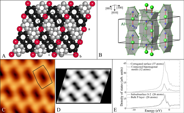
Figure 7. (a) Representation of the puckered (P) layer present in the Al Fe
Fe bulk structure. The black and gray atoms correspond to Al atoms forming pentagonal motifs. The red atoms are denoted 'glue' Al atoms. The empty and hatched circles are associated with Fe atoms located below and above the mean P plane position respectively. The irregular hexagon is obtained by connecting protruding Fe atoms. (b) Three-dimensional representation of the crystal structure where Fe–Al–Fe groups (host) encapsulated within Al cavities (cages) have been displayed. (c) 5 nm × 5 nm high resolution STM image (V
 = −1.05 V) after annealing the Al
 Fe
Fe (010) surface to 873 K. (d) Simulated STM image (V
 = −1 V) for an incomplete P layer that preserves the pentagonal bipyramid clusters at the crystal surface. (e) Electronic density of states calculated for the surface and subsurface layers of the Al
 Fe
Fe [55]. (Reprinted figure with permission from [55]. Copyright (2013) by the American Physical Society.)
Download figure:
Standard image High-resolution imageThe Al Fe
Fe crystal structure belongs to the C2/m space group. Its bulk structure can be described as a stacking of flat (F) and puckered (F) layers along the [010] direction. The layer sequence (F
 P
P F
F P
P ), the pseudo-tenfold symmetry and the 23-atom pentagonal bipyramid (PB) clusters used to described geometrically the bulk structure are common to both Al
 Co
Co and Al
 Fe
Fe crystals. As shown in figure 7(a), the puckered layer consists of bipentagonal motifs and Al glue atoms. Each Al pentagon is centred either by a protruding or a buried Fe atom. The connection of Fe atoms of one type (here protruding) results in an irregular hexagon. As for previous CMA systems, the surface preparation of the Al
 Fe
Fe crystal consists of cycles of sputtering and annealing to different temperatures. For a sample annealed to 873 K, angle-resolved x-ray photoelectron spectroscopy (XPS) measurements allow us to disregard any surface segregation and the LEED analysis (1 × 1 pattern) indicates that there is no surface reconstruction. At the surface, atomically flat terraces are separated by an unique step height (equal to b/2) which suggests either F or P layers as topmost terminations. Figure 7(c) shows a high resolution STM image where an irregular hexagon has been formed by connecting areas of bright contrast. The orientations and dimensions of this pattern are identical to the one drawn in figure 7(a). The motifs observed in this STM image can be described as pairs of adjacent protrusions aligned along the [101] direction (see for instance gray or black pentagons on figure 7(a)). They are reminiscent to the features reported on the Al
 Co
Co 100) surface, then associated with bipentagonal motifs present on the P layers [46, 47, 49]. To transform a P
 to a P
 layer, one has to mutually exchange one set of bipentagonal motifs by the other set, i.e. the gray (black) pentagons switch to black (gray) with protruding (buried) Fe atoms. As expected, this manifests itself on STM images by an apparent shift of the motifs/lines (propagating in the [101] direction) across consecutive terraces. From STM observations and previous studies carried out on structurally related systems, the surface terminations can only be related to P layers. From plot profile analysis at different STM bias, it appears that the dark contrast are related to deep trough. The position of these depressions indicates that the gray bipentagons are missing at the Al
 Fe
Fe (010) surface, i.e. the topmost surface layer corresponds to an incomplete P layer. With increasing annealing temperature, the surface structure evolves and partial desorption of Al 'glue' atoms occurs [55].
To complement the experimental evidence, ab initio calculations have been performed on this system. Following the above observations, a series of models derived from bulk truncation at P layer has been generated. A qualitative good agreement is obtained between simulated and experimental STM images (for a comparison see figures 7(c)–(d)) for a model where one set of bipentagonal motifs centred with buried Fe atoms (gray pentagons on figure 7(a)) have been removed from a P layer. In additional calculations, partial removal of 'glue' Al atoms replicates in fine detail the experimental images recorded on the Al Fe
Fe (010) surface annealed above 873 K. The total energy calculations indicate that the stability of the puckered layer is reduced incrementally with the removal of Al 'glue' atoms, i.e. as the density of the topmost termination is decreased. The layer-resolved electronic DOS shown in figure 7(d) is dominated by Fe atom d states which extend up to E
 . Following a previous report [56], it is likely that these states will play a major role in the surface chemical reactivity. These calculated DOS replicate the main features present in experimental UPS spectra.
While sharing similar basic building blocks, the surface structures of the Al Co
Co and Al
 Fe
Fe crystals differ considerably. Although the surface structure of the Al
 Co
Co remains a matter of debate, a consensus has been reached on the absence of protruding Co atoms on surfaces investigated experimentally. Formation energy calculations have been carried out to estimate the strength of Al-TM bonding within the TM-Al-TM group. The calculations lead to
  eV and
  eV. The stronger Al-Fe bonding could explain the structural differences observed between the two systems.
At 873 K, only intact (not dissected) pentagonal bipyramid clusters (cages plus hosts in figure 7(a)) remain stable at the Al Fe
Fe (010) surface. The stability of these entities is understood by quantum chemical bonding calculations which have outlined the specific inter-atomic interactions present within these intermetallic compounds. The consequence of such covalent-like bonding is a puckered surface layer of lower density compared to that in the bulk and a fortiori a distribution of stable isolated Fe atoms above pentagonal motifs. From previous calculations performed on the Al
 Co
Co (100) surface, we postulate that the catalytically active sites are stable Al
 Fe complexes decorating the Al
 Fe
Fe (010) surface [55], hence supporting the site-isolated concept.
2.8. The pseudo-tenfold and twofold surfaces of the AlPdZn crystal


As it will be illustrated with the Al-Pd-Zn approximant, the preparation of terrace-terminated surfaces is not always achievable. The Al Pd
Pd Zn
Zn sample, a 5/3 approximant to a decagonal phase, is an orthorhombic crystal with the bulk lattice constants of a = 2.36 nm, b = 3.24 nm and c = 1.67 nm. Its structure is similar to the Al-Os-Ir phase with a congruent melting point at 1045 K. The pseudo-tenfold and twofold surfaces investigated in [57] have been prepared from two samples grown by the BG and flux methods respectively. A similar behaviour has been observed for both samples.
To set an upper limit on the sample temperature to be used, the effective pressure of the Al-Pd-Zn approximant has been measured as a function of the temperature. The analysis indicates that Zn is detectable in the gas phase at 600 K. With this value determined, the sample composition has been investigated after each surface treatment using XPS. The results point toward a preferential sputtering of Zn atoms and not of Al atoms as usually reported for Al-based quasicrystals. The preferential sputtering of Zn (heavier than Al) suggests a weaker bonding in the solid. Upon annealing, an abrupt increase in the Zn concentration is observed above 400 K to eventually exceed its bulk concentration, i.e. Zn atoms segregate to the surface. The surface energy of Zn and its weak bonding within the sample should promote its segregation to the approximant surface. The STM analysis reveals that there is no evidence of a terrace-step morphology at the approximant surface regardless of the preparation used. The roughness of the surface is said to increase with increasing Zn segregation. From this study, it is suggested that the absence of preferential Al sputtering in Al-based quasiperiodic and intermetallic compounds may be a fingerprint for surface segregation of a non-Al constituent. The oxidation properties of the Al-Pd-Zn crystal are comparable to what has been reported for other Al-rich quasicrystals and related materials [57].
3. CMA surfaces of lower structural complexity
3.1. The (110) surface of the AlCu crystal


The γ-Al Cu
Cu sample is also a Hume–Rothery alloy of intermediate complexity related to icosahedral and decagonal quasicrystals and is often referred to (although not stricto sensu) as an approximant to the i-Al-Cu-Fe quasicrystal [58]. Along the [110] direction, the bulk structure consists of a stacking of flat (F) and puckered (P) layers in the sequence FPpfp'P'F (see figure 8). As shown in figure 8(c), the lower case f and p planes are related to F and P layers by an n-type mirror operation located in between P and p with 1/2[110] translation. P' and P (p' and p) are mirrored against F (f) [58]. The structure can also be described by a centred cubic lattice decorated with 26-atom clusters composed of concentric polyhedra (inner tetrahedron, outer tetrahedron, octahedron and cuboctahedron).
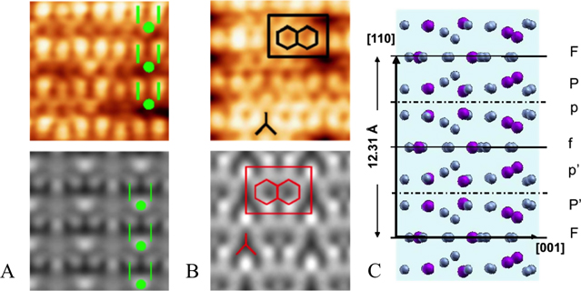
Figure 8. Top row: STM images of the Al Cu
Cu (110) surface showing the two puckered planes identified across terraces. Bottom row: simulated STM images obtained at V
 = +0.5 V for the PP (a) and PF (b) models. (c) Representation of the bulk structure along the [110] direction [59]. (Reprinted figure 8(a), (b) with permission from [59]. Copyright (2010) by the American Physical Society.)
Download figure:
Standard image High-resolution imageExperimental results (XPS, STM, LEED, STS) coupled with DFT calculations lead to the conclusion that two types of surface layers coexist across atomically flat terraces. Both types can be related to bulk planes (see figure 8). These terminations labelled PP and PF correspond respectively to puckered layers situated above another puckered layer or above a flat layer in the structural model. The simulated STM images are in reasonable agreement with experimental images and replicate the observed bias dependence. The greater stability of PP and PF compared to F layers is also supported by surface-energy calculations [59]. The calculated surface relaxations of both terminations remain minimal  . The DOS close to the Fermi level exhibits a pseudogap along with two maxima associated with the Cu p and d states hybridized with Al p states. As for most CMA (periodic and aperiodic) surfaces, the densest Al-rich atomic planes resulting from a bulk truncation at the largest interlayer spacing are preferred surface terminations [59].
Although the agreement between the experimental data and simulated results is reasonable, the presence of many surface defects and a tendency towards Al segregation has been highlighted experimentally (XPS, STM). This must be linked to the presence of points defects highlighted recently by ab initio calculations [60]: in Cu-rich alloys, the dominant defects are Cu antisites on the Al sublattice with Wyckoff position 4e (inner tetrahedron), while in Al-rich compounds, they are Al antisites on the Cu sublattice with Wyckoff position 4e (inner tetrahedron). This is also in line with previous results reported in α-Cu-Al solid solutions containing 9–16 at.% Al [61–64] and with DFT calculations on the segregation of Cu atoms embedded in an Al matrix, showing that the presence of copper in the topmost layer is energetically unfavourable [65]. The detailed understanding of the refined surface structure is challenging, and cannot be explained simply by a pure aluminum surface termination, since bias dependence is observed in STM images.
3.2. The (001) surface of the AlCo crystal


The Al Co
Co sample, of reduced structural complexity compared to the above-mentioned CMAs, represents an ideal system to determine the driving force responsible for the selection of specific planes as surface terminations. The (001) surface of this Hume–Rothery alloy has been investigated using an experimental and a theoretical approach. To minimize the surface free energy, several effects such as chemical surface segregation, surface reconstruction or specific plane selections could have been expected. LEED and angle-dependent XPS measurements indicate that the first two phenomena can be disregarded [66].
The unique step height measured on the surface corresponds to half the (001) lattice plane distance. Hence, between the two different layers stacked along the (001) direction (either pure Al or containing both Al and Co atoms), only one will be present as surface terminations. When combined, relative surface energy calculations, measured and calculated STM images and electronic structure give many arguments to correlate the surface structure with pure Al bulk planes (see figure 9). Moreover, relative surface energies of additional models with different chemical compositions and density demonstrate that the presence of surface Co atoms is disadvantageous even for denser topmost layer. The calculations of the local DOS for both bulk planes indicate a strong mixing of Al sp and Co d states, characteristic of covalent character of the Al-Co bonds. From the shape of the electron density isosurface, enhanced charge density distribution can indeed be identified between Al-Co atoms but also along  bonds between antiprisms (clusters used to describe the
  bulk structure (see figure 9)) [66]. While shallower compare to the bulk, the pseudogap is maintained up to the Al-rich surface layer.
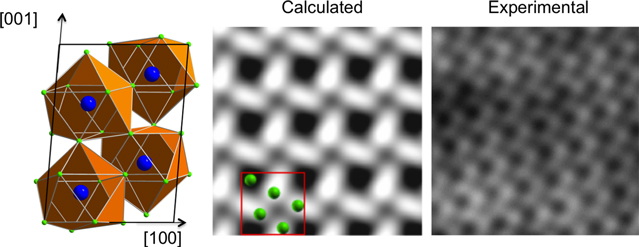
Figure 9. (Left) Bulk structure of the Al Co
Co crystal where the single-capped square antiprismatic clusters have been highlighted. The large (small) spheres correspond to Co (Al) atoms. (Middle) STM image of the (001) surface simulated at 1.3 V for an Al-rich plane. (Right) Experimental STM images recorded on the Al
 Co
Co (001) surface for V
 = −1.3 V, I
 = 0.36 nA [66]. (Reprinted figure with permission from [66]. Copyright 2011 American Chemical Society.)
Download figure:
Standard image High-resolution imageConsequently, the selection of a dense Al-rich layer as a surface termination resulting from a bulk truncation is mainly driven by the low elemental surface energy of Al compared to Co atoms and by covalent character of Al-Al bonding between the antiprisms present in the Al Co
Co bulk structure [66].
3.3. The (001) surface of the AlCu crystal

A system with a reduced structural complexity (smaller unit cell) is not synonymous with a less complex system as illustrated by the investigation of the Al Cu(001) surface. This alloy has been originally studied by Friauf [67] who described it as a tetragonal crystal that belongs to the I4 /mcm space group with a unit cell of 12 atoms (8 Al and 4 Cu atoms) and parameters a = b = 6.04 Å and c = 4.86 Å. Since then, several studies have revisited this phase leading to different models used to describe the structure of the Al
 Cu crystal. Using a chemical bonding approach, Grin et al [68] have demonstrated the existence of three types of covalent interactions in this intermetallic, although the Al
 Cu compound is usually considered as a full electron-like system.
Among these interactions, two of them labelled d1 and d2 (Al-Al bonds) in figure 10 are of particular interest. Indeed, they lead to a better understanding of the crystal description proposed by Nowotny and Shubert as interpenetrating graphite-like aluminum 6 nets with copper atoms positioned in the channels between the nets [70]. Figure 10(a) represents the Al
 Cu bulk structure without Cu atoms. The closest Al-Al distances within (001) planes is denoted d1, while d2 corresponds to the closest interlayer Al-Al distances. Figure 10(b) shows only one set of graphite-like Al nets parallel to the [110] direction and separated by d
 (equal to 1/2
  ). The surface preparation of the Al
 Cu(001) surface consists of cycles of sputtering and annealing to 753 K. After several cycles, the LEED pattern presented in figure 10(c) exhibits a
  surface reconstruction with two domains perpendicular to each other. This reconstruction is only visible when the sample temperature is below 373 K. STM measurements present terraces separated by a single step height of c/2 (2.4 Å), a value corresponding to two consecutive Al or Cu layers in the bulk. As seen in figure 10(d), higher resolution STM images reveal atomic rows separated by different widths (M = 13 Å, L = 17 Å and less often 21 Å) distributed in two mutually orthogonal domains. The rows originate from vacancies spaced by S = 8.5 Å propagating in the [110] and [
 0] directions. To interpret these specific values (L, M, S), several models have been developed. Considering angle-resolved XPS measurements (no surface segregation detected), the density of pure Al versus pure Cu plane in the Al
 Cu bulk structure and surface energy calculations of both elements, a surface model has been proposed based on incomplete pure Al bulk planes [69]. This selection is also consistent with the surface terminations of a large number of Al-based intermetallics which result from the selection of dense Al-rich bulk planes (see previous sections).
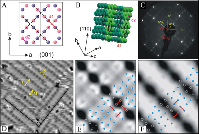
Figure 10. (a) View of the (001) plane without Cu atoms. (b) Graphite-like aluminium planes parallel to the [110] direction. (c) LEED pattern recorded for the Al Cu(001) surface revealing the
  surface reconstruction with two domains rotated from each other by
  . (d) 20 nm × 20 nm high resolution STM image showing the atomic rows separated by two main spacings (L and M) and the two domains rotated by 90
 from each other. The spacing S between two consecutive vacancies (highlighted as diamonds) is measured at 8.5 Å. Constant current simulated STM images using (e) 17 Å and (f) 13 Å wide row surface model at a contour of ρ = 3.7 10
 e/Å
e/Å and ρ = 7.2 10
 e/Å
e/Å respectively [69]. (Reprinted figure with permission from [69]. Copyright (2012) by the American Physical Society.)
Download figure:
Standard image High-resolution imageUsing ab initio calculations, it has been shown that the formation energy of Al vacancies at the surface (i.e. of reduced coordination) is lower than in the bulk. Interestingly, the formation energy of surface Al vacancies is the lowest for Al atoms separated by the distance d1 (energy increasing with increasing Al-Al separation). The surface vacancies labeled S in figure 10(d) are associated with pairs of missing Al–Al atoms (every other pair), the latter belonging to aluminum 6 nets. This distribution of vacancies along both sets of graphite-like nets leads to the
  surface reconstruction with two domains at 90
 . The widths of the L and M rows are now linked to interplanar Al 6
 distances, hence they are equal to 3 × d
 and 4 × d
 . It is important to note that the formation of vacancy pairs avoids breaking d1 covalent bonds at the surface. This model can also explain the alignment (shift) of vacancies perpendicularly to rows of width L (width M) as seen in figures 10(e)–(f).
An interesting surface phenomenon is the dynamical aspect of the atomic rows, even at 300 K. Between two consecutive scans of the same region, STM images reveal a different local structure with clear changes in the row directions and widths (M modified to L and vice versa). The surface dynamics is inhibited if the crystal is maintained at 60 K. From the experimental results and the calculations performed, it has been concluded that the surface structure is energetically rather than kinetically stabilized.
To further interpret our observations, the vibrational and entropic contributions have been estimated based on a simple model. The results indicate that both factors contribute to the stabilization of this surface reconstruction as they participate in a lowering of the total energy of the system. It is important to note that the presence of a pseudogap at the Al Cu(001) surface has been confirmed by experimental measurements and ab initio calculations [69]. The study demonstrates the considerable role of Al–Al covalent-like interactions and graphite-like Al nets on the surface structure.
4. Thin films, alloy surfaces and reactivity of CMA surfaces
As presented above, several CMA surfaces of various complexity and chemistry are now electronically and structurally well characterized. As will be discussed in the next sections, some of them have been used as templates for adsorption experiments, thin film growth and formation of surface alloys. The following section will also deal with recent work carried out on the chemical reactivity of specific CMA surfaces.
4.1. Ag and Pd adsorption on the - AlPdMn pseudo-tenfold surface


The growth of Ag and Pd thin films on the p-10f surface of the  -Al
-Al Pd
Pd Mn
Mn orthorhombic phase has been studied by STM. It was found that the Pd adatoms readily form some metal particles with no ordered structure upon room temperature deposition [71]. Their average size increases slightly with film thickness, up to 7 monolayers (ML). The local electronic structure of the Pd thin film has been studied by STS and appears to be particle-size dependent, with a possible transition from non-metal to metal with increasing particle size. In the case of Ag thin films, STM shows the formation of hexagonal islands. These have fcc symmetry and pyramid-like multilayer stacking along the [111] direction [72]. They can adopt two different orientations with respect to the substrate, rotated by 12
 around their [111] growth axis. The orientation relationship of the nanocrystallites with respect to the substrate can be explained by the fact that the densely packed rows of the adsorbate tend to be aligned along the densely packed rows of the substrate surface plane [73].
4.2. Pb adsorption on the AlCo(100) surface


The growth of Pb adatoms on the i-Al Pd
Pd Mn
Mn surface leads to the formation of a pseudomorphic mono-element ultra thin film. Upon initial deposition, Pb atoms adsorb preferentially at specific sites on the surface, which leads to the formation of pentagonal Pb islands across terraces (heterogeneous nucleation). With increasing coverage, the density of these islands increases until they interconnect to form an aperiodic network. The interstices of this Pb skeleton are then filled by additional impinging Pb atoms. The structure of the resulting dense film is then described by a Penrose P1 tiling [74]. In the case of Pb adsorption on the decagonal Al-Ni-Co quasicrystal surface, the growth is different and proceeds with the lateral expansion of irregularly shaped two dimensional Pb islands. When completed, the dense Pb monolayer is also quasiperiodically ordered, i.e. this is a pseudomorphic growth [75]. The adsorption of Pb atoms on the pseudo-tenfold Al
 Co
Co (100) surface provides an opportunity to study the adsorption on a surface that is structurally intermediate to elemental metals and quasicrystals. This work is also important for assessing the influence of clusters present within the topmost surface layers on the adsorbate growth mode.
The adsorption of Pb on the Al Co
Co (100) surface has been characterized by both experimental measurements (STM, XPS, LEED) at 300 K and 573 K and ab initio calculations. At low coverage, STM images reveal a significant mobility of Pb atoms at 300 K. Although very mobile, several adatoms already decorate preferentially specific sites of the substrate. At this stage, the resolution of the substrate is sufficient to identify the nucleation site. Individual Pb adatoms that appear as bright protrusions in the images are located on top of one set of bipentagonal motifs. This is also supported by the distances measured between individual atoms, which correspond to multiples of the lattice parameters along the b- and the c-axis. Hence, Pb atoms deposited on this substrate are not randomly distributed. Upon increasing coverage, Pb atoms self-assembled into one dimensional features aligned along the [010] direction. This pronounced row structure shown in figure 11(a) has an average height of 2.1 ± 0.1 Å. With the first monolayer completed and regardless of subsequent exposures, there was no sign of the onset of the second layer growth. Diffraction patterns and calculated Fast Fourier transform of STM images indicate a pseudomorphic growth mode, i.e. similar behaviour as on quasicrystal surfaces.
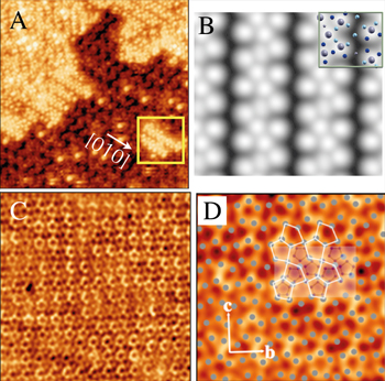
Figure 11. (a) 20 nm × 20 nm high resolution STM image showing the Al Co
Co (100) surface after deposition of 0.38 monolayer equivalent (MLE) Pb adatoms at 300 K. The frame indicates the Pb row structure that initially propagates along the [010] direction. (b) Simulated STM image (V = −0.5 V) of the Pb rows aligned along the [010] direction at a coverage of 0.4 MLE. The unit cell has been highlighted. The largest spheres correspond to Pb adatoms while the others are Al atoms belonging to the protruding (dark blue/black) or buried (light blue/small grey spheres) bipentagonal motifs. The two Al glue atoms are represented by the smallest spheres (light gray). (c) 18 nm × 18 nm STM image obtained for a complete Pb ML deposited at 573 K on the surface. The structure is composed of irregularly shaped pentagonal features. (d) Tiling using irregular pentagons of a region (7.25 nm × 7.25 nm) extracted from the STM image presented in (c). The surface structure can be described as interconnected bipentagonal motifs (see white pentagons). To analyse the ML formed, the structure of the P plane (bipentagonal motifs pointing in two directions and glue atoms) has been superimposed on the Pb structure [76]. (Figures reproduced from [76], © IOP Publishing
  Deutsche Physikalische Gesellschaft. CC BY-NC-SA.)
Download figure:
Standard image High-resolution imageTo analyse the initial growth mode of Pb adatoms on this surface, relative adsorption energies have been calculated for different models of the substrate [77]. Among the different possibilities considered, the surface termination composed of only Al atoms determined by dynamical LEED analysis [47] (see section 2.6) reproduces the initial nucleation site and the Pb row structures observed experimentally. The simulated images shown in figure 11(b) are indeed in good agreement with experimental findings. This computational approach not only allows a better understanding of the Pb adsorption on this complex surface but also indirectly validates the surface model determined by diffraction technique.
As shown in figure 11(c), the adsorption of Pb on a sample kept at 573 K greatly improves the quality of the film deposited and therefore the associated resolution of STM images. The surface plane is mainly composed of pentagonal atomic arrangements distributed on a periodic network. The better atomic ordering within the monolayer is also reflected in the (1 × 1) LEED pattern of quality clearly superior to that obtained for deposition at 300 K. To analyse the structure of the Pb monolayer, a tiling has been derived by associating each bright contrast within one unit cell to an adatom. The resulting arrangement, distributed periodically across the surface plane (figure 11(d)), leads to an interpretation of the thin film structure as being composed of connected bipentagonal motifs. This atomic configuration is reminiscent of the arrangement of Al atoms within the topmost termination of the substrate, which also consists of bipentagonal motifs but smaller in size. Although the positioning of the underneath bipentagonal motifs remains arbitrary, it stresses the influence of surface aggregates on the local atomic arrangement of the adsorbate. XPS analysis of the monolayer leads to a film density of 0.09 atom.Å . This value is greater than that established by associating a Pb atom to each high contrast in the STM images. Consequently, further experimental studies including dynamical LEED I(V) analysis would be necessary to validate the proposed superposition and to refine the film structural model.
The adsorption of Pb on the Al Co
Co (100) surface replicates the main trends observed on quasicrystal surfaces; heterogeneous nucleation, pseudomorphy, adatom mobility at 300 K and growth of additional layer inhibited. This study also demonstrates the dominant role of the adsorbate-substrate interaction via the surface clusters at the initial stages of the nucleation. Additional work is now required to investigate the chemical and physical properties of Pb monolayers of various structural complexity.
4.3. Bi adsorption on the AlCo(100) surface


As explained above, Pb adsorption on quasicrystals and on the Al Co
Co (100) surfaces result in the formation of pseudomorphic monolayers [74, 75, 78], coverage above which the onset of a second layer or island growth has not been observed. This is different from the adsorption of Bi on quasicrystal surfaces which leads to the formation of a pseudomorphic layer followed by the growth of nanocrystallites/islands of magic heights up to 5 ML. The latter possibly originate from quantum size effects arising from electronic confinement within the film thickness [79, 80]. The islands display a rotational epitaxial relationship with the underlying substrate [80, 81]. To understand how a complex but periodic intermetallic alloy surface will influence the growth mode, Bi adsorption on the Al
 Co
Co (100) surface has been studied.
Upon initial adsorption at 300 K, the highly mobile Bi adatoms tend to interconnect to form chains extending preferentially along the [010] direction (similar to the above Pb case). At 1 ML, the LEED pattern and the STM measurements indicate the formation of a Bi pseudomorphic layer. The latter remains stable up to 600 K. For 2.6 ML deposition, the islands exhibit three different specific heights with various shapes: S (0.68 ± 0.02)-irregularly shaped, M (0.93 ± 0.02)-resembling a truncated hexagon, and L (1.32 ± 0.03 nm)-either an elongated rectangle or resembling a truncated hexagon. The structure of bulk Bi is rhombohedric (space group  m). From a simple bulk truncation, the low index surfaces will exhibit a pseudosquare structure ((110) surface) and pseudohexagonal structures ((111) and (100) surfaces). Hence, these observations are interpreted as reflecting the pseudocubic (110) and hexagonal (111) orientation of the Bi islands normal to the surface. The thickness of the S and L (rectangular) islands match the thickness of two and four layers of Bi(110) with pseudosquare structure respectively. The M islands are understood as three layers of Bi(111), the first layer being in contact with the underlying
  (100) surface. This implies a reordering of the first Bi wetting layer, i.e. the adlayer-substrate interface. Then, the hexagonally shaped L islands could be associated with M islands with an additional (111) puckered plane on top. With increasing coverage, the growth mode proceeds in a layer-by-layer fashion with an evolution of the island height distribution towards the L value. Above 5 ML, the LEED patterns are interpreted as arising from 4 hexagonal domains of Bi(111), orientationally ordered with respect to the substrate. A diffuse ring in the diffraction pattern corresponds to remaining Bi(110) islands randomly oriented at the surface. The moiré pattern observed by STM on hexagonally shaped islands is induced by the island-substrate interface coincidence of lattices. A similar experiment performed at 57 K shows similar results with the exception of a higher fraction of L islands with (110) structure, i.e. the (111) structure is kinetically limited at low temperature (see figure 12). Upon annealing to room temperature, grain coalescence occurs and most of the film transforms from a pseudocubic to an hexagonal form [82]. Regarding the electronic structure of the M and L islands, STS measurements have been performed and reveal a dip in the DOS around the Fermi level. Such a minimum is not observed for the S islands. Compared to the spectra collected on the clean Al
 Co
Co (100) surface, additional peaks have been identified for each island-type, some of them already reported in previous work [83].
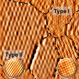
Figure 12. 60 nm × 60 nm tunnelling current image of 5 ML of Bi adatoms deposited on the Al Co
Co (100) surface and imaged at 57 K. The boundaries between the Bi(110) (Type I) and Bi(111) (Type II) structures are indicated by dashed lines. The two insets show atomic resolution images of the structures present in Type I and II domains [82]. (Figure adapted from [82]. Copyright (2012) by the American Physical Society.)
Download figure:
Standard image High-resolution imageIt has been demonstrated that Bi(110) and Bi(111) structures coexist between 1 and 5 ML from 57–300 K. To understand this delicate balance between both phases, ab initio calculations have been carried out. The results demonstrate a lower surface energy for free-standing Bi(111) layers compared to Bi(110) slabs of the same thickness [82]. In addition, an oscillating behaviour of the surface energy is observed for the Bi(110) structure with minima occurring for even numbers of layers. This bilayer predicted growth is in agreement with the STM measurements and earlier reports [84]. Consequently, the 'magic heights' of the observed Bi islands may result from a stabilization via layer-pairing to avoid dangling bonds rather than from quantum size effects.
Finally, oxygen adsorption experiments have been performed on the Al Co
Co (100) surface after dosing 2.6 ML of Bi adatoms. From STM observations, it has been found that protrusions, related to oxygen adatoms, are present mainly on the Bi pseudomorphic monolayer. Hence, after exposing the surface to more than 10000 L of O
 , the Bi pseudomorphic monolayer appears more reactive than the S-, M- and L-type islands [82]. Similar observations have also been reported when depositing C
 molecules on Bi allotropes grown on the i-Al-Pd-Mn quasicrystal. The size and the number of hexagonal C
 domains obtained on the aperiodic pseudomorphic Bi monolayer indicate a limited diffusion of the molecules across terraces. This originates from a molecule-substrate interaction which appears stronger on the Bi pseudomorphic monolayer than on the remaining Bi allotropes, i.e. pseudocubic and hexagonal Bi islands [81].
4.4. Formation of surface alloys
As demonstrated in the previous section, the formation of pseudomorphic thin films has been achieved on several systems, most of them characterized by a heterogeneous nucleation. Among the different attempts to achieve pseudomorphic growth, the adsorption of Cu atoms has led to the formation of surface alloys on different systems. It has been shown using STM and LEED techniques that Cu adatoms deposited on the fivefold and twofold i-Al Pd
Pd Mn
Mn surface yields quasiperiodic structures [86, 87]. However, five-rotational domains of (110)-orientated β-Al(Cu, Fe) phase are obtained for 8 ML Cu atoms adsorbed on the fivefold i-Al-Cu-Fe surface [88]. Annealing a 20 ML thick film leads to the formation of five domains of γ-Al
 Cu
Cu exposing the (110) surface. The latter phase had been previously reported when annealing a thick Cu film adsorbed on the fivefold i-Al
 Pd
Pd Mn
Mn surface to 623 K [89] and by annealing Al thin films deposited on a Cu(111) surface [90]. Complementary to these studies, the adsorption of Cu atoms has been carried out on the Al
 Co
Co (100) surface for different coverages and temperature regimes [85]. The highly symmetric clusters present at the surface introduce an extra physical length scale in addition to the lattice dimensions. Hence, it is of interest to use this template of intermediate complexity to highlight if the clusters have any influence on the Cu growth mode. One goal of this study is also to test the possibility of forming pseudomorphic monolayer and surface alloys of CMA type (decagonal Al–Cu–Co quasicrystalline surface alloy for instance) depending on the adsorption conditions.
A multi-technique approach using STM, LEED, XPS and XPD methods coupled with numerical simulations (SSC simulations) has been necessary given the complexity of the system. From 300 to 573 K, the growth of Cu adatoms is pseudomorphic on the Al Co
Co (100) surface up to 1 monolayer. The p-10f symmetry of the monolayer is confirmed by the LEED patterns and calculated fast Fourier transforms of STM images. In the submonolayer regime, the density of Cu islands varies drastically with the sample temperature. Compared to room temperature deposition, the number of individual islands is drastically reduced (coalescence occurring), hence reflecting a greater mobility of the adsorbate at that temperature. At 573 K, the growth mode proceeds via the coalescence of irregularly shaped islands and the step edges are now well decorated. Photoemission measurements indicate an Al enrichment at the surface compared to Co atoms (demixing) and an enhanced diffusion of Cu adatoms within the substrate at 473 K. Hence, the pseudomorphic monolayer is likely to contain both Al and Co atoms in addition to Cu adatoms, in contrast to Cu adsorption on the fivefold surface of the i-Al
 Pd
Pd Mn
Mn quasicrystal surface where Cu grows in a layer-by-layer manner with no intermixing. Above 2 ML, LEED, XPS and XPD measurements suggest the formation of a β-Al(Cu, Co) phase with two (110) domains rotated by approximately 72
 from each other. XPS measurements indicate a phase separation with an Al (Co) enrichment (depletion) at the near-surface region upon Cu deposition. SSC simulations reproduce the experimental observations.
Above 7.5 ML and at 473 K, the β-Al(Cu, Co) phase is replaced by a new phase as demonstrated by the additional weaker diffraction spots present in the LEED pattern (see figure 13(a)). The reciprocal space unit cell can be subdivided into 3 × 3 sub-units with two domains orientated from each other by 72 . The lattice parameter of this new unit cell can be related to the lattice parameters of the (110) surface of the γ-Al
 Cu
Cu phase. The corresponding high resolution STM image displayed in figure 13(b) and taken on a single domain exhibits a structure similar to that obtained on the γ-Al
 Cu
Cu (110) single crystal surface (see figure 8 for a comparison) [59]. Figures 13(c), (e) corresponds to SSC simulations performed for the Al 2s and Cu 2p core levels. It has been determined from LEED and STM measurements that two Al
 Cu
Cu (110) domains coexist at the surface. Hence, SSC pattern in figure 13(d) has been generated by additive superposition of the SSC simulation displayed in figure 13(e) with itself rotated by 72
 . When comparing the latter to the experimental XPD pattern (figure 13(f)), the main intensities are indeed well reproduced in the SSC simulations. Consistent with the formation of the γ-phase, the binding energy of the Al 2s shifts gradually upon Cu adsorption to reach the value measured on the Al
 Cu
Cu (110) crystal surface (binding energy of Cu 2p core level also in agreement with this phase) [85].
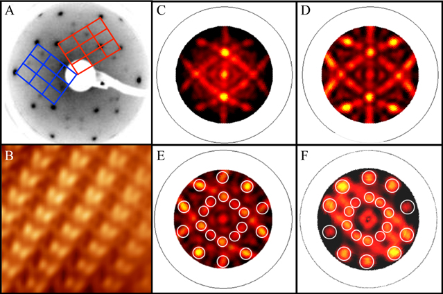
Figure 13. (a) LEED pattern (60 eV) obtained for 10 ML Cu deposition with the sample held at 473 K. The unit cell of the two domains are outlined. (b) 6 nm × 6 nm Fourier-filtered STM image showing the atomic structure of the γ-Al Cu
Cu phase. SSC simulations for (c) the Al 2s (E
 = 1370 eV) and (d) the Cu 2p (E
 = 1166 eV) core levels. (e) SSC pattern generated by additive superposition of the SSC simulation displayed in (b) with itself rotated by 72
 . (f) XPD pattern obtained for the Cu 2p core level after 15 ML coverage [85]. (Figures reproduced from [85], © IOP Publishing. Reproduced with permission. All rights reserved.)
Download figure:
Standard image High-resolution imageA careful analysis of the domain orientations for both β and γ phases demonstrates that the bipentagonal motifs present on the clean Al Co
Co (100) surface dictate the growth orientation of these domains. These bipentagonal motifs represent either the top or bottom caps of the elementary pentagonal bipyramid clusters. Finally, the formation of the Al
 Cu
Cu phase seems independent of the initial structural complexity and bulk composition of the substrate as long as a critical amount of Al and Cu film thickness are reached.
4.5. Surface reactivity
CMAs are promising candidates as stable, active and selective catalysts. Following a knowledge-based approach, a number of selected intermetallics have been tested over the last few years. The first study may have been the one on the Pd-Ga intermetallic compounds for the semi-hydrogenation of acetylene, which is an important industrial reaction involved in the production of polyethylene [92, 93]. As already mentioned in section 2.7, the Al Fe
Fe intermetallic compound has been identified as a low cost alternative for palladium in heterogeneous hydrogenation, towards both acetylene [53] and butadiene [94]. A similar behaviour has been measured for Al
 Co
Co in the case of the semi-hydrogenation of acetylene [53].
Some insights on the mechanisms at the origin of the specific reactivity of Al-based complex intermetallic compounds have been revealed by recent theoretical works by Krajčí and Hafner [95–97]. They focused mainly on the reactivity (i) of the pseudo-tenfold Al Co
Co (100) surface, using a surface model
5
which is built by theoretical cleavage, and (ii) of the pseudo-fivefold surfaces of the isostructural compounds AlPd and GaPd (B20 structure, FeSi-type) [95–97]. For all these compounds, they found the same type of reaction path. Reactants (H
(100) surface, using a surface model
5
which is built by theoretical cleavage, and (ii) of the pseudo-fivefold surfaces of the isostructural compounds AlPd and GaPd (B20 structure, FeSi-type) [95–97]. For all these compounds, they found the same type of reaction path. Reactants (H and C
and C H
H ) are adsorbed on the surface: H
 is adsorbed on a protruding transition metal atom, while the C
 H
H molecule is adsorbed on an Al-Al (or Ga-Ga) bridge position, close to a transition metal atom, the carbon atoms of the molecule forming di-σ bonds with surface aluminum atoms. In these studies, the active site has been shown to be not localized exactly on the transition metal atom, but it is slightly shifted to involve a priori non active surface aluminum atoms. Hydrogen atoms, produced by the dissociation of the H
 molecule, diffuse on the surface to reach the C
 H
H molecule and gradually transform C
 H
H into C
 H
H . The catalytic activity of the semi-hydrogenation is not controlled by the dissociation and mobility of hydrogen, but rather by the binding of hydrogen atoms to C
 H
H or C
or C H
H (see table 1 for the activation energies). The selectivity of the semi-hydrogenation depends on the activation energy
  of the binding of an additional hydrogen atom on the C
 H
H molecule and on the desorption energy
  of the C
 H
H molecule. It is interesting to notice that
  is almost
  lower than
  in the case of Pd(111) and Pd-Ag/Pd(111), while
  for complex intermetallics used as catalysts. This may explain the high selectivity of Al
 Co
Co (100) and PdAl(120) catalysts compared to the selectivity of simple metals and alloys.
Table 1.
Activation energies ( , in
, in  ) of a few elemental steps involved in the hydrogenation of acetylene and desorption energy
  , in
, in  ) of the C
 H
H molecule.

|

|

|

|
Reference | |
|---|---|---|---|---|---|
C H H
 C C H H
|
C H H
 C C H H
|
C H H
 C C H H
|
C H H
|
||
| Pd(111) | 66 | 85 | 72 | 82 | [98] |
| 62 | 78 | 72 | 82 | [99] | |
| 66 | 74 | 72 | 82 | [100] | |
| Pd-Ag/Pd(111) | 66 | 10 | 61 | 70 | [100] |
Al Co Co (100) (100) |
63 | 61 | 80 | 51 to 71 | [95] |
| depending on | |||||
| co-adsorbates | |||||
| PdAl(120) | 51 | 71 | 56 | 10 to 45 | [96] |
| depending on | |||||
| co-adsorbates | |||||
| PdGa(210) | 61 | 70 | 59 | 45 | [97] |
In the case of Al Fe
Fe , the active role of the intermetallic surface has been tested experimentally, by reductive (H
 ) or oxidative (O
 ) treatments [53]. While no drastic modification in the activity was found after the reductive treatment, the activity and selectivity dropped after treating the catalyst in
  at 473 K. The interaction of oxygen with these metallic surfaces appears crucial in the detailed understanding of the reactivity. To this end, oxygen adsorption studies have been carried out on the Al
 Co
Co (001) and o-Al
 Co
Co (100) surfaces [91, 101]. These surface structures have been determined in both cases to be dense pure aluminum surfaces (see sections 2.6 and 3.2). The most stable adsorption sites (atomic oxygen adsorption) have been identified to be specific bridge sites for Al
 Co
Co (001) and specific three fold hollow sites for o-Al
 Co
Co (100). Both sites are located far away from the closest cobalt atom (≃3.9 Å for Al
 Co
Co (001) and ≃5.5 Å for o-Al
 Co
Co (100)), while the closest Al-O distance varies in the two surfaces: it is 1.75 Å for the Al
 Co
Co (001) surface, while it is 1.85 Å for the o-Al
 Co
Co (100) surface. The distance 1.75 Å corresponds to the Al-O distances found for atomic oxygen adsorption on a surface vacancy site in Al(111) (1.73 Å [102]). The distance 1.85 Å corresponds to the Al-O distances found for atomic oxygen adsorption on Al(111) (1.84 Å [102]) and to the Al-O distances in Al
 O
O (1.86 Å [103]). From the calculated electronic local DOS and charge density distribution shown in figure 14, it appears that Al-O bonding has a covalent character with hybridization occurring between O sp and Al sp states. In both cases, important relaxations are noticeable for aluminum surface atoms when the adsorbate lies initially in a less stable fourfold or fivefold site. In the case of atomic oxygen adsorption on Al
 Co
Co (001), these results have been shown to be in reasonable agreement with the experimental observations (figure 14). The bright protrusions observed experimentally (motif 'c' in figure 14) may correspond to molecular oxygen, while motifs 'a' and 'b' could be due to atomic oxygen adsorption (see corresponding simulated STM images on figure 14).

Figure 14. (a) Representation (slice cuts) of the charge density distribution prior and after oxygen adsorption. (b) 9.6 nm × 12.1 nm STM image of the Al Co
Co (001) surface after 0.5 L O
 dosage. (c-d) Simulated STM images with atomic oxygen adsorbed on the two most energetically favourable bridge sites. The red (grey) arrows point to the adsorbed oxygen atom [91]. (Figures reproduced from [91] © IOP Publishing. Reproduced with permission. All rights reserved).
Download figure:
Standard image High-resolution image
Table 2. Summary of main systems reported in this topical review.
| Systems | Techniques used | Surface termination | Adsorbates used |
|---|---|---|---|
| ξ'-Al-Pd-Mn (010) [26, 27] | LEED, RHEED, XPS, STM | incomplete puckered bulk layer; presence of Al decagonal rings related to pseudo-Mackay clusters | Ag, Pd [71–73] |
T-Al (Mn, Pd) (010) [30] (Mn, Pd) (010) [30] |
LEED, XPD, SSC, XPS, STM, UPS, DFT | puckered bulk layer (P2-type) containing both Al and TM elements | Pb [117] |
μ-Al Mn (001) [35] Mn (001) [35] |
LEED, XPS, XPD, SSC | bulk truncated surface termination; six-fold surface | N/A |
Al (Cr,Fe) (100) [37] (Cr,Fe) (100) [37] |
LEED, STM | two terminations present at the surface; results consistent with the bulk model | O [118] [118] |
Al (Cr,Fe) (010) [37] (Cr,Fe) (010) [37] |
LEED, STM | pseudo-decagonal symmetry observed in LEED; microfacetting of the surface at  C, no STM images available C, no STM images available |
O [118] [118] |
Y-Al Ni Ni Co Co (100) [39, 43] (100) [39, 43] |
LEED, STM, STS | three surface terminations identified related to the densest bulk planes, three types of surface reconstructions identified; electronic states localized on equivalent topographic features | N/A |
Al Co Co (100) [46–49] (100) [46–49] |
LEED I(V), XPD, SSC, XPS, STM, DFT, UPS | two experimental models exclude protruding Co atoms and exhibit distinct surface density; one model from simulated cleavage leads to incomplete puckered bulk layer with the preservation of intact clusters | Cu [85], Bi [82], Pb [76, 77], O [119], H [119], H and C and C H H [95] [95] |
Al Fe Fe (010) [53, 55] (010) [53, 55] |
LEED, XPS, STM, UPS, DFT | incomplete puckered bulk layer; corrugated surface; preservation of intact clusters | butadiene [94],  and and  [53] [53] |
2-f and p-10f  [57] [57] |
XPS, STM, Mass spectrometry | Zn surface segregation above  C; no evidence of a terrace-step morphology C; no evidence of a terrace-step morphology |
O [57] [57] |
Al Cu Cu (110) [59] (110) [59] |
LEED, XPS, STM, STS, UPS, DFT | two types of terminations related to bulk puckered layers; small surface segregation | O [119] [119] |
Al Co Co (001) [66] (001) [66] |
LEED, UPS, XPS, STM, DFT | surface terminated at pure Al bulk plane | O [91, 119] [91, 119] |
Al Cu(001) [69] Cu(001) [69] |
LEED, UPS, XPS, STM, STS, DFT |
 reconstruction with two domains rotated from each other by 90 reconstruction with two domains rotated from each other by 90
|
N/A |
5. Discussions and conclusions
Surfaces of quasicrystals are usually laterally unreconstructed and the topmost surface layers are considered as bulk-terminated [21–23, 104]. Additional phenomena have been observed mainly for twofold surfaces of decagonal quasicrystals where facetting of the (12110) surface and variation of the surface periodicity along the [10000] have been reported for decagonal phases of various compositions [40–42] (see section 2.5). The Y-Al-Ni-Co(100) surface (related to a twofold decagonal surface) is also a system where local reconstructions have been identified [39]. For the remaining approximants studied so far, the unit mesh of terrace-terminated surfaces corresponds usually to what would be obtained by a simple truncation of the bulk lattice. Although unreconstructed, the surface terminations are often incomplete and/or present structural imperfections [26, 30, 55, 59]. For several systems reported here, the bulk structure can be described in the direction perpendicular to the surface as a stacking of flat and puckered layers following particular sequences of appearance. Apart from the sixfold  -Al
-Al Mn(001) surface where flat layers are preferred [35], the topmost layers of pseudo-tenfold surfaces are usually associated with puckered layers present in the bulk (ξ'-Al-Pd-Mn, T-Al
 (Mn, Pd), Al
 Co
Co , and Al
 Fe
Fe crystals). This is also the case for the Al
 Cu
Cu (110) surface [59]. The selection of Al-rich puckered layers as surface terminations may be dictated by their atomic density which is the highest among the bulk planes in the model. The chemical bonding network present within the bulk can modify the final structure of these puckered layers when exposed at the surface (reconstruction, reduction of the atomic density,...) [49, 55, 66, 69]. This selection implies that the hemispherical part of the cluster is exposed at the surface. Consequently, one can speculate that it is more energetically favorable to avoid equatorially truncated elementary clusters.
The creation of flat terraces on Al-based quasicrystals implies that elementary clusters (Bergman and pseudo-Mackay) are dissected at different heights. Although incomplete, these cut entities remain apparently stable within the surface terminations. A different behaviour has been reported for the Al Fe
Fe (010) surface where truncated pentagonal bi-pyramid clusters will be absent within the surface layer [55]. A similar behaviour is predicted by simulated cleavage of the Al
 Co
Co (100) surface [49], although not observed experimentally under the temperature range investigated [46, 47].
The Al TM
TM approximants are clear examples where a three-dimensional description of the bulk structure using highly symmetric clusters [105] is more appropriate than a description based on a stacking of two-dimensional atomic layers. This concept is further supported by quantum chemical calculations highlighting the existence of a three-dimensional chemical bonding network within the materials [50]. As discussed in section 2.7, the covalent-like bonding within the sample leads to a corrugated surface structure with isolated Al-TM ensembles. It is foreseen that similar chemical properties will be present in other binary CMA phases. These features correspond to the criteria required to fulfil the site isolation concept proposed by Kovnir et al [54]. Within this concept, the isolated atomic complex will limit the adsorption geometries of the reactants, hence reducing the possible reaction products and the covalent bonding should stabilize the desired geometry under reaction conditions. Despite the recent patents and studies [53, 94, 106], information related to CMA and heterogeneous catalysis remain scarce but this field should blossom in the coming years.
As mentioned in the introduction, quasicrystals exhibit a pseudogap which is preserved at the surface. From ab initio calculations and experimental evidence, such a reduction of the electronic DOS is also present on periodic CMA surfaces with a pseudogap depth varying with the chemical content of transition metal elements and the structure of the phases [30, 49, 59, 107]. In addition to the well-established parabolic pseudogap, calculations have demonstrated that the DOS of quasicrystal and approximant systems should be dominated by a set of spiky peaks near the Fermi level [108]. The origin (densely distributed dispersionless bands, calculation methods,...) and the existence of these fine spiky features along with their role in the transport properties have been a matter of debate from early days [11, 108–112]. With the hope of shedding some light on the issues, high-resolution ultraviolet photoemission spectroscopy measurements were initiated on quasicrystal surfaces scratched under ultra high vacuum conditions. The decrease of the spectral intensity measured near the Fermi level has been assigned to the pseudogap. However, the spikiness of the DOS was not to be seen with a system resolution of 6 meV [113]. On the other hand, the preparation used in this study would not have led to a quasicrystal surface. A similar conclusion has been drawn from tunnelling and point contact measurements carried out at low temperature on a series of quasicrystalline alloys [114]. As explained in section 2.5, new experimental evidence of the spiky DOS has emerged from high resolution STS measurements on the i-Al-Pd-Mn quasicrystal [115]. This work has been recently extended to other systems including approximant surfaces [107]. The results demonstrate that spatially and energetically localized features dominate the local DOS across several CMA surfaces. This spikiness disappears if the spectra are averaged over a large surface area. It is known that the magnitude of the electron localization influence drastically the electrical resistivity. This has been shown theoretically by the models proposed by Mizutani [111] and by Trambly de Laissardière et al [116]. Using STS measurements on a series of quasicrystal and approximant surfaces, Mäder et al could not outline a correlation between the depth of the surface pseudogap and the high electrical resistivity of the Al-based CMA materials [107]. However, their STS analysis has highlighted a relationship that exists between the bulk electrical resistivity of a CMA compound and the degree of spikiness of its DOS [107]. Finally, it is suggested that the interaction between valence electrons and the complex local atomic structure should influence the macroscopic measurable electrical resistivity [107].
Regarding thin film growth, similarities have been highlighted between quasiperiodic and approximant surfaces. The Ag adsorption studies reveal a comparable smooth growth at low coverage  on the d-Al-Ni-Co tenfold and
  -Al
-Al Pd
Pd Mn
Mn pseudo-tenfold surfaces [71]. For higher coverage (
 ML), Ag nanocrystals are formed irrespectively of the aperiodic and approximant surfaces chosen. The orientation of these hexagonal Ag islands is dictated by the rotational symmetry of the substrate selected. Regarding the adsorption of Pb adatoms, a common trend has emerged on both periodic and aperiodic Al-based surfaces. At submonolayer coverage, Pb adatoms remain highly mobile across the surface and the growth proceeds via heterogeneous nucleation. The growth mode is pseudomorphic and several preferential adsorption sites have been identified. The local Pb atomic arrangement also reflects the local features present on the templates [74, 76]. With the exception of Pb/T-Al
 (Mn,Pd) [117], the growth of a second layer has not been observed on the already deposited Pb pseudomorphic monolayer. This phenomenon is drastically different to what has been reported on the Al(111) surface [78] where a Frank–van der Merwe growth occurs. Similarly, the adsorption of Bi on quasicrystal and approximant surfaces results in the initial formation of a pseudomorphic monolayer. Above 1 ML coverage, the growth proceeds with the formation of Bi islands of different height, structure and orientation with respect to the substrate [79, 80, 82]. The selection of 'magic' Bi island heights has been ascribed to quantum size effects [79] and/or to a layer-pairing mechanism to avoid dangling bonds [82]. Finally, the growth of the γ-Al
 Cu
Cu phase has been achieved independently of the template structural complexity as long as the amount of Cu and Al and the annealing temperature were appropriate [85, 89, 90]. On quasicrystal surfaces, the domain orientation reflects the symmetry of the substrate [89] while it is governed by the cluster orientation in the Cu/Al
 Co
Co (100) system [85]. From these studies, it appears that the growth mode observed up to now on both approximant and quasicrystal surfaces are qualitatively similar.
With the handful of results presented in this review (see table 2 below for a summary of the different systems reported up to now), it is clear that the field of Al-based periodic CMA is still in its infancy. The continuous progress made in the crystal growth and the discovery of new complex systems will lead to new compounds with novel (combinations of) properties. From what has been gathered so far on periodic and quasiperiodic CMA systems [21–23, 104], the structural and electronic complexity present in the material is usually preserved at the crystal surfaces. Hence, the investigation of new intermetallic compound surfaces represent a fascinating opportunity to discover new surface phenomena.
Regarding the next challenges, work remains to be done in the quantitative structural determination of surfaces. To our knowledge, detailed atomic-scale structural information is still lacking for most CMA surfaces. Apart from a limited number of cases, the systematic characterization of the physical and chemical properties associated with the new surfaces and thin films formed should be also considered as one of the major tasks ahead. To conclude, we believe that the study of binary periodic CMA surfaces has opened up a new field of research which is of interest far beyond the community of scientists working on aperiodic systems [53, 94]. This bridging across communities is facilitated nowadays by the availability of centimetre-sized samples, by established and transferable surface preparations and by the presence of translational symmetry within the materials which allows ab initio type calculations to be introduced and routinely performed.
Acknowledgments
The Agence Nationale de la Recherche (Projet ANR-11-INTB-1001) is acknowledged for its financial support. Part of the work presented in this review is a result of the cooperation within the European C-MAC and was possible thanks to the access to HPC resources of the French institute IDRIS (Institut du Développement et des Ressources en Informatique Scientifique) under allocation 99642 made by GENCI (Grand Equipement National de Calcul Intensif).
Footnotes
- 1
The step height distribution is highly sensitive to the surface preparation used and may differ for short annealing treatment [27].
- 2
- 3
In the concept of 'cluster virtual bound states', TM clusters can trap valence electrons at some energies via a scattering mechanism. The stronger the effect of the localization by the cluster is and the more spherical the clusters are (icosahedron and dodecahedron for instance), the narrower the peaks present in the DOS will be [11].
- 4
It is important to note that a decent agreement has been also found between experimental and calculated STM images for a model where only protruding Co atoms have been removed. However, this model leads to a higher LEED R factor as described in [47].
- 5
The surface model used differs from the experimental observations when the surface is prepared by sputter-anneal cycles.