


Abstract
The development of organic printed electronics has been expanding to a variety of applications and is expected to bring innovations to our future life. Along with this trend, high performance organic materials with cost-efficient fabrication processes and specific features such as thin, light weight, bendable, and low power consumption are required. A variety of organic materials have been investigated in the development of this field. The basic guidelines for material design and the recent progress of polymer-based organic light-emitting diodes (OLEDs) and organic photovoltaic cells (OPVs) are reported.
Export citation and abstract BibTeX RIS

Content from this work may be used under the terms of the Creative Commons Attribution-NonCommercial-ShareAlike 3.0 licence. Any further distribution of this work must maintain attribution to the author(s) and the title of the work, journal citation and DOI.
1. Introduction
The development of organic printed electronics has been expanding to a variety of applications such as organic light-emitting diodes (OLEDs), organic photovoltaic cells (OPVs), electronic papers, wearable electronics and various sensors. It is expected that flexible, thin, and light-weight devices with cost-efficient productivity should bring innovation to our lives, which makes the research and development (R&D) in this area so competitive and global.
As self-emitting devices, OLEDs have features of fine image-quality, are ultra thin, and are light weight. They have become familiar to general consumers as they are equipped in smart phones such as Samsung's Galaxy series. Currently, an evaporation process is adopted for the mass production of OLEDs. Although this process is practical when used for the mass production of small and middle size OLED displays, it is still considered that some difficuties exist in the fabrication of large TV displays from technical and cost points of view.
We have been developing organic materials applicable to printed electronics based on conjugated polymer technology, because we expect the printing process to be essential for cost-competitive mass production of large sized TVs or flexible devices [1, 2].
Based on the R&D of OLEDs, we have also developed OPV materials whose working mechanism is the reverse to that of OLEDs. Recently, new applications or quality assurance projects have been announced by some companies. OPVs are still in the middle of development for use in materials, devices, modules, and fabrication processes. As with OLEDs, a printing process should be the key technology in the cost-efficient fabrication of large sized OPV modules, especially when it is combined with a roll-to-roll process. For these reasons, knowledge gained in the development of OLEDs can be effectively applied to OPV development.
In this article, material technologies in polymer OLEDs and OPVs are reviewed, from their development history to recent progress, including our experiences. A lot of materials used for organic printed electronics applications have been reported, and systematic reviews are frequently updated [3]. Such reports are very useful for grasping the characteristics of each conjugated polymer structure. On the other hand, organic electronics materials exhibit their performances as electric devices, hence their performance depends strongly on the combinations of materials, layer structures, process conditions in their fabrication, etc Theses circumstances make analysis and speculation complicated. Furthermore, device durability is also an important factor from the practical application perspective. The durability is governed by not only the chemical or physical stability of materials, but also by factors other than material properties. Therefore, parallel activities of basic analytical research and experimental screening are needed to promote material development. Such intrinsic circumstances in this field may lead to a situation where a few years (or more) are needed to find new materials and/or working mechanisms to bring them to completion for practical usage. We hope that these peculiarities of material research, strongly tied with device architecture and device fabrication processes, will be understood.
2. Polymer OLED
2.1. Development history and characteristics of polymer OLED materials
It was big news when Sony launched their eleven inch OLED-TV 'XEL-11' in 2007. Currently, Samsung's Galaxy series, equipped with OLED displays, are very popular. Although small or middle size displays have so far been the main products for OLEDs, the recent trends in OLED applications are shifting to large sized TVs or flexible/wearable display fields. As this trend develops, soluble light emitting materials have received lots of attention from a viewpoint of low-cost mass production and/or their applicability to flexible plastic substrates.
In 1989, a group from Cambridge University observed electroluminescence (EL) in a conjugated polymer [4]. Almost at the same time, we observed a similar phenomenon [5]. This was only a weak emission of 0.1% external quantum efficiency (EQE), and the device had a very short lifetime of a few minutes. After this finding, Sumitomo Chemical Co. Ltd, Covion in Germany, Dow Chemical in the US, and Cambridge Display Technology (CDT) in the UK started the energetic development of polymer OLED materials, as well as the optimization of device structures. As the results of over 20 years of R&D, high EQE of 5 ∼ 10%, and a long operating lifetime of over several tens of thousands hours have been achieved. Polymer OLEDs show not only red, green, and blue (RGB) emissions but also white color emissions, which are essential to various applications.
OLED emissive materials are categorized into a small molecule group and a polymer group as shown in figure 1. The polymer group is further classified into non-conjugated or conjugated subgroups. Dendritic compounds can be used as intermediate materials for the small molecule and polymer groups [6]. Currently, evaporation is practically the main process for OLEDs and small molecule are used in the panels. As detailed later, the trend of fabrication process is shifting from dry process (evaporation) to wet process. Along this trend, the development of solubilized small molecules was started with a sense of urgency. The introduction or replacement of substituent groups by small molecules is the main modification to acheive solubility in ink solvents. Figure 2 shows an example of how dithienylbenzothiadiazole derivatives were modified to become soluble materials [7]. As explained in the next section, small molecule OLEDs contain multilayer device architecture. Because of the requirement to form stacked layers, further modifications in chemical structures are needed, in addition to solubility. Although a lot of patents regarding this technology have been filed, solubilized small molecule OLEDs seem to still be under development for overcoming such requirements.
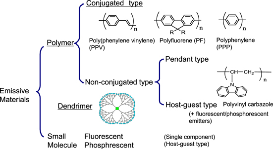
Figure 1. Schematic classification of polymer and dendrimer emissive materials.
Download figure:
Standard image High-resolution image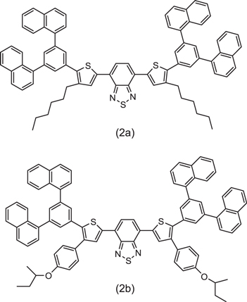
Figure 2. Solubilized emitters of dithienyl benzothiadiazole derivatives [7].
Download figure:
Standard image High-resolution imagePolymer OLED materials are readily soluble by ink solvents, and this results in appropriate materials for wet processes (printing processes) like inkjet, die-coating, etc which are considered to be appropriate for the fabrication of large sized OLED devices. Conjugated polymers, having sp2 carbons in the main chain, exhibit high electron and hole mobility originating from the delocalized π-electrons system. Many conjugated polymers with this characteristic have been reported as emissive materials in the visible region. Poly-phenylenvinylene (PPV) [4, 8], polyfluorene (PF) [9–12], and poly-p-phenylene (PPP) [13] are typical examples of conjugated polymer OLED materials.
Two types of non-conjugated polymer OLEDs, the pendant type and the host-guest blend type, have been developed to maximize device performance. In the former, functional units are attached to the non-conjugated backbone (polymer) and, in the latter, functional guests are doped into the host polymer. Of these non-conjugated types, polyvinylcarbazole (PVCz) is one of the typical polymers, and its optical and electrical properties were well-analyzed in the early stage of OLED developments [14, 15] where PVCz was used extensively as a host material. A fluorescent [16] or phosphorescent [17] host-guest polymer OLED containing PVCz in an emitting layer has also been reported. Furthermore, PVCz has been developed as a pendant type phosphorescent polymer where an iridium complex is incorporated in its side chain [18, 19]. As the fluorescent pendant version, triarylamine pendant type polymers have been studied, which offer the potential benefit of ease of synthesis compared to the conjugated type polymers [20]. Their OLED performance was evaluated as part of a mixture with the conjugated polymer in order to complement mutually insufficient functions. Owing to its ease of synthesis, non-conjugated type polymers have been used for basic studies of OLEDs rather than forpractical development because the independent controllability of emissive and carrier transporting functions can be relatively easily achieved by selecting suitable functional units.
Dendritic compounds are also useful for the printing process, particularly in combination with polymers. Dendrimers containing an iridium complex as the phosphorescent emitting core are known in red [21], green [22], and blue [23]. Polymer OLEDs utilizing conjugated polymers and red dendrimers already achieve a high enough performance for their practical usage [24].
The conjugated polymer system works well without a complex multilayer device structure, because the required functions are introduced into polymer chains by co-polymerization technology. A conjugated polymer consists of functional backbone units, electron affinity units, hole affinity units, or emissive units, as shown in figure 3. Emission color, which is one of the most important properties, is usually controlled by introducing an emissive unit to the polymer chains. Therefore, backbone units are generally selected from wide band gap structures. From this standpoint, polyfluorene [25–29] or polycarbazole [30], whose band gap is wide enough even for blue emission, are commonly used for a backbone structure. As a typical design of a polymer, fluorene-acene co-polymers are shown in table 1 [25]. Each acene unit was expected to emit RGB color; anthracene for blue, naphthalene for green, and pentacene for red. Devices with PDOFA (fluorene: anthracene = 9:1) with CIE color point of (0.21, 0.19), PDOFN (fluorene: naphthalene = 9:1) with (0.37, 0.45) and PDOFP (fluorene: pentacene = 9:1) with (0.64, 0.3) showed blue, green, and red EL emissions, respectively, as designed. In a similar scheme, a variety of unit structures were co-polymerized with fluorene units to obtain polymers with the desired colors [31, 32].

Figure 3. Copolymerization structure of functional units of a typical light-emitting polymer.
Download figure:
Standard image High-resolution imageTable 1. EL emission color of fluorene-acene copolymers [25].
| Polymer | Structure | Peak of EL emission (nm) | CIE (x, y) |
|---|---|---|---|
| PDOFA | 435 | (0.21, 0.19) Blue | |
| PDOFN | 525 | (0.37, 0.56) Green | |
| PDOFP | 625 | (0.64, 0.30)Red |
2.2. Features of polymer OLED
Polymer OLEDs, as well as small molecule OLEDs, have characteristics of (a) high contrast ratio coming from a self-emissive device (luminance-on/-off), (b) wide viewing angle, (c) vivid colors, (d) thin devices, (e) high speed image switching, and (f) low power consumption. The noteworthy feature of polymer OLEDs is the applicability of a cost efficient fabrication process in mass production. As shown in table 2, conventional small molecule OLEDs, consisting of complex device structures (multilayer structure), are fabricated by a vacuum evaporation process. On the other hand, polymer OLEDs have a simple device architecture, which can be fabricated with a printing device like an inkjet printer.
Table 2. Comparison of characteristics between small molecule type and polymer type OLED.
A typical polymer OLED consists of an anode, a hole injection layer, an emissive layer, and a cathode. The introduction of an interlayer between the hole injection layer and the emissive layer has brought a big improvement in device performance [33]. The cross-linking properties of the interlayer makes it possible to stack three layers of hole injection, interlayer, and emissive layers by a printing process.
2.3. Polymer OLED device performance
2.3.1. Emission efficiency
The OLED emission efficiency can be expressed as [34]

where φ is EL quantum efficiency, γ is carrier balance of electrons and holes, ηe−h is recombination rate, φph is photo luminescence efficiency, and Q is quenching factor by cathode.
According to equation (1), higher photoluminescence efficiency and recombination rate, well-gcontrolled injection of electrons and holes, and suppression of cathode quenching leads to the improvement of the OLED efficiency. The basic understanding and primitive design policy for high efficiency were reviewed in a previous article [35] in detail. We would like to introduce our typical approach to polymer design with amine units to obtain blue polymers with high efficiency.
After screening amine unit candidates, promising candidates are tested as co-polymers with fluorene backbone units of various co-polymerization ratios. In these polymers, amine units work as hole transporters as well as blue emitters. Figure 4 indicates that the amine content can control the hole mobility in the range of 10−7 to 10−3 cm2 Vs−1, and efficiency reaches its maximum at the lowest mobility [36]. It is considered that a small amount of amines work as hole traps in the polymer host, resulting in the increase of electron and hole recombination.

Figure 4. The dependence of (a) hole mobility and (b) the current efficiency of EL devices on the content of hole transporting units in light emitting polymers [36].
Download figure:
Standard image High-resolution imageIn the history of small molecule OLED development, the introduction of emissive dopants into double-layer devices was one of the breakthroughs for increasing emission efficiency [37]. As already pointed out, an interlayer is one of the remarkable technologies for a dramatic increase in the emission efficiency of polymer OLEDs [38]. The interlayer is a layer introduced between the hole injection layer and the emission layer, and is considered to work as an electron and exciton blocking layer in addition to its hole transporting function. It was demonstrated that a thin interlayer (∼10 nm) with a conjugated polymer, poly[9,9-dioctyl fluorine-co-N-(4-butylphenyl) diphenylamine] (TFB), between poly(3,4-ethylenedioxythiophene) and poly(styrene sulfonic acid) (PEDT:PSS, hole injection layer) and an emissive polymer poly(9,9-dioctyl fluorine-co-benzothiadiazole) (F8BT) prevented exciton quenching by the PEDT:PSS, resulting in an improvement in the device efficiency (see figure 5).

Figure 5. (a) EL efficiency at an internal electric field (0.3 MV cm−1) of ITO/PEDT:PSS (65 nm) ∕ F 8 BT (x nm) ∕ Ca (5 nm) ∕ Al (400 nm) LEDs with/without the TFB interlayer as a function of F8BT film thickness, (b) Current–voltage–luminance and (c) EL efficiency-voltage characteristics of LEDs (x = 50 nm). Schematic of the device structure and the chemical structures of TFB and F8BT are shown. F8BT is a highly luminescent semiconducting polymer that emits green–yellow light, and has a large ionization potential (5.8 eV) and a large electron affinity (2.95 eV). (Reprinted with permission from [38], ©2005 American Institute of Physics.)
Download figure:
Standard image High-resolution imageAfter this finding, a lot of investigations and material screenings were performed so that lower hole mobility by trapping could make carrier recombination confined to near the interface of the interlayer and the emission layer. In summary, the introduction of the interlayer is considered to play two roles: (1) separation of the emission zone and the hole injection layer; and (2) accumulation of electrons at the interface of the interlayer/emission layer due to its electron blocking property. For the maximum use of the interlayer function, it is preferable for the electron mobility of the interlayer to be lower than that of emission layer.
One of the fundamental limits to the efficiency of a fluorescent OLED is the ratio of emissive singlet excitons to non-emissive triplet excitons formed in the electroluminescent process. Although, from simple spin statistics, only 25% of the excitons formed are singlets, there are a number of suggested mechanisms for exhibiting greater efficiency than the statistically expected value. In small molecule OLEDs, it was reported that triplet-triplet annihilation (TTA) increased the emission efficiency by converting triplet excitons into singlets [39, 40]. It was also shown that approximately 20% of the device efficiency originated from the production of singlet excitons by TTA in the fluorescent conjugated polymer OLED using F8-PFB and an interlayer of F8-TFB [41]. A similar phenomenon was observed in a polymer OLED with a spirofluorene derivative [42]. This mechanism yielded a very high emission efficiency of 10% EQE with y = 0.13 in a blue-emitting device [43].
These technologies brought about remarkable progress in the performance of polymer OLEDs and became close to that of small molecule type OLEDs with a multilayer device structure.
2.3.2. Device operating lifetime
Device operating lifetime means the decay of luminance by constant current driving. We measured lifetime and the change of PL intensity in a device to understand the degradation phenomena. The fabricated device had a structure of ITO/HIL/IL/LEP/Alkali metal compound/Al, where ITO stands for indium tin oxide, HIL is hole injection layer (50 nm thickness), IL is interlayer (20 nm thickness) and LEP is light-emitting polymer (80 nm thickness). The polymer OLED was prepared using the following procedure. HIL ink was passed through a 0.45 μm filter before being deposited on ITO by spin coating in air, and then dried at 200 °C for 10 min on a hotplate. The IL was then deposited onto the film by spin coating a polymer solution in mix-xylene on top of the HIL. It was annealed at 180 °C for 60 min in a glove box. After that, the LEP solution in mix-xylene was coated by spin coating on the top of the IL, and then dried at 130 °C for 10 min in a glove box. The device fabrication was completed by depositing a thin layer of alkali metal compound (2 nm) and Al (100 nm) at a pressure of around 10−5 Pa. Finally, the device was encapsulated using a UV-cured glue. The EL, EL spectra and PL spectra were measured by an OLED TEST SYSTEM (Tokyo System Kaihatsu). The device lifetime was measured by an OLED lifetime system PEL-100T (EHC CO. Ltd). We observed a decrease in PL as EL intensity decreased in the polymer OLED (see figure 6). From this observation, PL decay is considered as the main cause of EL decay. However, at the same time we should also consider possibilities of the change in carrier balance and/or some quenching sites due to diffusion of electrode materials as other degradation pathways.
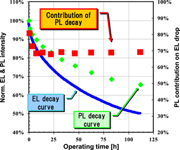
Figure 6. Degradation curves of EL and PL peak intensities of EL device containing a blue polymer during constant-current operation. Device structure: ITO/ HIL/ IL(20 nm)/ LEP(60 nm)/ cathode.
Download figure:
Standard image High-resolution imageIn the investigation of the PL decay mechanism, we have found that PL decay was not observed in the driving of mono-polar devices (hole-major or electron-major device) as shown in figure 7. These devices were fabricated with a similar procedure to the polymer OLED fabrication described above. The device structures of the hole-major and electron-major devices are ITO/HIL/IL/LEP/Au and Al/LEP/Alkali metal compound l/Al, respectively. We also performed degradation analysis of the host-guest polymer OLED device by reverse engineering techniques. The polymer OLED device was fabricated with a host polymer and guest emitter compounds. After degradation, the device was decomposed for chemical analysis of the host and guest materials, and the following results have been obtained:
- •no change in the photoluminescence efficiency of the guest emitter;
- •formation of an insoluble layer of polymer.
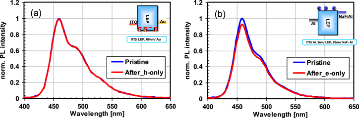
Figure 7. PL spectra of OLEDs before and after they were operated at 25 mA cm−2 for 130 h: (a) hole-driven device and (b) electron-driven device.
Download figure:
Standard image High-resolution imageThese observations indicate that (1) the PL decay of emissive materials is related to the excited state by the recombination of carriers, (2) PL decay does not originate from the degradation of the emissive unit, but from the creation of quenching sites in the host polymer.
Based on these findings, we designed more robust polymer materials by optimizing substituents to backbone and/or using more rigid units to reach double digit improvements of device lifetime.
2.4. Future trend of R&D in polymer OLED materials
2.4.1. Improvement of device performance
In practical applications, the further improvement of operating lifetime is a critical issue. Regarding the lifetime, sticking image lifetime (LT95) is important in addition to half-life time in luminance (LT50).
Self-emissive displays like OLEDs tend to get into a sticking image problem, which is the reduction of luminance in a specific area caused by continuous emission. To solve this issue, both material improvements to suppress the image sticking phenomenon and the development of operating methods are necessary. In the case of small molecule OLEDs, new materials showing LT95 of more than 500 h have been reported [44]. On the other hand, the development of polymer materials for a longer LT95 is still ongoing towards a practical level, however some investigations have been giving hints on how to solve this issue [41]. It was observed that removal of the triplet exciton from the backbone polymer could significantly improve the stability of the device, particularly at the early stage of driving, i.e. introducing a triplet quenching additive leads to the improvement of device lifetime (see figures 8 and 9). Careful adjustment is expected to satisfy both the need for high efficiency and a stable lifetime. Such comprehensive efforts, including material developments and detailed analysis, can bring polymer OLEDs to the goal of device performance required for practical usage.
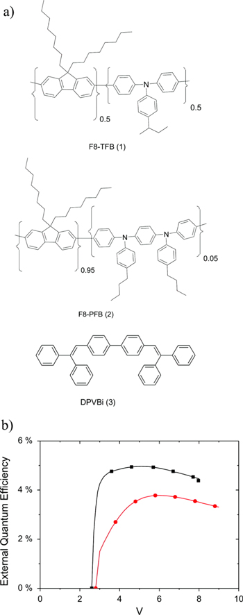
Figure 8. (a) Chemical structures of the materials under study. (b) External quantum efficiency of a prototypical PLED device comprising an F8-PFB LEP and a TFB interlayer, without (▪) and with (•) the addition of the triplet quenching additive (3). (Reprinted with permission from [41], ©2011 American Institute of Physics.)
Download figure:
Standard image High-resolution image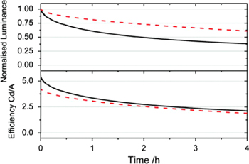
Figure 9. The decay of the device luminance (upper panel) with time and the change in efficiency of the device with time (lower panel) for a standard device (solid line) and a device containing the triplet quenching additive (dashed line). The devices were both driven from a starting luminance of 5000 cd m−2. (Reprinted with permission from [41], ©2011 American Institute of Physics.)
Download figure:
Standard image High-resolution imageAnother trend is low power consumption as a general environmental countermeasure. Hole injection materials and electrodes are newly developed for this purpose as well as emissive materials. These kinds of materials used in small molecule OLED devices are also being tested in polymer OLEDs.
2.4.2. Next direction of R&D for polymer emissive materials
As already mentioned, polymer emissive materials have the unique feature that various required functions can be introduced into a single polymer by designing functional units and co-polymerization techniques. This feature takes advantage of the applicability of printing processes for large area device fabrication or color patterning. In terms of the aforementioned points, many kinds of emissive polymers have been investigated [45]. For higher efficiency, phosphorescent materials with a combination of small molecular phosphorescent compounds and carrier transporting polymers have been proposed as polymer phosphorescent OLED materials. In that study, non-conjugated polymers with carrier transporting units attached to their side chains were commonly used. This type of polymer was considered to be easier for controlling singlet or triplet energy levels and other physical parameters. Basic research for understanding the effect of carrier transporting units on phosphorescent units using non-conjugated polymers other than PVCz has continued [46, 47]. The combination of polymers and phosphorescent emitters is very important to obtain high efficiency in further investigations. Recently new conjugated polymers which can be used as blue phosphorescent materials were reported [48]. They have polyphenylene chains connected by meta-linkage in the main chains, and exhibit 4.69 cd A−1 efficiency originating from a typical light-blue iridium complex, Firpic. As conjugated polymers with delocalized electrons, they possess excellent carrier transport properties, and the design policy of soft-controlled conjugation is studied for better and improved materials.
As another approach, research on the phase separation in polymer blends is ongoing to uncover clues about high efficiency. In some trials, adding polystyrene to conjugated polymers has shown an increase in efficiency [49], and the investigation of a relation between EL properties and phase separation in conjugated polymer mixtures was reported [50].
We would like to introduce new topical high efficiency materials. There have been two approaches of materials systems to obtain high efficiency; TTA fluorescent materials using an up-conversion mechanism, and phosphorescent materials utilizing emissive triplet levels. As an up-conversion mechanism other than TTA, a thermally activated delayed fluorescence (TADF) process was proposed for converting non-emissive triplet excited states into emissive singlet excited states [51]. The energetic development of TADF materials was started to give us other options to avoid potential issues such as the use of the rare metal iridium, difficulties in developing pure blue phosphorescent materials, and so on. As in the energy diagram shown in figure 10, the feature of TADF materials is considered as a small energy difference (ΔEST) between the singlet (S1) and the triplet (T1) energy levels [52, 53]. TADF materials, which thermally activate the reverse intersystem-crossing (ISC) from the triplet excited state to the singlet excited state, lead to an increase of fluorescence intensity, therefore high EL efficiency can be achieved in OLEDs with TADF materials. Furthermore, the roll-off characteristics of the EL efficiency can be reduced if the rate constant of the reverse ISC is significantly larger than the phosphorescent decay rate. Adachi's group started a search for efficient TADF materials from tin (IV) fluoride-porphyrin complexes. TADF materials with various colors were reported [53, 54], and remarkable materials of pure blue with 10% EQE [55], deep blue with 14.5% EQE [56] and very high EQE of 16.5% [57] were obtained. This material design is expected to be introduced into polymer OLED materials.
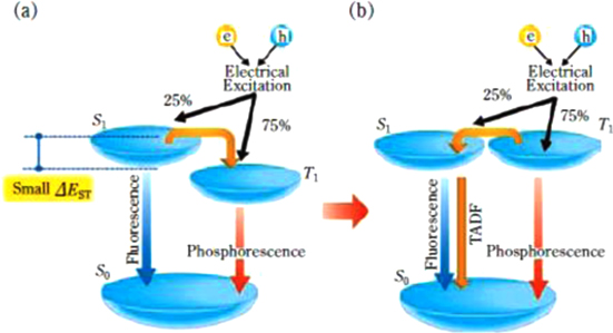
Figure 10. Process of formation of singlet and triplet excitons in the electroluminescence process (from figure 2 [53]).
Download figure:
Standard image High-resolution image2.4.3. Progress of soluble emissive materials
Small molecule OLEDs have a longer development history, so it takes a lead in practical usage compared with polymers. A vacuum evaporation method is used to form layers of OLED and many technical improvements have been developed in this area.
Recently, soluble small molecule materials have received much attention as many material companies have reported or press released their progress. Introducing soluble groups to existing emissive structures are common molecular designs [58]. As an OLED performance of soluble phosphorescent small molecules, LT50 of about 130 000 h in red, 150 000 h in green, and 8000 h in blue [59] have been observed, and are estimated to be close to evaporated type OLEDs.
Soluble small molecules are becoming competitive technologies versus polymers. It is considered that further progress in these soluble materials should accelerate the expansion and growth of the organic printed electronics market, including OLEDs.
3. Organic photovoltaic cell (OPV)
3.1. Features of OPV and its development history
It is well known that OPVs have features of thinness, light-weight and unbreakable flexibility. A high temperature fabrication process is not necessary for OPVs, and that makes it possible to use plastic films as substrates. OPVs also have flexibilities in the design of cells. Continuous manufacture using roll-to-roll process etc can reduce production costs, resulting in the creation of new application markets utilizing a variety of OPVs.
The R&D of OPVs was accelerated after Tang et al reported a 1% power conversion efficiency (PCE) by p-n heterojunction stacking type cell. Afterwards, Hiramoto [60, 61], Yoshino [62], and Heeger et al [63] independently proposed a bulk heterojunction (BHJ) type, which triggered further improvements in efficiency. In the case of BHJ cells, it is understood that the high PCE characteristics come from the efficient charge separations of photogenerated excitons at the inherent wide interface area of the p-n junction. Remarkable improvements in efficiency were achieved in around 2000 by using poly(3-hexyl thiophene) (P3HT) and [6,6]-phenyl-C61-Butyric Acid([C60]-PCBM) [64] for p-type and n-type semiconductors respectively. Along with this trend, an efficiency of 4 ∼ 5% was achieved in 2005 [65, 66]. In subsequent developments, newly proposed materials and tandem structures contributed to very rapid progress in efficiency, achieving higher PCEs of over 10%.
3.2. Improvement of OPV efficiency
3.2.1. Working mechanism of OPV and guiding principles for higher efficiency
The output characteristics of photovoltaic cells (PVs) are shown in figure 11. The maximum area of an inscribed square in the current-voltage curve is the maximum power generation of the PV. The maximum efficiency η is expressed as

where Jsc is the current density at a voltage of 0 V (short circuit current density), Voc is voltage at the current density of 0 mA cm−2 (open circuit voltage), and FF is the fill factor—the area of an inscribed square divided by (Jsc × Voc).

Figure 11. The current–voltage curve and the parameters of solar cell.
Download figure:
Standard image High-resolution imageGenerally the efficiency was measured by using a quasi-sunlight spectrum with 100 mW cm−2 as a light source.
The mechanism of the charge separation process is understood, as shown in figure 12. The process is considered to consist of the following four steps:
- (a)a photogenerated exciton is created in a photoelectric conversion layer;
- (b)the exciton moves to the interface of the p/n-junction;
- (c)the exciton separates into a hole and an electron when they reach the interface;
- (d)the hole and the electron are transferred to the cathode and anode respectively, and collected there.

Figure 12. Device structure of bulk hetero type and mechanism of charge separation.
Download figure:
Standard image High-resolution imageRecently, analytical techniques for the photogenerated charge separation process by femto-to-nanosecond laser have made an advance in exploring the detailed mechanism [67, 68] and the improvement of materials.
For higher conversion rates, increasing Jsc, Voc, and FF is necessary. As a guideline for increasing Jsc, absorbance, the rate of the photogenerated charge separation process, and suppression of the recombination of hole and electron can be listed.
Widening the range of absorption wavelengths is proposed, to increase absorbance. So far P3HT is a commonly used p-type semiconductor material. However P3HT absorbs wavelengths of up to about 650 nm so incident light with long wavelengths is not used effectively for power generation. Investigation of long wavelength absorbance polymers has been actively promoted. For this purpose, polymers were designed by placing electron donor and acceptor units alternately in a polymer chain. Such a configuration causes intra-molecule charge transfer to absorb longer wavelength irradiation. In figure 13, examples of newly developed polymers with long wavelength absorbance are shown. As table 3 shows, polymer 4 exhibited over 7% PCE in conjunction with appropriate electrode and buffer layers.

Figure 13. Examples of highly efficient p-type polymers.
Download figure:
Standard image High-resolution imageTable 3. Examples of OPV performances of long-wavelength absorption polymers.
| Polymer | Jsc (mA cm−2) | Voc (V) | FF | PCE (%) | Ref |
|---|---|---|---|---|---|
| 1 | 13.4 | 0.76 | 66.4 | 6.77 | [69] |
| 2 | 16.2 | 0.62 | 55 | 5.52 | [70] |
| 3 | 12.7 | 0.68 | 55 | 5.1 | [71] |
| 4 | 12.2 | 0.88 | 68 | 7.3 | [72] |
| 5 | 9.81 | 0.85 | 66 | 5.5 | [73] |
| 6 | 10.4 | 0.86 | 66.4 | 5.7 | [74] |
The control of photogenerated charge separation or the recombination of hole and electron is strongly related to phase separations as discussed in a later section.
Voc is related to the energy gap between the highest-occupied molecular orbital (HOMO) of a p-type semiconductor, and the lowest unoccupied molecular orbital (LUMO) of an n-type semiconductor. For the purpose of increasing Voc, the development of p-type semiconductor materials with a deep HOMO level and n-type semiconductor materials with a shallow LUMO level are required. The density-functional calculation is adopted extensively to pre-estimate these energy levels for molecular design.
It is considered that the FF is strongly correlated with the resistance of a PV cell. Utilizing high carrier mobility materials in the active layer, decreasing the resistance at the interface of each layer, and increasing the parallel resistance of PV equivalent circuits by removing defects in layers are all effective in increasing the FF value. OPV is expected to achieve high conversion efficiency by appropriate material designs.
3.2.2. Development of p-type polymers
We have explored p-type polymers for OPV materials based on our core technology of conjugated polymers. We developed fluorene polymers mainly in the early stage, and over a 6% PCE was obtained in conjunction with appropriate device process techniques.
Afterwards, we started to develop polymers with longer absorption wavelengths for the further improvement of efficiency. Our material design policy is shown in figure 14. In addition to the basic policy of band-gap reduction by strong interaction between electron donor units and electron acceptor units, planar donor units were introduced, giving an expansion of conjugation and high hole mobility, which are important for the carrier transfer after photogenerated charge separation. The molecular design and calculated absorption wavelength supported our efficient screening of units to obtain new polymers with very long absorption wavelength of over 900 nm.
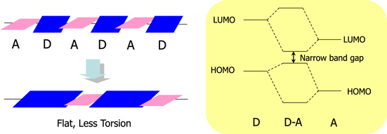
Figure 14. Concept of molecular design for narrow band gap polymers.
Download figure:
Standard image High-resolution imageBesides compressing the bandgap to obtain higher PCE, new materials with high FFs were also proposed [75]. At high internal electric fields or at near short-circuit conditions, enhanced bulk charge mobility can improve transport and reduce space charge build-up. However, at low internal fields or near Voc, long carrier lifetimes determine charge extraction and thus the steepness of the current-voltage curve. Accordingly, both carrier mobility and lifetime are target parameters to enhance, so as to increase the FFs. To optimize the FF, it was considered that highly ordered polymers with close π–π stacking could maximize mobility. Based on these considerations, the two units of thieno [3,4–c] pyrrole-4,6-dione (TPD) and 2,2'-bithiophene-3,3'-dicarboximide (BTI), shown in figure 15, were selected as effective building blocks for high mobility polymers. By introducing terthiophene (3T) with alkylation to promote ordering via side-chain interdigitation, it was assumed that combining BTI or TPD as the in-chain acceptor with 3T as the in-chain donor could imbue poly[5-(2-hexyldodecyl)-1,3-thieno [3,4–c] pyrrole-4,6-dione-alt-5,5-(2,5-bis (3-dodecylthiophen-2-yl)-thiophene)] (PTPD3T) and poly[N-(2-hexyldodecyl)-2,2'-bithiophene-3, 3'-dicarboximide-alt-5,5-(2,5-bis(3-decylthiophen-2-yl)-thiophene)] (PBTI3T). According to the evaluation of these polymers in the combination of [6,6]-phenyl-C71-butyricacid methyl ester (PC71BM) with an inverted bulk-hetero junction solar cell, they exhibited a high FF of ∼78% (see table 4).
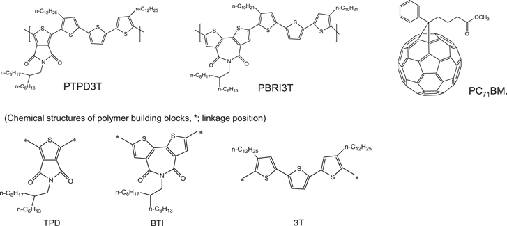
Figure 15. Chemical structures of polymer donors (PTPD3T, PBTI3T) and fullerene acceptor (PC71BM) [75].
Download figure:
Standard image High-resolution imageTable 4. Optimized photovoltaic response data for PTPD3T:PC71BM and PBTI3T:PC71BM inverted BHJ [75].
| Polymer | Voc (V) | Jcs (mAcm−2) | FF (%) | PCE (%) |
|---|---|---|---|---|
| PTPD3T | 0.786 | 12.3 | 78.7 | 7.72 |
| PBTI3T | 0.859 | 12.8 | 76.3 | 8.42 |
3.2.3. Controlling micro phase separation of active layer
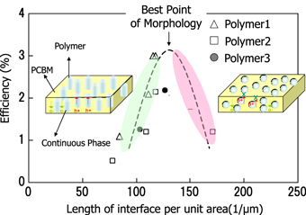
Increasing charge separation and charge transfer is useful for obtaining higher conversion efficiency. The average drift path of an exciton is about 10 nm so the micro phase separation size of p-type and n-type semiconductors should be controlled with a similar size of 10 nm.
For the investigation of controlling phase separation, quantification of the phase separation structure is needed. We observed the structure by processing transmission electron microscopy (TEM) images. We introduced a new parameter of interface length per unit area (unit; 1 μm−1) as an indicator to estimate the degree of phase separation, and to analyze the relation between conversion efficiency and phase separation.
As shown in figure 16, a clear correlation was observed, and an appropriate 'interface length per unit area' was determined.
Figure 16. Relation between morphology and efficiency.
Download figure:
Standard image High-resolution image
In the TEM tomography images showing microscopic phase-separated structures, an ideal formation of continuous domains in the direction of layer thickness was confirmed.
The phase separation structure was formed by an inkjet, or bar-coat, printing and drying process. It is known that such a structure size varies with solvents of inks [76, 77]. We took note of the solubility parameter (SP) value in selecting solvents and thus controlling phase separation size.
When a solvent with an SP value similar to that of fullerene derivatives, the size of the structure became smaller and the interface length became longer. This trend is understood, in that the p-type polymer is precipitated first to form fine networks, and afterwards the n-type fullerene derivative fills in the network to form small size phase separation structures. We achieved over 8% PCE by making use of this phase separation techniques.
3.2.4. Design and optimization of cell structures
As the impact of cell configuration on the efficiency is not small, the design and optimization of layer structures or thicknesses are critical factors in addition to the active materials or the control of phase separation. A thicker active layer gives a higher Jsc by increasing the absorbance of light. However this thicker layer results in decreasing charge collection by lowering the internal electric field. It also results in lowering the FF by increasing the resistance of the active layer. Furthermore, resistance at interfaces or external circuits has a harmful effect on efficiency. The optimization of cell structures should be tuned in consideration of these various factors.
A tandem device is one of the effective structures for obtaining high efficiency. Stacked active layers make it possible to absorb a wide wavelength range of incident light. In a tandem cell the active layers are connected in series, therefore Voc is higher than that in a single cell. On the other hand, Jsc becomes lower than in a single cell due to reduced absorbance in each stacking structure.
We optimized the layer thicknesses of such tandem cells, and the material selection of the interconnecting layer to obtain 10.6% PCE with Prof. Yang of UCLA [78].
3.3. Next direction of R&D for polymer OPV materials
Given that the OPV industry is well on its way to market entry, R&D in practical aspects will be more active. The investigation of high efficiency polymers has been widely examined so far [79–81], and will be continued. Not only the simple polymer design for higher performance but also the orientation of polymer chains or morphology will be focused on as research subjects. As mentioned in the previous section, the impact on device performance is strongly tied with morphology because the power generation process is affected by charge separation, carrier mobility, etc In succession to the previously reported studies [82, 83], further active research is expected.
We would like to point out that specifically designed polymers for OPV applications, (i.e. transparent polymers, specific colored polymers, etc) will be explored competitively to meet strong requests from industrial design. This is one of the next trends in OPV material developments.
From a standpoint of quality assurance of products, one of the most important issues is an understanding of degradation. OPV will not always be used in the same circumstances as Si type solar systems. A variety of durability test conditions and evaluation methods will be explored and established so OPV products can be evaluated appropriately. At the same time, degradation analysis will also be investigated in order to design new robust OPV materials.
The R&D of OPV modules and the fabrication process are also important in order to achieve practical products. A big gap in performance exists between large size modules and small size test cells. New materials should contribute to solving this problem by detailed gap analysis and adequate material design for large size panel fabrications.
4. Conclusions and perspective
In this article, the material technology in polymer OLEDs and OPVs was reviewed from their development histories to recent progress, including our experiences.
In the section on OLEDs, the features of OLEDs with polymers (PLEDs) were explained in comparison with OLEDs with small molecules. The main strengths of PLEDs are suitability to the printing process for device fabrication, and their simple device structure. Conjugated polymers can be well desinged to meet the required performances by co-polymerization technology. A variety of units have been developed, and polyfluorene is widely and practically used from standpoints of wide band gap and high conductivity of charge carriers.
Regarding polymer OLED performances, higher emission efficiency and longer operating device lifetime were picked up as the main subjects for development. We introduced an example of polymer design whereby controlling the hole mobility with amine unit contents in the polymer chain optimizes the emission efficiency. The impact of introducing an interlayer on the efficiency is an epoch-making technology in PLED, and TTA that is commonly used in fluorescent materials as a up-conversion technology was also introduced. By using these techniques, over 10% of EQE in a blue fluorescent PLED was obtained. Concerning device operating lifetimes, forming excited states was considered to be a key cause of the degradation process from the comparison of photoluminescence changes by operation of bipolar and monopolar devices.
In the last section on OLED, future trends of polymer OLED materials were indicated. Improvements of sticking image lifetime by the development of new materials is expected, and such investigation are predicted to become more active. Combinations of polymer and phosphorescent emitters, especially blue, was listed as one of these new materials. TADF, that is another up-coversion type material, was also introduced as a topical high efficiency material. As very high efficiency has already been obtained with small molecule type materials, it is expected that TADF will be applied to polymer materials as well.
In the OPV section, the main issue in the improvement of power PCE was explained, from the working mechanism of OPV, to guiding thoughts for higher efficiency. After the proposal of a BHJ type, remarkable improvements of PCE were obtained of over 4–5% with a combination of P3HT and [C60]-PCBM. A lot of p-type polymers were developed to improve the absorption wavelength range, Jsc, Voc, and FF. According to our material design policy, very long absorption wavelengths of over 900 nm were obtained. High FF materials were also designed by the concept of highly ordered polymers with close π–π stacking to enhance carrier mobility and lifetime. As a result, high FFs of around 78% were obtained. For higher PCE, the control of micro phase separation and the design of cell structures should also be considered in additon to materials development.
In the last part of the OPV section, the next direction of R&D for polymer OPV materials was discussed. In addition to continuous material development, R&D for the establishment and evaluation of durabilility tests, and further investigation and development of phase separation techniques will also be active.
For both of the technologies of polymer OLED and OPV, it can be said that fundamental material performances have become close to practical levels. However, we should understand that further efforts are needed to finish the material development to be used for electrical device products. Printed electronics materials are strongly tied to device architectures and fabrication processes to demonstrate their performances, thus parallel developments in materials and device/process are expected to be effectively promoted.
Acknowledgements
We acknowledge that a part of the OPV development reported here was supported by NEDO.