


Abstract
Pure and 1 at% gallium (Ga)-doped zinc oxide (ZnO) thin films have been prepared with a low-cost spin coating technique on quartz substrates and annealed at 500 °C in vacuum ∼10−3 mbar to create anion vacancies and generate charge carriers for photovoltaic application. Also, 0.5–1.5 at% extra zinc species were added in the precursor sol to investigate changes in film growth, morphology, optical absorption, electrical properties and photoluminescence. It is shown that 1 at% Ga–ZnO thin films with 0.5 at% extra zinc content after vacuum annealing for 60 min correspond to wurtzite-type hexagonal structure with (0001) preferred orientation, electrical resistivity of ∼9 × 10⁻³ Ω cm and optical transparency of ∼65–90% in the visible range. Evidence has been advanced for the presence of defect levels within bandgap such as zinc vacancy (VZn), zinc interstitial (Zni), oxygen vacancy (Vo) and oxygen interstitial (Oi). Further, variation in ZnO optical bandgap occurring with Ga doping and insertion of additional zinc species has been explained by invoking two competing phenomena, namely bandgap widening and renormalization, usually observed in semiconductors with increasing carrier concentration.
Export citation and abstract BibTeX RIS

Content from this work may be used under the terms of the Creative Commons Attribution-NonCommercial-ShareAlike 3.0 licence. Any further distribution of this work must maintain attribution to the author(s) and the title of the work, journal citation and DOI.
1. Introduction
Transparent conducting oxide (TCO) thin films exhibit high transparency (> 80% in the visible wavelength) and low electrical resistivity (< 10−2 Ω cm) simultaneously [1] and therefore are of immense interest for emissivity windows, gas sensors, flat panel displays, thin film transistors and light-emitting diodes [1–4]. Indium–tin oxide (ITO) is widely used as a TCO today due to its characteristics—resistivity (∼ 10−4 Ω cm) and optical transparency (∼ 80%). However, indium is toxic in nature, scarcely available and costly. This fact and the increasing demand for TCOs for large-scale application in the electronics industry requires development of alternative low-cost materials. Among various indium-free systems, zinc oxide (ZnO) has shown promise as it is cheaper, easier to etch and possesses high mechanical strength besides exhibiting high transparency in the visible range (energy bandgap Eg being 3.30 eV). However, its electrical resistivity is too high (∼ 103 Ω cm) to be used as a TCO [5]. So, group III elements such as aluminum (Al), boron (B), indium (In) and gallium (Ga) are used as dopant to make ZnO an n-type semiconductor and competitive TCO material. Further, doped ZnO thin films have been realized by a number of sophisticated techniques such as atomic layer deposition, sputtering, chemical vapor deposition and pulsed laser deposition on different substrates (glass, quartz, Si-wafer and sapphire) with optical transmittance of ∼70–95% and electrical resistivity of ∼10−1–10−4 Ω cm [6–9]. Sol-based spin coating has nowadays become attractive because of its simplicity, safety and low cost [10, 11].
The crystal defects usually present in ZnO include vacancies (Vo and VZn), interstitials (Oi and Zni), antisite occupancy (OZn and Zno) and impurities. Evidence for their existence is gathered from electron paramagnetic resonance, deep-level transient spectroscopy and photoluminescence (PL) [2, 12–14]. Among these techniques, PL is attractive as it renders direct correlation of optical properties with defect density. ZnO exhibits (i) ultraviolet (UV) emission by recombination of free excitons and (ii) deep-level broad visible bands due to defect centers. Thus, violet, blue, green, yellow, orange and red emissions observed in ZnO are associated with VZn, Vo, Oi, OZn, Zno and Zni, respectively [2–4, 13–20].
In this work, ZnO and 1 at% Ga–ZnO thin films have been prepared by a low-cost spin coating technique to investigate their characteristics for possible applications as TCOs. Ga is chosen as a dopant due to its poor reactivity and being oxidation resistant. The effects of Ga doping in spin coated ZnO thin films have been studied earlier also but by using 2-methoxyethanol as precursor solvent, mono-ethanolamine (MEA) as stabilizer and varying annealing conditions (namely temperature: 450–650 °C; time: 45–90 min; atmosphere: air alone or with forming gas (95% N2 + 5% H2) or (95.8% N2 + 4.2% H2)) in two steps [21–25]. Although the lowest electrical resistivity achieved falls in the range of 3.3 × 10⁻³–4.49 × 10⁻² Ω cm, it is reported without advancing any explanation [21, 22, 24]. In contrast, the uniqueness of the present paper lies in realizing spin coated conducting ZnO-based thin films for photovoltaic application by involving ethanol as solvent and combining three approaches, namely (i) low (∼ 1 at%) Ga doping to suppress secondary phases, (ii) vacuum annealing to induce oxygen deficiency and (iii) cation vacancy filling with additional zinc species using a chloride salt to avoid oxygen incorporation. The ethanol has the advantage over 2-methoxyethanol in terms of (i) evaporation, as boiling point is low (∼ 78 °C), (ii) lower carbon content, just 2 atoms per formula unit, (iii) better salt solubility, as dielectric constant is high (∼ 25) and (iv) lower toxicity [26]. Thin films have been characterized in terms of phase, morphology, optical absorption, electrical properties and PL.
2. Experimental details
Thin films of pure zinc oxide (ZnO) and 1 at% Ga-doped ZnO were prepared by a low-cost spin coating technique. For this, an appropriate amount of zinc acetate dihydrate (without or with gallium nitrate hydrate) was first dissolved in 45 ml ethanol and 5 ml of MEA added as stabilizer, stirred continuously at 80 °C for 1 h, and filtered. A few droplets of this solution (molarity 1 M) were then dropped over the spinning quartz substrate at 4000 rpm for 30 s with a glass syringe. A thin film so cast was dried subsequently at 400 °C for 10 min in air to remove the residue. The process was repeated 15 times to get a thin film of reasonable thickness and finally annealed in vacuum (∼ 10−3 mbar) at 500 °C for 15 or 60 min. The additional zinc species were introduced in the case of 1 at% Ga-doped ZnO by taking zinc chloride (an oxygen-free salt) suitably at the solution stage itself. The purpose was to fill zinc vacancies without additional oxygen. Note that ZnCl2 precursor has been used previously for preparing ZnO thin films with no evidence of chlorine ion contamination by spray pyrolysis in the temperature range of 300–500 °C [27–30]. The chlorine ion (Cl−) has low probability of getting accommodated at oxygen or interstitial sites because of being bigger in size (ionic radii of Cl− and O2− are 1.81 and 1.38 Å, respectively [31]). An x-ray diffractometer (X' Pert PRO) was used (with CuKα1 radiation, step size of 0.01° and time per step of 70 s) to identify phase(s), whereas an atomic force microscope (AFM, Molecular Imaging Pico-SPM) and field emission scanning electron microscope (FESEM, Carl Zeiss NTS GmbH-SUPRA 40VP) were employed for observing the film morphology. Further, optical absorption was measured in a UV–visible double-beam spectrophotometer (Hitachi Model U-3310) in the wavelength range of 300–900 nm with scan speed of 600 nm min−1. The electrical parameters such as sheet resistance (Rs), carrier concentration (n) and Hall mobility (μ) were obtained with the Van der Pauw configuration. In addition, the PL spectra were recorded with a spectrometer (Edinburgh steady-state fluorometer, FS 920 equipped with a Xenon flash lamp) in the wavelength range of 350–635 nm with a step of 1 nm and a slit width of 1 nm.
3. Results and discussion
3.1. Phase and surface morphologies
Figure 1 shows the x-ray diffraction (XRD) patterns of (i) ZnO and (ii) 1 at% Ga–ZnO (with 0–1.5 at% additional zinc species) thin films after annealing in vacuum ∼10−3 mbar at 500 °C for 15 or 60 min. All these patterns correspond to a wurtzite-type hexagonal structure similar to that of pure ZnO (a = 3.2495 Å, c = 5.2069 Å, Z = 2, space group = P63mc [32]) with slightly lower c-parameter but having the (0001) preferred orientation. The average crystallite size 'D' has been determined from the Scherrer's formula [33], D = 0.9λ/(B cos θ), where 'B' is the corrected full-width at half-maximum (FWHM) of diffraction peak, 'θ' is the Bragg angle and 'λ' is the wavelength of x-rays. The degree of orientation f(hkil) is estimated from [34]

with

and

where I(hkil) refers to the peak intensity of hkil reflection and ΣnI(hnkninln) is the sum of the intensities of all peaks in the ZnO films; Io(hkil) and ΣnIo(hnkninln) are the corresponding intensities of the standard polycrystalline sample. The values of lattice parameter (c), average crystallite size (D) and degree of orientation [f(0001)] determined from the 0002 diffraction peak data are summarized in table 1. Notice that the addition of Ga in ZnO leads to a decrease of both the c-parameter and the average crystallite size (D) with suppression of the degree of preferred orientation. The decrease in c-parameter is evident from the shift of 0002 diffraction peak toward a higher Bragg angle with the addition of Ga species in ZnO (inset of figures 1(a) and (b)). This happened possibly due to the replacement of Zn2+ species with relatively smaller Ga3+ ions (ionic radii being r(Zn2+) ∼ 0.60 Å, r(Ga3+) ∼ 0.47 Å for the coordination number of four) [31]. Moreover, the zoom versions of 0002 diffraction peak presented in the insets of figure 1 reveal the increase in its FWHM clearly. The introduction of additional zinc species in 1 at% Ga–ZnO thin films causes no perceptible change in c-parameter but leads to increase in crystallite size and improvement in the degree of preferred orientation (figure 2). When the annealing time is increased from 15 to 60 min, both the 'D' and the f(0001) increase further. The average size (D) seems to give the crystallite dimension along the c-parameter in which growth is occurring preferentially (as shown later with AFM images, figure 3).

Figure 1. X-ray diffraction patterns of ZnO and 1 at% Ga–ZnO thin films (with 0–1.5 at% extra zinc species), prepared by spin coating using sol of molarity 1 M on quartz substrate, after annealing at 500 °C in vacuum ∼10−3 mbar for (a) 15 min and (b) 60 min.
Download figure:
Standard image High-resolution image
Figure 2. Variation of degree of orientation [f(0001)] and crystallite size (D) of 1 at% Ga–ZnO thin films with (0–1.5 at%) extra zinc content after vacuum annealing for 15 and 60 min.
Download figure:
Standard image High-resolution image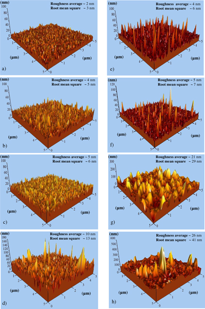
Figure 3. AFM images of 1 at% Ga–ZnO thin films (with 0–1.5 at% extra zinc species) after annealing at 500 °C in vacuum ∼10−3 mbar for (a)–(d) 15 min and (e)–(h) 60 min.
Download figure:
Standard image High-resolution imageTable 1. Lattice parameter (c), crystallite size (D), degree of orientation [f(0001)], Urbach width (ΔEu), ΔEBM, Ego + ΔEBM, Ego − ΔEBGN, resistivity (ρ), carrier concentration (n) and mobility (μ) values of ZnO and 1 at% Ga–ZnO thin films (with 0–1.5 at% extra zinc species).
| Annealing time (min) | 15 | 60 | ||||||||
|---|---|---|---|---|---|---|---|---|---|---|
| Thin films, annealed at 500 °C, vacuum (10−3 mbar) | ZnO | 1 at% Ga–ZnO+y at% additional zinc species | ZnO | 1 at% Ga–ZnO+y at% additional zinc species | ||||||
| 0 | 0.5 | 1.0 | 1.5 | 0 | 0.5 | 1.0 | 1.5 | |||
| Condition/parameter | ||||||||||
| c (Å)±0.002 | 5.201 | 5.193 | 5.193 | 5.193 | 5.190 | 5.201 | 5.194 | 5.191 | 5.191 | 5.191 |
| D (Å) ± 1 | 385 | 269 | 275 | 289 | 290 | 376 | 271 | 279 | 298 | 306 |
| f(0001) | 0.878 | 0.812 | 0.855 | 0.885 | 0.890 | 0.880 | 0.836 | 0.889 | 0.909 | 0.921 |
| ΔEu (meV) | 59 | 70 | 68 | 57 | 70 | 60 | 100 | 94 | 81 | 87 |
| Eg (eV) | 3.29 | 3.31 | 3.31 | 3.31 | 3.31 | 3.29 | 3.31 | 3.31 | 3.31 | 3.31 |
| ΔEBM (eV) | 0.035 | 0.039 | 0.046 | 0.089 | 0.055 | 0.086 | 0.088 | 0.095 | ||
| Ego+ΔEBM (eV) | – | 3.325 | 3.329 | 3.336 | 3.379 | – | 3.345 | 3.376 | 3.378 | 3.385 |
| Ego−ΔEBGN (eV) | – | 3.275 | 3.271 | 3.264 | 3.221 | – | 3.255 | 3.225 | 3.222 | 3.215 |
| ρ (Ω cm) | 1.46 | 0.024 | 0.016 | 0.031 | 0.029 | 1.19 | 0.017 | 0.009 | 0.017 | 0.034 |
| n (1018 cm−3) | – | 5.43 | 6.27 | 7.74 | 22.60 | – | 10.63 | 21.60 | 21.90 | 24.80 |
| μ (cm2 V−1 s−1) | – | 47.96 | 62.30 | 26.05 | 9.50 | – | 34.52 | 32.15 | 16.78 | 7.41 |
The values of surface energy (γ) of the exposed  ,
,  and (0001) planes of ZnO are 3.4, 2.0 and 1.6 J m−2, respectively [35]. Thus, basal plane (0001) has the minimum surface energy (γ) as well as the highest density of terminal/exposed zinc or oxygen ions [36, 37]. This makes growth of ZnO thin films thermodynamically favorable along [0001] direction [36, 38]. Several research groups have prepared pure and doped ZnO thin films by the solution method and found preferential growth along [0001] to depend on precursor, stabilizer, sol molarity, solution ageing, substrate, pre- and post-annealing temperature, and thickness [39–46]. Other reasons such as small crystallite size of the initial layer, strain minimization and compressive stress present are also cited for preferred growth along [0001] in ZnO system [44, 47–49]. The strain (εzz) was determined from [47, 50]

where c and co (5.2069 Å) are the lattice parameters of ZnO thin films and bulk, respectively [32]. Accordingly, 1 at% Ga-doped ZnO samples reveal compression along the c-direction with strain (εzz) of ∼0.26% in magnitude after annealing in vacuum at 500 °C against the value of 0.11% deduced under similar conditions for pure ZnO. The insertion of extra zinc species has practically no observable effect on strain. However, the degree of orientation is marginally higher in films subjected to prolonged treatment (60 min) in vacuum.
The precursor sol described as (Zn–O–CH2–CH2–NH2) upon casting a thin film and pre-heating at 400 °C for 10 min in air decomposes to ZnO [10]. The formation of oxide involves nucleation and growth processes. At the initial stage, nuclei formed on quartz substrate tend to orient along a preferred direction and are governed by interfacial energies. The equilibrium shape of nucleus is described by Young's equation [51, 52]

where γ represents the surface energy with subscripts q, f and qf standing for quartz substrate, film and quartz–film interface, respectively, and θ is the contact angle. The nucleus is a cap with circular base of radius (r sin θ), r being the radius of the sphere representing the cap. The surface energy of quartz (γq) is 0.3 J m−2 whereas γf for ZnO (0001) face is 1.6 J m−2 [53]. Since surface energies (γq, γf, γqf) are all positive and γq < γf, equation (3) yields 90° ⩽ θ ⩽ 144° for γq ⩽ γqf ⩽ γf. The nucleus partially wets the substrate and the first layer of deposition yields caps of various θ and/or size (i.e. radius of representing sphere). For subsequent layers, γ is nearly equal to γf for the exposed surface and γff ∼ 0 for the new interface (ff). Hence equation (3) corresponds to a small contact angle (few degrees) for the upper cap which is set to wet the surface. The alignment of (0001) face improves with heating at each step and remains confined at the flat portion of the curved cap. Consequently, growth occurs preferentially along the [0001] direction vertically with reduction of base area progressively, forming crystallites of conical morphology.
The results suggest that Ga doping in ZnO induces formation of small crystallites with decrease in c-parameter and suppresses the degree of orientation as well. On the other hand, insertion of extra zinc species somehow increases the average crystallite size without noticeable change in c-parameter but with some improvement in the degree of preferred orientation (figures 1(a) and (b)). In fact, while a few zinc ions assume cation vacant positions, others occupy interstitial sites. The former process relaxes the strain depending on the nature of vacancy (VZn0,VZn1−, VZn2−) [54] and releases electrons to improve the electrical conductivity (section 3.3), the latter causes strain so as to maintain the effect of Ga doping unaltered.
Figures 3(a)–(h) show three-dimensional AFM images of 1 at% Ga–ZnO (with 0–1.5 at% additional zinc species) thin films taken within the scan range 5 μm × 5 μm. These images were analyzed by a scan probe image processing software (SPIP 6.0.3) for surface morphology parameters, namely (i) root-mean-square roughness (Rrms), (ii) average roughness (Rav) and (iii) height of growth structure. The results indicate increase in film roughness with both vacuum annealing and addition of extra zinc species; the highest values of Rrms and Rav being ∼41 and ∼26 nm, respectively, for 1 at% Ga–ZnO thin films (containing 1.5 at% of additional zinc species) after vacuum annealing at 500 °C for 60 min (figure 3h). The increase in surface roughness is caused by addition of extra zinc species due to improvement in the degree of preferred orientation (0001) and average crystallite size [55–57] as shown clearly in figure 2. The growth process yields conical grain morphology with height (lying perpendicular to the substrate and in the range ∼13–114 nm) determined by annealing time, additional zinc species and the degree of orientation [f(0001)].
3.2. Optical behavior
Figures 4(a) and (b) show the optical transmittance spectra of thin films of ZnO and 1 at% Ga–ZnO (with 0–1.5 at% additional zinc species) after annealing in vacuum ∼10−3 mbar at 500 °C for 15 or 60 min. These spectra display ∼60–100% transmittance in the wavelength range of 400–900 nm with some interference fringes useful for determination of film thickness (t) by the envelope method [58]. The thickness (t) is given by

with

and

where nλ1 and nλ2 are the refractive indices of thin film at the two adjacent maxima (or minima) for λ1 and λ2, ns is the refractive index of the substrate, Tmax and Tmin are the transmittance values of the upper and lower envelopes, respectively, for a given wavelength (i.e. λ1 or λ2). Thus, the thickness of thin films prepared with 15 coatings comes out to be ∼694 ± 58 nm. Note that the thickness (t = 625 nm) measured by FESEM cross-sectional image (figure 5) of 1 at% Ga–ZnO with 0.5 at% additional zinc species, matches well with the value determined above by the envelope method.
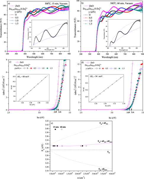
Figure 4. Optical transmittance spectra of ZnO and 1 at% Ga–ZnO thin films (with 0–1.5 at% extra zinc species) after annealing at 500 °C in vacuum ∼10−3 mbar for (a) 15 min and (b) 60 min with insets depicting interference fringes and envelopes above 400 nm, (c) and (d) (αhυ)2 versus hυ plot and ln(α) versus hυ plots (inset) of films after vacuum annealing for 15 and 60 min, respectively. (e) Variation of energy bandgap with carrier concentration.
Download figure:
Standard image High-resolution image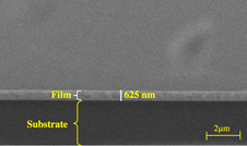
Figure 5. Cross-sectional FESEM image of a 1 at% Ga–ZnO thin film with 0.5 at% additional zinc species, after vacuum annealing at 500 °C for 60 min.
Download figure:
Standard image High-resolution imageZnO has a direct bandgap with oxygen (3P2) as valence band and Zn2+ (1So) as conduction band [59]. Its optical bandgap (Eg) and defect-induced band tailing parameter (ΔEu = {d[ln(α)]/d[hυ]}−1) have been obtained from (αhυ)2 versus hυ or Tauc plot and ln(α) versus hυ plot [10, 60], respectively (figures 4(c) and (d); table 1). While ZnO thin films after annealing for a short duration (i.e. 15 min) display high optical transmittance of ∼90% due to low surface roughness [10], those subjected to prolonged treatment of 60 min exhibit poor transmittance, high surface roughness and a large Urbach width (ΔEu) of ∼94 meV (notice increased bandgap tailing in figure 4(d)). The decrease in transmittance can be attributed to additional scattering resulting from the increased surface roughness of films. The addition of 1 at% Ga in ZnO leads to (i) increase/decrease in transmittance in the wavelength range of 400–700 nm when the film is annealed in vacuum for short/prolonged (15/60 min) duration in vacuum, (ii) increase in the optical bandgap or a blue shift and (iii) increase of Urbach width due to impending rise in defects (table 1).
The addition of extra zinc species in 1 at% Ga–ZnO thin films causes (i) almost no change in the optical bandgap even though the carrier concentration is rising and (ii) decrease and then increase in the Urbach width (table 1). Incidentally, the values of Urbach width (ΔEu) deduced above are much smaller than the 84–467 and 86–659 meV found in Ga–ZnO samples prepared by e-beam deposition [61, 62]. These facts indicate the presence of low defect density and less strain in thin films produced by the sol-based spin coating method.
The increase in the optical bandgap occurs with a rise in the carrier concentration and is explained in terms of the Burstein–Moss (BM) effect. The increase in bandgap is given by [63–67]

Thus, ΔEBM can be evaluated for different 'n' provided the effective mass of electron (me*) is known. Taking me* = 0.38mo (5.099 × 10⁵ eV/c2) [67–70] and carrier concentration as obtained from the Hall measurements (section 3.3), ΔEBM values determined from equation (5) are given in table 1.
The bandgap versus 'n' plot shown in figure 4(e) indicates the estimated value of (Ego + ΔEBM) to be much larger than the measured data. It means another phenomenon involving reduction in bandgap is operational as well above a critical carrier concentration of 3.51 × 1018 cm−3 (figure 4(e)) or Mott density (nMott) by merging of donor levels with the conduction band. Mott density is given by nMott = (0.2 me* π e2 /h2 ε )3, where me* is effective mass of electron, and ε = εr εo stands for the dielectric constant [71]. Taking me* = 0.38mo and ε = 8.65εo (εo = 8.85 × 10⁻¹² F m−1), nMott turns out to be 4.61 × 1018 cm−3. When the carrier density increases, an important parameter (rs) (defined as the ratio of half inter-electron separation and Bohr radius ratio) determines the degeneracy and, in turn, electron–electron correlation—giving rise to downward shift of the conduction band as well [71–76]. The ratio rs is given by [77]

where mr is the carrier effective mass ratio (m*/mo), εr is the relative permittivity of the semiconductor and n is the carrier concentration. When the ratio rs is less than unity, bandgap narrowing occurs. In the limit rs = 1, the carrier concentration (n = nB) can be evaluated from equation (6) with εr = 8.65, mr = 0.38 for ZnO [47, 54] as 1.7 × 1019 cm−3. This essentially means that bandgap narrowing in ZnO should be observed at carrier concentration higher than 1.7 × 1019 cm−3. Incidentally, this value is comparable to or larger than the measured carrier density at which bandgap narrowing seems to be occurring in ZnO. Obviously, the electron–electron interaction condition is relaxed somewhat, i.e. it is applicable even if rs is slightly more than unity. The bandgap narrowing (ΔEBGN) values can be deduced from the expression

where Ego ∼ 3.29 eV is the optical bandgap of pure ZnO sample, Eg is the bandgap derived from the optical absorption data and ΔEBM is found from equation (5). The results can be accounted for by considering variation of ΔEBGN data with carrier concentration. ΔEBGN versus n1/3 plot in fact gives a straight line whose intercept at n1/3-axis gives the carrier concentration for zero bandgap narrowing as 3.72 × 1018 cm−3. The straight line can be represented as

with A representing the slope. Thus, (Eg–ΔEBGN) and Eg follow the trends with carrier concentration as shown in figure 4(e). Note that the experimental values of Eg lie on the curve itself.
3.3. Electrical properties
Figure 6(a) shows the disposition of zinc and oxygen ions in the wurtzite-type hexagonal structure of ZnO. The bond lengths along the c-direction and off c-axis are given by L = cu, and L1 = √[(a2/3 + (0.5 − u)2c2], respectively, with u = a2/3c2 + 1/4; a and c being the hexagonal unit cell parameters. Similarly, the bond angles α and β (figure 6(a)) are expressed as [78]


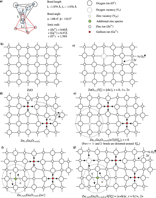
Figure 6. Schematic diagrams showing (a) tetrahedral coordination and (b)–(g) 2D representation of ZnO: (b) pure, (c) vacuum annealed, (d) Ga doped with oxygen absorption, (e) Ga doped with creation of zinc vacancies, (f) and (g) cation vacancies filled with extra zinc species without and with vacuum annealing, respectively.
Download figure:
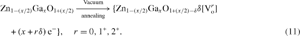
Standard image High-resolution imageThe electrical conductivity of ZnO may be enhanced by (i) creation of oxygen ion vacancies and (ii) substitution of Zn2+ species with higher valence metal (namely Ga, Al, In or Zr) ions. The creation of an oxygen–ion vacancy allows the associated two electrons to become free and/or form F-centers. The system may then be represented by (ZnO1−δ δ [Vor ] + [rδ e−]), where Vor is oxygen vacancy with charge r = 0, 1+ or 2+ (figure 6(c)). Consequently, local tensile strain can develop around the oxygen vacancy if r = 0 or 1+. The electrical conductivity (σ) of ZnO may therefore increase with the available number of free electrons. A metal (say Ga) ion may substitute the Zn2+ site in two possible ways:
- (a)Each Ga3+ ion replaces a Zn2+ ion and donates an electron to combine with an extra oxygen available to give the composition Zn1−xGaxO1+(x/2) of an insulator (figure 6(d)). Also, local compressive strain is developed around the Ga ion due to its 3 + charge. If oxygen deficiency is already present, electrons released by Ga3+ ions contribute to conductivity (as described above for pure ZnO).
- (b)Two Ga3+ ions replace two of the three Zn2+ ions and create one cation vacancy (ensuring charge neutrality) leading to the composition Zn1−(3x/2)GaxO(x/2)[VZn] (VZn stands for the zinc vacancy) provided zinc content in the precursor is suitably (i.e. x/2) reduced. The electrons donated by Ga3+ ions may fully or partially compensate for zinc vacancy by giving off no carrier or creating electron–hole pairs. Alternatively, the composition is written as Zn1−xGaxO1+(x/2)(x/2)[VZn] if zinc content is not reduced (figure 6(e)). In this situation, all the three possibilities, namely no charge carrier, e–h pairs and free electrons are expected to prevail simultaneously.
The filling of cation vacancies by additional zinc species (without oxygen uptake) can provide extra electrons to improve the conductivity with the composition becoming Zn1−xGaxO[xe−] or Zn1−(x/2)GaxO1+(x/2)[xe−] (figure 6(f)). These processes can be described by


Such a treatment is likely to increase the conductivity (σ) of a ZnO-based system.
The sheet resistance (Rs) and carrier concentration (n) are obtained by current–voltage characteristics and Hall effect measurements, respectively, in Van der Pauw configuration. The electron mobility (μ) is deduced from

where 'ρ' is the resistivity, 'e' is the electronic charge and 't' is the thickness of the film. Table 1 summarizes the electrical parameters of ZnO and 1 at% Ga–ZnO without and with extra zinc species. Note that the values of electrical resistivity of pure ZnO thin films after annealing in vacuum ∼10−3 mbar at 500 °C for 15 and 60 min are ∼1.46 and 1.19 Ω cm, respectively. It may be mentioned that the resistivity of as-prepared ZnO thin films (thickness ∼625 nm) is 41 Ω cm. This value is comparable to the reported value of ∼56 Ω cm for 300 nm thick films prepared with 0.5 M precursor solution in 2-methoxyethanol [24]. However, the resistivity enhances from 41 to 900 Ω cm upon annealing the films in air at 500 °C for 1 h [10]. The low resistivity of ∼1.19 Ω cm is obtained here with release of electrons accompanying oxygen desorption (i.e. creation of anion vacancies) via annealing of ZnO thin films at 500 °C for 60 min in vacuum ∼10−3 mbar.
With addition of 1 at% of Ga, the resistivity values decrease substantially from 1.46 to 0.024 Ω cm and from 1.19 to 0.017 Ω cm (table 1). Further reduction in resistivity occurs with the introduction of 0.5 at% extra zinc species and the values become 0.016 and 0.009 Ω cm, respectively. However, 'ρ' begins to increase with additional zinc content beyond 0.5 at%. Thus, 1 at% Ga–ZnO thin films with 0.5 at% extra zinc species after annealing in vacuum at 500 °C for 60 min depict lowest sheet resistance of ∼139 Ω/□ (resistivity ∼0.009 Ω cm).
Hall effect measurements suggest 1 at% Ga–ZnO thin films to be n-type and reveal progressive increase in carrier concentration with rising extra zinc content. The increase is even greater when annealing time is enhanced from 15 to 60 min; the carrier concentration reaches a figure of 2.16 × 1019 cm−3 for 1 at% Ga–ZnO (with 0.5 at% extra zinc species) after vacuum annealing at 500 °C for 60 min. The electron mobility value decreases continuously with increase of extra zinc species. The exception has been with 0.5 at% Zn containing Ga–ZnO thin films annealed for shorter duration (15 min) where 'μ' is high (∼ 62.3 cm2 V−1 s−1). There is no plausible explanation available as yet for this observation. Since the resistivity (ρ) is essentially determined by the product of 'n' and 'μ', any change in ρ can result due to variation of either or both. The resistivity depends on the microstructure of films too and varies from sample to sample. Repeated experiments have shown that while the carrier concentration remains of the same order, ρ varies markedly in films causing uneven changes in 'μ'. The values of 'μ' obtained here are however comparable to or larger than those reported for Ga–ZnO thin films prepared by other methods, namely (i) r.f. sputtering, 6–10 cm2 V−1 s−1 [79], (ii) spray pyrolysis as such and after annealing in air and oxygen; 18.99, 18.94 and 22.15 cm2 V−1 s−1 [80] and (iii) chemical spray, 0.1–2 cm2 V−1 s−1 [81].
Electrical resistivity is determined by the product of carrier concentration (n) and mobility (μ), leading to a lower value when (nμ) is large. The carrier concentration of ZnO increases by (i) Ga doping, (ii) filling of cation vacancies with extra zinc species as described by reactions (10a) and (10b), and (iii) oxygen desorption following vacuum annealing as per reaction (11). Also, mobility (μ) decreases with increase in carrier density due to scattering from grain boundaries, intragrains and ionized impurities [68, 82].
3.4. Photoluminescence
PL measurements provide useful information about the nature and energy level of defects present. PL spectra of thin films of 1 at% Ga–ZnO with 0–1.5 at% additional zinc species after annealing in vacuum ∼10−3 mbar at 500 °C for 15 or 60 min with the excitation wavelength of 325 nm are shown in figures 7(a)–(f) in three different wavelength ranges of 360–460, 450–510 and 510–635 nm. In order to discuss the results in detail, the spectra of 1 at% Ga–ZnO and 0.5 at% additional zinc containing thin films are presented separately with Gaussian fitting of peaks (dotted curve; goodness-of-fit R2 ∼ 0.98–0.99) undertaken using an Origin software version 7.5 in wavelength range of 360–460 and 465–485 nm in figures 8 and 9, respectively. In the first regime (figure 7(a)), three PL peaks observed are at ∼380 nm (3.26 eV), ∼411 nm (3.02 eV) and ∼450 nm (2.76 eV) for 1 at% Ga–ZnO thin films annealed at 500 °C for 15 min. The UV emission at ∼380 nm (3.26 eV) arises due to near-band edge, i.e. 1So(Zn2+) → 3P2(O2−) transition involving recombination of excitons and corresponds to the optical bandgap of the material [13–20]. The emission peaks become somewhat broad and appear improved at 409 and 449 nm (height nearly equal to peak at 381 nm, figure 8(b)) on prolonged annealing (60 min) due to enhancement of defects and impending effects of non-radiative transitions. With addition of 0.5 at% zinc species, UV emission peak at ∼380 nm (3.26 eV) remains strong in comparison to other peaks (figure 8(c)) irrespective of short or prolonged vacuum annealing. This essentially means (i) reduction of defect levels near the band edge, (ii) suppression of non-radiative recombination processes and/or (iii) improvement in crystallinity of thin films. But, the violent emission at ∼411 nm (3.02 eV) is shifted to 394 nm (3.15 eV) or 389 nm (3.19 eV) with no perceptible shift peak at ∼450 nm. Both these peaks are, however, appearing suppressed with respect to UV emission at 380 nm.

Figure 7. PL spectra of 1 at% Ga–ZnO thin films (with 0–1.5 at% additional zinc species) after vacuum annealing at 500 °C for (a)–(c) 15 min and (d)–(f) 60 min.
Download figure:
Standard image High-resolution image
Figure 8. PL spectra together with Gaussian fitting of peaks (dotted lines) in the wavelength range of 360–460 nm for (a), (b) 1 at% Ga–ZnO as such and (c), (d) with 0.5 at% additional zinc species after vacuum annealing at 500 °C for (a), (c) 15 min and (b), (d) 60 min.
Download figure:
Standard image High-resolution image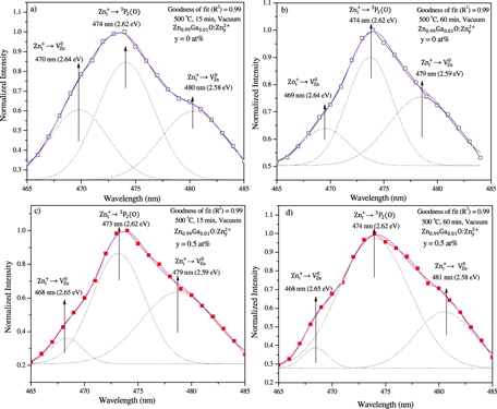
Figure 9. PL spectra together with Gaussian fitting of peaks (dotted lines) in the wavelength range of 465–485 nm for (a), (b) 1 at% Ga–ZnO as such and (c), (d) with 0.5 at% additional zinc species after vacuum annealing at 500 °C for (a), (c) 15 min and (b), (d) 60 min.
Download figure:
Standard image High-resolution imageSince the formation energy of zinc vacancies in ZnO is low [3, 54, 83], deep-level emissions at ∼411 nm (3.02 eV) and ∼450 nm (2.76 eV) may be attributed to them. Zinc vacancies are created by (i) replacing two cations by Ga3+ ions and forming (2GaZn–VZn) and/or (2GaZn–VZn–Zni) groups and (ii) annealing in vacuum creating (Vo–Zni) pairs. The origin of zinc vacancies has been discussed in detail in section 3.3 while dealing with the electrical conductivity of 1 at% Ga–ZnO thin films.
The second part (figure 9(a)) of the PL spectrum in the wavelength range of 465–485 nm of 1 at% Ga–ZnO thin films contains a peak centered around 474 nm (2.62 eV) with two shoulders at 470 nm (2.64 eV) and 480 nm (2.58 eV). After prolonged annealing (60 min), these peaks remain in nearly the same positions but their relative intensities change (figure 9(b)). With the addition of 0.5 at% zinc species, PL emission peaks make no or minor shifts with readjustment of relative intensities. In fact, zinc species fill cation vacancies and/or occupy interstitial positions (octahedral rather than tetrahedral) in the hexagonal structure because of geometrical constraints [3].
The third part (figures 7(c) and (f)) of the PL spectra covers the wavelength range of 510–635 nm and exhibits three peaks at ∼535 nm (2.32 eV), 576 nm (2.15 eV) and ∼624 nm (1.99 eV) for 1 at% Ga–ZnO thin films after annealing in vacuum for 15 min. With addition of 0.5 at% extra zinc species, the emission peak at 576 nm (2.15 eV) gets fully suppressed while the other two are diminished only partially.
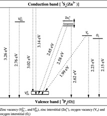
The native defects present in ZnO include (i) divalent zinc vacancy (VZn2−) and monovalent interstitial zinc (Zni+) as donors and located (0.4–0.7) eV below the conduction band [19, 84, 85], (ii) monovalent zinc vacancy (VZn1−) as an acceptor with energy level (0.3–0.7) eV above the valance band [19, 84, 85], (iii) monovalent oxygen vacancy (Vo1+) as a deep acceptor at (1.2–1.5) eV above the valence band [19, 84] and (iv) neutral impurities such as interstitial zinc (Zni0) and oxygen vacancy (Vo0) as shallow donors at 0.05 eV below the conduction band and neutral zinc vacancy (VZn0) as a deep accepter at 0.3 eV above the valance band [19, 84–86]. A list of defects and associated transitions in ZnO is given in table 2. Based on the present results and earlier reports, a schematic diagram of energy levels with respective transitions in ZnO is presented in figure 10.
Figure 10. Optical transitions involving energy levels of various defects in ZnO.
Download figure:
Standard image High-resolution image
Table 2. Summary of defect energy levels: zinc vacancy (VZn), zinc interstitial (Zni), oxygen vacancy (Vo) and oxygen interstitial (Oi) within ZnO bandgap.
| Deep-level emissions | |||||||
|---|---|---|---|---|---|---|---|
| Violet (nm) | Violet–blue (nm) | Blue (nm) | Blue–green (nm) | Green (nm) | Yellow (nm) | Orange (nm) | Orange–red (nm) |
| 411 (Vo) [87] | 434 (VZn) [87] | 466 (VZn) [87] | 490 (Zni→VZn) [17] | 496 (Vo) [15] | 582 (Oi) [17] | 620 (Oi) [15] | 625 (Vo→VZn) [94] |
| 400 (VZn) [15] | 435(Cu) [90] | 470 (Zni→VZn) [20] | 486 (Vo) [16] | 536 (Vo) [17] | 580 (Vo∼F2+) [18] | 617 ( ) [93] ) [93] |
|
| 413 (VZn) [88] | 470 (K) [20] | 484 (Zn+i →V−Zn) [93] | 525 ([Vo∼F+) [18] | 577 (Li) [16] | |||
| 424 (Zni) [88] | 459 (Zni→VZn) [91] | 521 (OZn) [19] | |||||
| 414 (Zni) [89] | 466 [92] | 523 (VZn) [16] | |||||
| 420 (VZn) [89] | 526 [92] | ||||||
| 410 (VZn) [90] | 518 (OZn) [93] | ||||||
| 438 (Zni) [90] | |||||||
| 411 (VZn)a | 450 (VZn)a | 480 (Zni→VZn)a | 535 (Vo)a | 576 (Oi)a | 624(Vo→VZn)a | ||
| 470 (Zni→VZn)a | |||||||
| 474 (Zni)a | |||||||
Ga doping in ZnO seems to produce zinc vacancies and donate free electrons as well. The presence of zinc vacancies is evident from two emissions at ∼411 nm (3.02 eV) and 450 nm (2.76 eV) and the nature of Urbach width (giving the signature of defects) observed in PL and optical absorption spectra, respectively (see, e.g. figures 8(a), (b) and 4(c), (d)). Notice that upon insertion of 0.5 at% extra zinc species, cation vacancies are filled and cause peak suppression with shift from 411 to 394 nm or no shift (at ∼450 nm) with simultaneous decrease of defects, i.e. Urbach width narrowing (table 1). Obviously, there are different types of zinc vacancies (VZn2−, VZn0), each forming a defect level (in some energy interval) within the bandgap. Zinc species occupy the cation vacancies (VZn0) of lower energy levels. Hence, the PL peak shrinks in both the cases but shifts toward lower wavelength for VZn0 (figure 8(a)–(d)).
4. Conclusions
Suitable Ga-doped ZnO thin films (having 0.5 at% extra zinc species) can be successfully prepared by a low-cost spin coating technique and subsequent annealing in vacuum for 60 min for photovoltaic application. The films exhibit wurtzite-type hexagonal structure similar to ZnO with preferred orientation (0001), optical transmittance of 65–90% in the visible range, electrical resistivity of ∼9 × 10⁻³ Ω cm and carrier mobility of ∼32.15 cm2 V−1 s−1. The improvement in (0001) preferred orientation is linked to processes responsible for increase in the average crystallite size, namely annealing time and insertion of extra zinc species. Moreover, films contain various defects, namely vacancies (zinc VZn and oxygen Vo) and interstitials (zinc Zni and oxygen Oi) and display 1So  ,
,  (O) and
  (O) main transitions at 3.02, 2.76 and 2.62 eV, respectively together with
  emission at 2.65 and 2.58 eV. The variation of optical bandgap (Eg) with increase in carrier density can be explained by two competing phenomena (namely bandgap widening and renormalization) operating simultaneously.