


Abstract
Bismuth (Bi) has attracted a great deal of attention for its strongest spin–orbit coupling (SOC) strength among main group elements. Although quantum anomalous Hall (QAH) state is predicted in half-hydrogenated Bi honeycomb monolayers Bi2H, the experimental results are still missing. Halogen atoms (X = F, Cl and Br) were also frequently used as modifications, but Bi2X films show a frustrating metallic character that masks the QAH effects. Here, first-principle calculations are performed to predict the full-cyanided bismuthene (Bi2(CN)2) as 2D topological insulator supporting quantum spin Hall state with a record large gap up to 1.10 eV, and more importantly, half-cyanogen saturated bismuthene (Bi2(CN)) as a Chern insulator supporting a valley-polarized QAH state, with a Curie temperature to be 164 K, as well as a large gap reaching 0.348 eV which could be further tuned by bi-axial strain and SOC strength. Our findings provide an appropriate and flexible material family candidate for spintronic and valleytronic devices.
Export citation and abstract BibTeX RIS

Original content from this work may be used under the terms of the Creative Commons Attribution 3.0 licence. Any further distribution of this work must maintain attribution to the author(s) and the title of the work, journal citation and DOI.
1. Introduction
Studies of two-dimensional (2D) materials with non-trivially topological properties are of great scientific and technical interests for their amazing and potential applications in spintronics and quantum computations. The research on topological electronic states started following the discovery of the quantum Hall (QH) effect in 1980, in which the novel concept of topological number was introduced to identify the novel quantum states beyond symmetry. However, a strong external magnetic field is required to realize the QH effect, therefore two novel quantum states dispensing with external magnetizations, the quantum anomalous Hall (QAH) effect and quantum spin Hall (QSH) effect, have now attracted a growing interest. The QAH effect is the quantum version of the traditional anomalous Hall effect, which was first predicted by Haldane [1] in 1988, and was experimentally confirmed in recent years [2]. The QSH insulator is the 2D version of a famous class of a novel material called a topological insulator (TI) [3–5]. It has a finite bulk band gap mainly caused by the spin–orbit coupling (SOC), and gapless edge channels protected by time-reversal symmetry from backscattering. In 2D materials, graphene is first identified to be TI [6], but with a frustrating small bulk gap as small as 10−3 eV. Subsequently, the research on 2D TI with large gap became intensive. Many efforts have been made to find appropriate candidate compounds of large-gap 2D TI, such as Ge [7], Sn [8–10], Sb [11], and Bi [12]. Among them, bismuth has the strongest SOC strength along main group elements, and the Bi (111) bilayer, named bismuthene, is found to be a candidate 2D topological insulator supporting QSH effects, and has attracted a great deal of attention.
The chemical functionalization is considered to be an effective way to alter the electronic properties of 2D materials with desirable features and a powerful tool to find new materials with diverse possibilities, for the wide and various options in hundreds of chemical groups [13–18]. Taking bismuthene as an example [19], pure bismuthene has a bulk band gap of about 560 meV, while halogen decorated bismuthene, which remains topological nontrivial, could reach a gap of up to 1 eV. Organic groups are alternative options to build novel 2D TI materials functional group, for their abundant chemical characters. Motivated by previous achievements, we reported [20] the QSH effect in ethynyl functionalized stanene with a bulk of 220 meV, and 203 meV in stanene cyanide [21]. Compared with QSH insulators (and TI), the studies on QAH effects are relatively few. Yan's group [22] proposed that the half-passivated stanene and germanene are QAH systems with a large energy gap. Remarkably, Lin [23] and Niu [24] et al reported that half-hydrogenated bismuthene (Bi2H) is a Chern insulator with giant gap. Unfavourably, the half-halogenated bismuthene Bi2X (X = F, Cl, Br and I) were found frustrating metallic characters. As is known, cyano group(-CN) has a similar chemical property to halogeno groups, hence cyanogen decorated bismuthene, if topological nontrivial, could be a diversified selection in spintronic devices. In this paper, we predict, by first-principles calculations, the cyanided bimuthene Bi2(CN)2 as a 2D TI supporting QSH state with a gap up to 1.10 eV. Notably, the half-cyanided bismuthene Bi2CN is predicted as a novel valley-polarized QAH insulator with band gap of 0.348 eV, in comparison to the metallic states in Bi2X family. Furthermore, the observed QAH effects of Bi2CN are tunable under bi-axial strains and SOC strength, both of which are applicable to realization in different substrates such as BN, MoS2, etc. We hope the organic molecule functionalizations on 2D films could provide new platforms for the designing of new quantum Hall state insulators.
2. Computational details
First-principle calculations are performed using plane wave basis Vienna ab initio simulation package (VASP) [25–28]. The projector-augmented wave (PAW) [29, 30] method is used to describe the electron-ion potential. The Perdew--Burke--Ernzerhof (PBE) [31] form exchange-correlation (XC) potential approximate is employed with a 500eV kinetic energy cutoff. The calculations using hybrid XC functional according to Heyd, Scuseria and Ernzerhof (HSE) [32] are also employed to verify the electronic structures. Vacuum space of more than 20 Å is chosen to separate the structure studied with its periodic mirrors along the z direction. We employ a k-point set generated by 15 × 15 × 1 Γ-centered Monkhorst-Pack mesh for both geometry optimization and self-consistent calculations. The atomic coordinates as well as the cell volume are fully relaxed, with the force on each atom converged underneath 0.01 eV/Å. The phonon spectra is calculated using a supercell approach within the phonopy code [33].
In the whole process of the calculations, the Maximally localized Wannier function (MLWFs) [34] method is used to well construct the energy bands close to the Fermi level after the self-consistent electronic structure calculations. An iterative Green's function method [35, 36] can be utilized to calculate the boundary states of a semi-infinite system based on MLWF, and is employed to observe the gapless edge state in our calculations.
3. Quantum spin Hall states in fully-cyanided bismuth bilayer
Bismuthene has a threefold rotation symmetry with spatial inversion included, and a buckled configuration like silicene due to the relatively weak π-π bonding between Bi atoms. When decorated by cyano groups, it prefers a stable quasi-plane configuration with the functional groups alternating on both sides of the bismuthene layer. The geometric structure of cyanogen decorated bismuthene Bi2(CN)2 is shown in figure 1(a), and the phonon spectrum plotted in figure 1(b) shows no mode with imaginary frequencies, expecting its dynamical stabilities. Compared to pure bismuthene, Bi2(CN)2 has a slightly increased Bi-Bi bond (3.20 Å), decreased buckling (0.28 Å) and expanded lattice constant (5.53 Å) which is accidentally close to hydrogenated bismuthene Bi2H2, and larger than halogenated bismuthenes Bi2X2 (X=F, Cl and Br) [19]. Figure S3(a) shows the charge redistribution after the decoration of cyano group, illustrating clearly the saturation of pz orbits of Bi atoms. A detailed charge population is further calculated by Bader's method [37], and it shows that each cyano group accepts one electron from Bi atom nearby, and has a strong Coulomb interaction with bismuthene film. The bond strength could be verified by calculating the formation energy defined as

where ![$E[{{\rm{Bi}}}_{2}{({\rm{CN}})}_{2}]$](https://content.cld.iop.org/journals/1367-2630/18/8/083002/revision1/njpaa3329ieqn1.gif) and
and ![$E[{{\rm{Bi}}}_{2}]$](https://content.cld.iop.org/journals/1367-2630/18/8/083002/revision1/njpaa3329ieqn2.gif) is the total energy of cyanogen functionalized and free-standing bismuthene respectively, while
is the total energy of cyanogen functionalized and free-standing bismuthene respectively, while ![$E[{(\mathrm{CN})}_{2}]$](https://content.cld.iop.org/journals/1367-2630/18/8/083002/revision1/njpaa3329ieqn3.gif) is the chemical potential of single -CN group. The formation energy is as large as −2.01 eV per bond, indicating the high structural stability of the decoration.
is the chemical potential of single -CN group. The formation energy is as large as −2.01 eV per bond, indicating the high structural stability of the decoration.
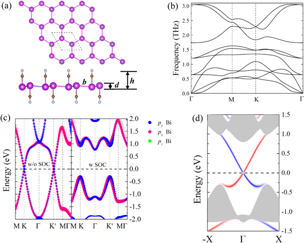
Figure 1. Geometric and electronic structures of Bi2(CN)2. (a)T op and side view of geometric structures of Bi2(CN)2 monolayer, with the bond length b for Bi-Bi, h for Bi-C and the buckle distance d. The violet, brown and white balls represent Bi, C and N atoms respectively. (b) The phonon dispersion relation. (c) Energy band structure near Fermi level without (left) and with (right) SOC interaction. The pink/blue/green dots denote px/py/pz of Bi dominated orbitals. The size of dot denotes the weight of projection. (d) Spin observed edge states of semi-infinite zig-zag Bi2(CN)2 ribbon. Gray area illustrates the bulk bands, and red/blue colors denote spin up/down helical edge states.
Download figure:
Standard image High-resolution image
Figure 2. (a) Side view of geometric structure of Bi2CN, with Bi-Bi bond length b, Bi-C distance d, buckle distance h and the buckling angle α. (b) Energy band structure near the Fermi level without (left) and with (right) SOC interaction. The blue/green dots denote pxy/pz orbitals of unsaturated Bi, and the orange dots denote pxy orbitals of Bi saturated. The size of dot denotes the weight of projection.
Download figure:
Standard image High-resolution image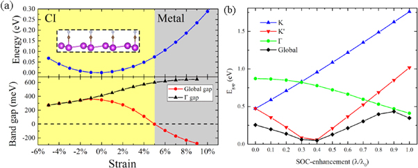
Figure 3. (a) Relative energy (top) and band gap (bottom) of Bi2CN as a function of strains. The CI (Chern insulator)-metal transition occur at a strain of  . Blue dots show the relative energy of structures under different strains, and red/black dots denote global and Γ-point gap. (b) Band gaps at K (blue),
  (red), Γ (green) points and the global gap (black) as functions of SOC strengths.
Download figure:
Standard image High-resolution imageFigure 1(c) illustrates the electronic band structures of the Bi2(CN)2 film without and with SOC. Without considering SOC, there are Dirac cones at K and  points near Fermi level, similar as pz orbits in graphene. However in Bi2(CN)2, the states around Fermi level are mainly contributed by Bi
  orbitals instead, see figure 1(c). And their 6pz orbitals (denoted in green dots) are completely saturated by cyano-groups. The system has the px and py orbitals degenerate due to the D3d rotation symmetry of the configuration. The Fermi level is located in the Dirac cones at K(
 ) point, resulting in a zero-gap semiconductor. When SOC is turned on, as shown in the right panel of figure 1(c), the valence band maximum remains at K(
 ) point, while an open of indirect band gap up to 1.10 eV appears, which is the largest value in decorated bismuthene [19] to date. Corresponding HSE calculation, shown in figure S2(a), gives similar band structure with only band gap increasing to be 1.3eV. The band gap induced by SOC indicates the possibility of 2D TI phase. For identification, we calculate Z2 topological invariants employing technique developed by Yu et al [38], see the computational details and figure S1 in supplementary material. The result gives
  , indicating that the topologically is nontrivial. Additionally, the existence of helical edge states with the spin-momentum locked by time-reversal symmetry (TRS) is plotted in figure 1(d). A gapless edge states (red/blue color shows the spin up/down of each band) appear inside the band gap of bulk, cross at Γ, and connect the top of valence band and the bottom of conduction band. Clearly that the pair of edge states are counter-propagating which carry opposite spin polarizations, which is a direct proof of QSH effect. However, unlike the SnCN, there is no band inversion observed, therefore the parity inversion mechanism can not be applied here.
4. Quantum anomalous Hall states in half-cyanided bismuth bilayer
As is known, the QSH state can be regarded as a pair of QAH states coupled by TRS, therefore, to realize a QAH state, spin polarizations should be introduced into Bi2(CN)2 to break the TRS, and turn 2D TI into CI. One of the most simple and effective ways is to completely remove CN groups of Bi2(CN)2 from one side but keeping the other side cyanided. This half-cyanided bismuthene, labelled as Bi2CN, is possibly synthesized in experiments by exposing only one side of Bi film to the reactant (cyanide source) with the other protected by the substrate. It is known that four necessary conditions [39] must be satisfied concurrently for QAH effects:
(1) 2D geometries. The geometric structure of Bi2CN is plotted in figure 2(a), with a quasi-planar 2D configuration and buckling angle  . Comparing this with a full-cyanided bismuthene, the ground state constant lattice of Bi2CN reduces to 5.37 Å, while the Bi-Bi/Bi-CN bond length remains the same. The buckle distance increases to be 0.783 Å. Bader analysis gives a charge transfer from Bi to CN by 1e, and the formation energy is up to −1.85 eV, indicating a stable chemical bond.
(2) Insulating bulk gap. Figure 2(b) gives the band structure of Bi2CN without and with SOC. When SOC is turned on, the band gap increases from 0.257 eV to 0.348 eV, indicating an insulating bulk behaviour at high temperature. The valley divergence of band structure between K and  is induced by the coaction of internal spontaneous magnetization splits, intrinsic SOC and intrinsic Rashba SOC, similar as Bi2H demonstrated by Liu and Yao et al [23].
Furthermore, the gap of Bi2CN could be tuned by external strains and SOC strengths. Figure 3(a) gives the band gaps as a function of bi-axial strain. The tensile strain here is defined as  , where a0 is the lattice constant of equilibrium state, compared to the compressed/stretched lattice a. At ground state, Bi2CN is an indirect gap insulator, with the bottom of conduct band at Γ, while the top of valence band between
  and M. Under a compression greater than
  , it becomes a direct gap insulator with a decreasing band gap and stronger compressions. Inversely when stretched, the band gap moves away from Γ and decreases to be zero at a strain of
  . With stronger stretch applied, the band gap becomes negative, resulting in a CI-Metal phase transition. Figure 3(b) gives the band gap as a function of SOC strength
  , which is artificially set partial fractions of the original SOC strength
  . In experiments it could be realized by doping lower-weight elements and applying external electric fields. Clearly the band gap at
  decreases to zero when
  , and then opens again, while at K it is monotone increasing, illustrating a valley topological phase transition only at
  .
.
(3) Ferromagnetic ording. Bi2CN has a  net magnetic moment in the cell, displaying a ferromagnetic ordering. According to the spin charge distribution in figure S3(c), we find this spin polarization comes from the local magnetic moment on the uncyanided Bi atom, attributed to the unpaired pz electron. The magnetic anisotropy energy (MAE), which is defined as MAE =
  meV, shows that the easy magnetization axis points out of the plane. The in-plane magnetization could close the band gap, indicating that Bi2CN is not robust against the direction of magnetization. The Curie temperature is estimated in a mean field(MF) method that
  , where
  , z = 6 for triangular lattice, kB is the Boltzmann constant, and
  is the effective nearest-neighbor exchange coupling in the spin model
  .
.  is calculated by the energetic difference between FM and AFM states, and it is 12 meV for Bi2CN, corresponding to
  K. Considering the empirical relation
  , we estimate a TC = 164K, which is close to that of half-iodinated stanene Sn2I [22] and higher than the liquid nitrogen temperature (77 K).
(4) Non-zero Chern number. To further identify QAH states in Bi2CN, a calculation on Chern number is necessary. The physical meaning of Chern number is the number of chiral edges near Fermi level, and this topological index could be calculated by the Chern theorem described in the supplementary material.
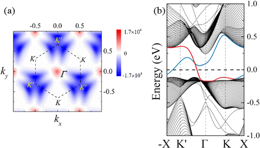
Figure 4(a) shows the Berry curvatures Ω as a function of  in the momentum space, with red-white-blue color map indicating
  from positive to negative values. When SOC is not considered, the Berry curvature distribution, plotted in figure S4, is located in the vicinity of K and
  , while with opposite signs, indicating a valley-polarized topologically trivial character. The result shows a six-fold rotational symmetry, while
  for the missing of inversion symmetry. When SOC is turned on however, the distribution on K point almost goes to zero, while a positive Berry curvature arises on Γ point. Besides,
  has negative peaks on each
  point instead, which splits into three sub-peaks like those in Kagomé model [40], for the multiple maxima in the highest occupied bands. Finally the Chern number with SOC from the integration of Berry curvature in the first BZ gives a value of −1.
Figure 4. (a) The Berry curvature with SOC in the momentum space. The red-white-blue color gives distribution of Berry curvature from positive to negative value in arbitrary unit, and the black dash lines show the first BZ. (b) Calculated band structure of zig-zag Bi2CN nanoribbon with SOC. The Fermi level is represented by the black dash line. Red (blue) lines indicate the states located at different edges.
Download figure:
Standard image High-resolution image
Moreover, the edge states for a zig-zag ribbon of Bi2CN is given in figure 4(b). The bands in blue and red are chiral edge states located at different edges, both of which cross the Fermi level in the vicinity of the  valley, which verifies the non-zero valley Chern number at
  while CK = 0. Clearly the number of chiral edge states is one, supporting the results of non-zero Chern number obtained above.
Considering the chemical similarity between halogens and the CN group, the different bulk behaviors between Bi2X and our Bi2CN is mainly from the distinction in the buckled geometry of Bi backbone. As is mentioned by Yao et al [23], a slightly buckled geometry could remarkably magnify the size of gap. Bi2CN has obviously longer Bi-Bi bond length and larger buckling distance than those of Bi2X. The former increases the localization of bands near Fermi level, and the latter increases the buckling angle which could enhance the first-order SOC strength  and then the band gap induced by intrinsic SOC [41].
For the applications of devices, it is important to choose a proper substrate material which could preserve the topological properties of Bi2CN. Considering the lattice matching, we find MoS2 ( ) a good candidate, which could fit half-cyanided bismuthene nicely with a lattice mismatch of less than 2%. With a good alignment of band gaps, it forms a van der Waals interaction with Bi2CN and preserves its bulk insulating. The geometric and electronic configurations are given in figure S5 in the supplementary material.
5. Conclusions
In summary, we perform the first-principles calculations to predict a novel QSH insulator Bi2(CN)2 which has a giant gap up to 1.10 eV. The open of band gap is mainly contributed by SOC effect. The topological characteristic is identified by Z2 invariant as well as the helical edge states. Furthermore, the corresponding half-cyanided bismuthene Bi2CN is found as Chern insulator supporting QAH states, with a large band gap of 0.348 eV and a Curie temperature up to 164 K. It is identified by Chern number as well as the chiral edge states. The band gap can be further engineered by the applications of bi-axial strains. Therefore, the BiCN family is an appropriate and flexible candidate material for spintronic and valleytronic devices.
Acknowledgments
We would like to thank Dr Hong-bin Zhang for useful discussions. This work was supported by the National Natural Science Foundation of China (Grant No. 11274143, 11434006, 61172028, 61504048 and 11304121), the Natural Science Foundation of Shandong Province (Grant No.ZR2013AL004, ZR2013AL002 and BS2013CL020) and Research Fund for the Doctoral Program of University of Jinan (Grant No. XBS1433).