


Abstract
We have studied the built-in voltage in heterostructures composed of ferroelectric PbTiO3 and dielectric spacers of SrTiO3, grown on SrTiO3 substrates with SrRuO3 bottom electrodes. We used piezoresponse force microscopy to determine the domain structure of the samples and perform local switching experiments. By increasing the thickness of the SrTiO3 spacer layers, we were able to tune the polarization configuration in the PbTiO3 films by gradually going from a monodomain configuration to a polydomain one. The built-in voltage was found to be linked to the choice of electrodes and to the thickness of the spacer layer. The stability of artificially poled regions was also affected, with a faster back-switching for the samples with the thicker SrTiO3 spacers. We have additionally compared samples with and without a top SrRuO3 electrode, showing that a top electrode layer results in a stronger built-in voltage, responsible for a preferential monodomain configuration and a very fast back-switching of artificially poled regions.
Export citation and abstract BibTeX RIS

Original content from this work may be used under the terms of the Creative Commons Attribution 3.0 licence. Any further distribution of this work must maintain attribution to the author(s) and the title of the work, journal citation and DOI.
General description of effective screening/depolarization field and built-in field
Given the recent progress in the growth of oxide heterostructures and ultrathin films, it is possible to create artificially layered materials with atomically precise interfaces. In such systems, the effects of these interfaces, and of the surface, are extremely important [1], motivating the ongoing search for novel phenomena appearing and the exponential growth of the field of oxide interface engineering [2, 3]. In electronic devices based on functional oxides, and in particular on ferroelectrics, the interface between the oxide thin film and the electrode(s) is also crucial from a technological viewpoint. For novel device concepts such as ferroelectric tunnel junctions and memristors [4–8], understanding and quantifying the effects of the electrostatic boundary conditions in nanoscale ferroelectrics is becoming more important than ever.
It is well established that the switching properties of ferroelectric films depend on the specific ferroelectric-electrode system chosen [9], and that polarization stability is determined by the screening of surface/interface bound charges [10]. The origin of this dependence of the ferroelectric state of a thin film on the electrostatic boundary conditions is linked to Fermi level alignment and related band-bending, depletion region, space charge, and other phenomena. Other factors can play a role too. For example, it was shown by Stengel et al that ferroelectricity can be either destabilized or enhanced at metal-oxide interfaces, depending on the stiffness of the electrode-oxide bonds [11]. All these effects result in built-in voltages and depolarization fields that affect the stability of the polarization and the intrinsic domain structure [12].
The built-in voltage leads to a built-in field whose intensity depends on the ferroelectric film thickness. Considering the 'intrinsic' ferroelectric energy double well and polarization-electric field (P-E) loop illustrated in figure 1 (red), the built-in field asymmetrizes the energy double well, leading to a favored polarization direction, and shifts the P-E loop horizontally (green).
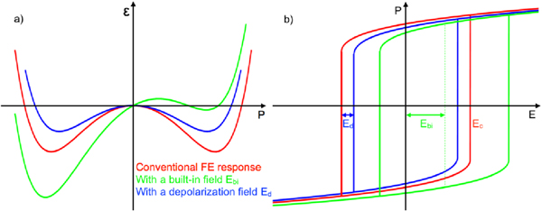
Figure 1. (a) Double-well energy ε(P) and (b) P-E loop showing the conventional ferroelectric response (red). The effect of a built-in field Ebi is to asymmetrize the energy double-well and to shift the whole P-E loop (green). A depolarization field Ed makes the double-well shallower and shrinks the P-E loop, reducing the coercive voltage Ec (blue).
Download figure:
Standard image High-resolution imageThe depolarization field, produced by imperfectly screened surface bound charges, becomes important as the film thickness is reduced. This field depends on the effective screening length of the particular interface  , on the ferroelectric film thickness d, and on the polarization P as [13]
  . This depolarization field is always oriented opposite to the polarization, thus destabilizing the polarization state, making the energy double-well shallower and reducing the opening of the P-E loop (figure 1-blue). Considered most of the time as detrimental to the properties of ferroelectric thin films, it can have the positive effect of reducing the voltage needed to switch the polarization [14].
We recently studied the effect of introducing dielectric layer spacers between ferroelectric thin films and the electrode layers[12]. The main idea was to use these dielectric layers (made of SrTiO3) as a way to tune the effective screening length and thus the depolarization voltage and field. Using piezoresponse force microscopy (PFM), we could show that the domain structure evolves from monodomain for PbTiO3 films grown on SrTiO3 substrates with an SrRuO3 electrode without dielectric spacers, to polydomain as the spacer layer thickness is progressively increased to a few nanometers. Here, we use the same approach to investigate the effect of electrodes and spacer layers on the built-in voltage and field. The samples studied are PbTiO3 thin films of varying thicknesses (up to 50 nm), grown on SrTiO3 substrates with a bottom SrRuO3 electrode of 22 nm. Two series of samples were produced, one without a top electrode, where surface adsorbates are the source of screening, and one with a top SrRuO3 electrode. For both series, we have used SrTiO3 top and/or bottom spacer layers of different thicknesses (from 0 to 10 unit cells, i.e. 4 nm). To probe the built-in voltage in both types of samples and study the effect of the spacer layer thickness on the intrinsic domain configuration and on the domain stability, we have used PFM coupled with structural characterization. Our observations demonstrate that both mechanisms, i.e. the built-in voltage and the depolarization field, can play a role simultaneously, with a progressive change from a state where the intrinsic domain configuration is governed by the internal bias field towards a state where the domain configuration is governed by the depolarization field alone, on increasing the spacer layer thickness (see Supporting Information for more details).
Determination of the built-in voltage
To estimate the built-in voltage in our samples, we performed local switching measurements using PFM [15–17]. Amplitude and phase signals were recorded using an Asylum Research Cypher atomic force microscope (AFM) operating in dual resonance tracking (DART) mode [18], while a DC voltage VDC was ramped between the top and bottom electrodes. For samples without a top electrode layer, the conducting tip itself served directly as a top electrode. For samples with a top electrode layer, the voltage was simultaneously applied to the top electrode (via an external wire) and to the tip, in order to avoid any electrostatic effect. One advantage of this technique over techniques based on the integration of switching currents is that it is much less sensitive to leakage.
Built-in voltage in samples without a top electrode layer
On the series of samples without a top electrode layer, the built-in voltage was measured using switching spectroscopy piezoresponce force microscopy (SSPFM), as described in [19]. The set-up is represented in figure 2(a): a DC bias VDC is applied to the AFM tip in addition to the AC probing voltage VAC, and the bottom electrode is grounded. The PFM phase and amplitude are then recorded while the DC bias is ramped stepwise, going back to zero bias after each step, as schematically shown in figure 2(b). This produces two measurements: one as a function of the bias applied at the time of the acquisition ('on'), and one as a function of the bias applied just before the acquisition ('off'). To avoid effects of electrostatic interactions between tip and sample, only the results of the 'off' state are used. This produces the typical loop shape for the phase, and a butterfly shape for the amplitude as shown on figure 2(c) for a 50 nm PbTiO3 film with a 2 nm top SrTiO3 spacer and a 22 nm SrRuO3 bottom electrode. To make our measurements more reliable, they were repeated a large number of times on a grid (typically at least 16 × 16 points evenly spaced on a 2 × 2  grid). The switching biases were then extracted as the points of lowest amplitude, and used to calculate the built-in voltage for each point, corresponding to the value of VDC at the center of the loop1
. An example of such a grid of values is shown in figure 2(d).
grid). The switching biases were then extracted as the points of lowest amplitude, and used to calculate the built-in voltage for each point, corresponding to the value of VDC at the center of the loop1
. An example of such a grid of values is shown in figure 2(d).

Figure 2. Switching spectroscopy piezoresponce force microscopy (SSPFM) used to determine the built-in voltage in a sample. (a) Representation of the set up. (b) Sketch of the signal used to obtain the SSPFM loops. (c) Phase and amplitude measured after applying a DC bias VDC to a B-doped diamond tip on a 50 nm PbTiO3 film with 2 nm top SrTiO3 spacer and 22 nm SrRuO3 bottom electrode. The phase displays the expected hysteresis loop, with the butterfly loop for the amplitude, showing a built-in voltage of 1.6 V. By repeating these measurements at different locations on a sample, a grid is obtained allowing the evaluation of the averaged built-in voltage of the sample (d). The values are quite homogeneous, except for a spot on the top right, which could be explained by the presence of an impurity on the sample surface.
Download figure:
Standard image High-resolution imageThe phase and amplitude loops are all systematically shifted towards positive bias, corresponding to a residual field in the ferroelectric layer pointing up, resulting in a preferred up polarization.
The measurements were performed using two different kind of tips: NSC18 Cr–Au coated silicon tips from MikroMasch and B-doped diamond tips from NaDiaProbes. It is worth noting that the values are different when the measurements are performed with different kind of tips. The additional AFM-tip/ferroelectric interface itself modifies the built-in bias, so that the values measured are for the whole system including the ferroelectric layer, the surrounding layers and the electrodes/tip. It is then possible to compare the values obtained for different samples under the same conditions when using the same tip.
The evolution of the built-in voltage has been studied as a function of the thickness of the SrTiO3 layers, for two different series of samples, one with 50 nm thick PbTiO3 layers, and one with 20 nm thick PbTiO3 layers, and with two different kind of AFM tips, as reported in table 1.
Table 1. Built-in voltages reported for different samples without top electrode, with different PbTiO3 and SrTiO3 thickness and using different AFM tips.
| PbTiO3 thickness (nm) | SrTiO3 thickness (top/bottom, when different) (nm) | Built-in voltage measured with Cr/Au coated tip (V) | Built-in voltage measured with B-doped diamond tip (V) |
|---|---|---|---|
| 10 | 2 | 0.31 ± 0.17 | |
| 0 | 1.33 ± 0.32 | ||
| 0.4 | 1.48 ± 0.31 | 1.62 ± 0.40 | |
| 20 | 0.8 | 0.88 ± 0.15 | 0.89 ± 0.28 |
| 2 | 1.71 ± 0.23 | ||
| 2 | 1.14 ± 0.28 | 1.27 ± 0.30 | |
| 4 | −0.27 ± 0.44 | 0.60 ± 0.13 | |
| 0 | 1.12 ± 0.36 | ||
| 2 / 0 | 1.75 ± 0.45 | ||
| 50 | 0 / 2 | 0.58 ± 0.51 | |
| 2 | 0.32 ± 0.47 | ||
| 2 | 0.38 ± 0.67 |
50 nm series
Figure 3 shows the results for a series of four samples consisting of a 50 nm PbTiO3 film with a top and/or bottom SrTiO3 spacer of 2 nm (5 u.c.). The samples without a bottom spacer (A and D) are monodomain up, while those with a bottom spacer (B and C) are polydomain (up background with down nanodomains), independently of the top spacer, as shown in [12].

Figure 3. Built-in voltage in the 50 nm PbTiO3 series. Top: schematic representations of the four samples measured (A–D), with the PFM phase measurements showing the intrinsic domain configuration (A and D are monodomain, while B and C are polydomain) [12], and an example of a switching loop obtained locally for each sample using a B-doped diamond tip. Bottom left: x-ray diffraction measurements for each sample (shifted for clarity), showing how the c-axis of the PbTiO3 varies depending on the intrinsic domain configuration (from [12]). Bottom right: measured built-in voltage, averaged over a large number of measurements as described in the text, versus c-axis of PbTiO3. Both the built-in voltage and the c-axis clearly vary depending on the intrinsic domain configuration, with larger values for the monodomain samples compared to the polydomain ones.
Download figure:
Standard image High-resolution imageA positive built-in voltage is observed for all the samples, consistent with the observed preferential direction of polarization. The built-in voltage correlates with the c-axis values measured via x-ray diffraction (see figure 3). Samples A and D are monodomain with a larger built-in voltage that results, under zero applied bias, in an increase in their polarization, associated with an increase of the c-axis due to polarization-strain coupling. On the other hand, samples B and C are polydomain, as a result of a stronger depolarization field that would be present in these samples if they were monodomain. In these samples, the built-in voltage is smaller, leading to a reduced piezoelectric distortion. Moreover, the domains with an up polarization would experience an increase in their c-axis, while the opposite domains would have their c-axis decrease. It is most certainly the presence of domain walls in the polydomain configuration that explains the observed reduced tetragonality, as domain walls are paraelectric and correspond therefore to a reduced distortion. As mentioned in [12], Takahashi et al [20] also observed such an increase of the c-axis lattice parameter for monodomain PbTiO3 films grown directly on Nb-doped SrTiO3 substrates compared to polydomain ones, upon using photochemical switching to induce the polydomain to monodomain transition.
20 nm series
The other series of samples is composed of a 20 nm PbTiO3 film with symmetric SrTiO3 spacers of different thicknesses, from 0 up to 10 unit cells (see schematic representation in figure 4). These samples were shown to be monodomain for the samples with 0 and 1 unit cell of SrTiO3 and polydomain for thicker spacers [12]. Figure 4 shows the built-in voltage measured with two different tips, a B-doped diamond tip (black dots) and a Cr/Au coated silicon tip (red squares). The results obtained with both kinds of tips demonstrate that the built-in voltage decreases for the sample with the thickest SrTiO3 spacers. This observation can be compared to the study by Lu et al [21]: in BaTiO3 thin films with SrRuO3 top and bottom electrodes, they also observed a reduction of the built-in field by adding 2 unit cells of SrTiO3 between the film and the top electrode. This was attributed to the symmetrization of the chemical interface termination sequence. The RuO2/BaO interface termination sequence occurring naturally at the top interface seems to be detrimental due to the presence of a pinned interface dipole arising from a mismatch between ionic radii. By adding the SrTiO3 layer, the unfavorable interface termination is eliminated, leading to a stable and switchable ferroelectric polarization. The insertion of the SrTiO3 also results in a further enhancement of the ferroelectric stability.

Figure 4. Built-in voltage as a function of SrTiO3 spacer thickness for the samples with 20 nm of PbTiO3, measured with a B-doped diamond tip (black dots) and with a Cr/Au coated silicon tip (red squares). The dotted line delimits the transition from a monodomain to a polydomain configuration, as seen in the corresponding PFM images from [12], with the phase in brown (right) and the amplitude in blue (left). The results obtained with both kinds of tips indicate a decrease in the built-in voltage for the sample with the thickest SrTiO3 spacers. Additionally, the built-in voltage measured with a Cr/Au coated silicon tip is systematically lower than that measured with a diamond tip, demonstrating the effect of the tip itself. Inset: representation of the samples measured.
Download figure:
Standard image High-resolution imageOur measurements additionally show that the built-in voltage measured with a Cr/Au coated silicon tip is systematically lower than that measured with a B-doped diamond tip, demonstrating the effect of the tip itself. Note that in the sample with the thickest SrTiO3 spacer, the built-in voltage measured with the Cr/Au coated silicon tip is actually negative. Here the tip directly plays the role of top electrode, and changing the tip material results in different electrical boundary conditions, therefore affecting the total built-in voltage. The measured built-in voltage is then the sum of the built-in voltage in the sample and the one due to the tip, and depending on the tip material, can actually be negative.
Built-in voltage in samples with a top electrode layer
To study the effect of a top electrode layer, a sample similar to sample C in figure 3 (50 nm PbTiO3 film with top and bottom 2 nm SrTiO3 spacers and with 22 nm bottom SrRuO3 electrode on SrTiO3 substrate) was grown, with the addition of an 11 nm top SrRuO3 electrode layer sputtered in situ and then patterned to form squares of different sizes (the one used here is 100 × 100  ).
).
PFM measurements were performed through the electrode, under different DC biases applied directly to the electrode, as described by Gruverman [22] and used by different groups (e.g., [23, 24]). In this case, we did not perform SSPFM measurements, as VDC is applied to the whole electrode, so the whole area below switches at every cycle and each point in the grid will be affected by all the measurements performed before. Instead, the domain configuration underneath the electrode was monitored on 2 × 2  scans by recording the phase and amplitude PFM response to a small AC voltage VAC while applying a DC voltage VDC to the tip and the top electrode layer. Figure 5 (left) shows some of the phase images obtained on this sample with
  . For
. For  , the region below the electrode is mostly uniformly polarized, with the polarization oriented up (a). When increasing the voltage, down polarization domains appear (b)–(d), until the region is fully down polarized at
  (e). When VDC is then progressively decreased, up polarized domains appear in the down polarized background (f). These up domains grow until they cover most of the region (g)–(i), with only a few down domains left, until finally the region is fully monodomain up at
  (j). Note also the difference between (c) and (f), both taken for
  , but one on increasing VDC and the other on decreasing it.

Figure 5. Comparison of the built-in voltage in two samples: 50 nm PbTiO3 films with top and bottom 2 nm SrTiO3 spacers and with 22 nm bottom SrRuO3 electrodes on SrTiO3 substrates, one with additionally a 11 nm top SrRuO3 100 × 100  electrode (left) and one without (right). (Left) PFM phase images obtained on the sample with the top SrRuO3 electrode with different DC bias applied to the tip and top electrode layer. Switched area proportion (number of pixels with a polarization pointing down divided by the total number of pixels) versus VDC, showing a large built-in voltage of 0.9 V in this sample (see supporting information). (Right) For comparison, a PFM phase image obtained at VDC = 0 V on the same sample but without a top electrode layer is shown together with a phase hysteresis loop and an amplitude butterfly loop obtained by SSPFM with a B-doped diamond tip, showing a built-in voltage close to 0.
Download figure:
Standard image High-resolution imageFrom each image, it is possible to extract the switched area proportion which is taken as the number of pixels with a polarization pointing down divided by the total number of pixels. This gives a value of 1 for a fully down polarized region, and 0 for up. When plotted as a function of the voltage applied to the tip and top electrode layer VDC, this results in a hysteresis loop as shown in figure 5 (left; the values for the images (a)–(j) are reported directly on this graph, together with the values obtained for other scans not shown here). This hysteresis loop is shifted and shows a built-in voltage of 0.9 V. For comparison, the phase hysteresis loop and amplitude butterfly loops obtained on the same sample but without a top SrRuO3 electrode are also shown in figure 5 (right). For this sample, the built-in voltage is close to 0 V, and the PFM phase image obtained with VDC = 0 V has a switched area proportion close to 0.5. This demonstrates that the presence of a top SrRuO3 electrode induces a built-in voltage in a sample that does not have any otherwise.
In the hysteresis in figure 5 (left), data points are displayed for different VAC values. Even for very large VAC (larger than the coercive voltage observed for this loop), the measurement does not seem to be affected. This can be explained by the fact that the PFM signals are recorded using the DART mode at a very high frequency (typically 370 kHz), so that the effective voltage applied to the ferroelectric layer is reduced by the RC time constant of the circuit. The signal period is shorter than the observed minimum switching time in similar systems (100  lower limit for one pulse switching in 270 nm thick PbZr0.2Ti0.8O3 [25]). This agrees with the work of Ivry et al [26] where high-resolution PFM imaging is achieved by using a VAC higher than the DC coercive voltage of the sample near the cantilever in-contact resonance frequency. Increasing the value of VAC however can reduce the noise level in the PFM measurements.
Effect of built-in field on intrinsic domain configuration in samples without a top electrode layer
The effect of the built-in field can also be observed in the domain configuration of the samples without a top electrode. In [12], PFM images revealed a drastic change in the intrinsic domain shape in our samples as a function of the SrTiO3 spacer thickness as well as the PbTiO3 film thickness.
50 nm series
In the series of samples with 50 nm PbTiO3 films, the samples without a SrTiO3 bottom spacer have a larger built-in voltage and are monodomain, while the two samples with a bottom SrTiO3 spacers are polydomain with a reduced built-in voltage, as shown in figure 3. The built-in voltage results in a preferential polarization orientation that corresponds to the polarization direction of the monodomain samples, and to the direction of the polarization background for the polydomain samples.
20 nm series
In the series of samples with 20 nm PbTiO3 films, the samples without SrTiO3 spacers or with very thin (1 u.c.) ones are monodomain, while they become polydomain with SrTiO3 spacer layers of 2 u.c. and more. The domains are more difficult to resolve in the polydomain samples in this series than in the 50 nm series. However, a gradual change of the phase can be seen as the SrTiO3 spacer layer thickness increases (figure 6). To quantify this evolution, two reference regions were written by applying negative or positive DC bias to the tip, resulting in two square domains with well defined polarization oriented up or down. The mean phase in the as grown region can then be directly compared to that in the switched regions for this series of samples, as shown in figure 6. For the samples with thicker spacers, the mean phase of the as-grown region is significantly higher than  , meaning that more domains of opposite polarization are present in those samples, in agreement with the observations of a lower built-in voltage. However, none of the samples shows a mean phase in the as-grown region of more than 90°, corresponding to half up, half down. This is in line with our measurement of the built-in voltage, suggesting a preferred up polarization for all these samples.
Figure 6. Averaged linesection through the PFM phase images of the five samples shown in figure 4 with 20 nm of PbTiO3 and symmetric SrTiO3 spacers of varying thickness. Two square domains were poled with opposite voltages allowing direct comparison with the as-grown polarization state. For the two monodomain samples (with 0 and 1 u.c. of SrTiO3), the phase of the as-grown region is aligned with that of the up written region, indicating a preferential up-polarized intrinsic configuration, in line with the measured built-in voltage.
Download figure:
Standard image High-resolution imageEffect of built-in field on domain stability
To further discriminate between the effect of the built-in field and of the depolarization field, it is helpful to look at the back-switching of artificially written regions. There are several ways of studying domain wall dynamics in ferroelectric thin films. One of them is using time-resolved x-ray microdiffraction, as used by Grigoriev et al on Pb(Zr, Ti)O3 thin films to follow the polarization reversal after an electrical pulse, revealing a domain wall velocity of 40 m s−1 and a strong heterogeneity of the nucleation of reversed domains [27]. Other approaches are based on direct imaging of the polarization state by PFM while a voltage is applied to the AFM tip used as a top electrode, or to a top electrode layer [22–24]. We have used PFM to follow the domain configuration and backswitching in different samples, both with and without a top electrode layer.
Without a top electrode layer
50 nm series
Figure 7 shows PFM measurements obtained on the 50 nm PbTiO3 film with 2 nm top and bottom SrTiO3 interlayers. PFM measurements on the same 1.2 × 1.2 μm2 region and under the same conditions were repeated after the area was first scanned with a DC bias applied to the tip (from −2.5 V up to +2.5 V as indicated in the figure). After applying a negative tip bias, the down polarized domains (white) shrink in size, while they expand after applying a positive tip bias. The images were not taken in that specific order, and although there is some spatial drift from one image to the other, it is possible to recognize and follow specific domains in their size alteration. Moreover, a noticeable relaxation of the domain size was observed after the poling, as shown in figure 8, with a recovery of the initial configuration after a time of typically 3 h, showing that the position of the domain wall reproducibly relaxes back to its original position. These results demonstrate that it is possible to switch locally the polarization by applying a DC voltage between the AFM tip and the bottom electrode by moving the intrinsic domain walls, with a relaxation on a time scale suitable for measurements.

Figure 7. 1.2 × 1.2 μm2 PFM phase images of the 50 nm PbTiO3 film with 2 nm top and bottom SrTiO3 interlayers. The measurements were performed on the same region and under the same conditions, directly after the area was first scanned with a DC bias applied to the tip (from −2.5 V up to +2.5 V, as indicated in the figure).
Download figure:
Standard image High-resolution image
Figure 8. Same measurements as in figure 7, but now showing the time evolution of the domains after the same area was first scanned either with +2.0 VDC or with −2.5 VDC. The images are numbered according to there acquisition after the area was first scanned with the specified voltage. The images were recorded with a speed of 0.5 Hz for 512 lines (∼17 min per scan), showing a complete recovery of the unpoled configuration after approximately 3 h. (See supporting information.)
Download figure:
Standard image High-resolution image
Figure 9. To emphasize how quickly the change in polarization configuration occurs on a sample composed of a 50 nm PbTiO3 film with 2 nm top and bottom SrTiO3 interlayers and top (11 nm) and bottom (22 nm) SrRuO3 electrodes, PFM phase is measured continuously along the same line (2 μm length). While scanning, different DC voltages are applied to both the tip and top electrode layer. The horizontal scale is the measurement time, with a reading frequency of 1 Hz. The dotted red lines show the time at which the DC voltage is changed to the value indicated above.
Download figure:
Standard image High-resolution image
20 nm series
Polarization back-switching was also studied in the series of samples with 20 nm PbTiO3 films by using the same procedure as described above to follow the evolution of written regions as a function of time and are shown in [12]. Measurements of the retention time of the written polarization (up and down) regions show a rather different mechanism for different SrTiO3 spacer thicknesses. Without any SrTiO3 spacer, the domain wall of the written structure moves and deforms with time, reducing the extension of the written region, but keeping the full amplitude of the switched region bounded by the domain wall. This mechanism can be explained by the presence of a built-in-field pushing towards a preferential orientation state, with the back-switching occuring at the domain wall. On the other hand, with increasing thickness of the SrTiO3 spacers, the back-switching mechanism is rather different with nano-domains appearing within the written region. This mechanism, changing a monodomain region towards a polydomain configuration, can be attributed to the depolarization field. For the sample with SrTiO3 spacer layers of just 1 u.c., both effects can be seen: the roughening of the domain wall delimiting the written region as well as the appearance of opposite nano-domains inside, attesting that both mechanisms, i.e. the built-in voltage and the depolarization field, can play a role simultaneously.
With a top electrode layer
When adding a top electrode layer to these samples, we noticed that not only the domain configuration is changed and the loop is more shifted, but also the back-switching is much faster. To emphasize how quickly the change in polarization configuration occurs on a sample composed of a 50 nm PbTiO3 film with 2 nm top and bottom SrTiO3 interlayers and top (11 nm) and bottom (22 nm) SrRuO3 electrodes, PFM phase is measured continuously along the same line (2 μm length) (figure 9). While scanning, different DC voltages are applied to both the tip and top electrode layer. The horizontal scale is the measurement time, with a reading frequency of 1 Hz. The dotted red lines show the time at which the DC voltage is changed to the value indicated above. The domain configuration changes abruptly at each modification of the DC voltage, with almost no evolution as a function of time for a constant DC voltage. These measurements also show the uniform up polarization state for  and uniform down polarization state for
  . This is in line with the shifted loop shown in figure 5 for the same sample.
Note also that even upon complete switching, the opposite domains always start to nucleate at the same position, proving again the presence of strong nucleation sites, both for up and down domains. This is very much in line with the observations of Kim et al [23] or Jesse et al [28], who demonstrated the presence of preferential nucleation sites in Pb(Zr, Ti)O3 capacitors using PFM measurements.
Conclusion
When working with ferroelectric ultrathin films, the boundary conditions are crucial to determine the properties of the ferroelectric layer. In this work, we have shown how it is possible to tune both the depolarization field and the built-in field by adding spacer layers between the ferroelectric film and the screening charges (electrode or surface adsorbates). SSPFM measurements revealed a progressive decrease of the built-in voltage as the thickness of the SrTiO3 spacers increases. By increasing the thickness of the SrTiO3 spacers layers sandwiching PbTiO3 thin films, we were also able to tune the polarization configuration, gradually transitioning from a monodomain configuration with a preferential up polarization towards a polydomain one with down-polarized domains in an up-polarized background. The stability of the written regions was also affected by the SrTiO3 spacer thickness, with a faster back-switching for the samples with the thicker SrTiO3 spacers. Throughout this work, we have also compared series of samples with and without a top electrode layer, showing that a top SrRuO3 electrode results in a stronger built-in voltage, responsible for a preferential monodomain configuration and a very fast (less than 1s) back-switching of oppositely written domains.
In view of recent work on controlling the dynamics of domains and domain walls by engineered pinning/nucleation defects and electrode modification [29–34] for possible nanoelectronics applications, understanding the significant contribution of these boundary condition effects is especially useful. The simple method used here to control the domain structure and dynamics offers not only an excellent tool for fundamental studies of ferroelectric nanodomains and polarization stability in ferroelectrics but may also be used to enhance the dielectric properties of ferroelectric thin films by exploiting the large domain wall contributions to the dielectric permittivity [35], for modulating the velocities of domain wall displacement [34], or to engineer materials whose properties are dominated by the exotic functionalities that have recently been discovered at ferroic domain walls [36]. We thus believe our work is extremely timely and will open an original new research direction within this large and technologically important field.
Footnotes
- 1
If switching did not take place, for example if the contact between tip and sample was bad due to impurities on the sample surface or tip degradation, this routine will give random results. These points are therefore filtered out, and the mean and standard deviation of the remaining values are used to calculate the average built-in voltage of the sample under study.