


Abstract
We present an all-dielectric photonic crystal structure that supports two-dimensionally confined helical topological edge states. The topological properties of the system are controlled by the crystal parameters. An interface between two regions of differing band topologies gives rise to topological edge states confined in a dielectric slab that propagate around sharp corners without backscattering. Three-dimensional finite-difference time-domain calculations show these edges to be confined in the out-of-plane direction by total internal reflection. Such nanoscale photonic crystal architectures could enable strong interactions between photonic edge states and quantum emitters.
1. Introduction
Topology is a ubiquitous concept in physics, ranging from electrons in solid state [1, 2], quantum degenerate gases [3, 4], and sound [5–8]. A key manifestation of topological physics is the presence of edge modes which are robust to local disorder. The prospect of using topological photonic materials for such robust propagation of light has attracted a great deal of interest [9, 10].
Topologically protected edge states have been experimentally demonstrated in systems at microwave freqencies [11, 12] and optical frequencies, specifically in ring resonators [13, 14], and in coupled waveguides [15]. Subsequent work measured the invariants characterizing the topology of two-dimensional photonic systems [16]. Embedding quantum emitters into these optical frequency devices could generate strong optical nonlinearities that exhibit new physical behavior. Theoretical work has shown that the interplay between emitters and chiral states results in intriguing phenomena such as many-body position-independent scattering [17], dimerization of driven emitters [18] and fractional quantum Hall states [19–21].
Strong light–matter interactions with optical emitters usually require the concentration of light to small mode-volume nanophotonic devices [22]. Two-dimensional photonic crystals are one of the most promising nanophotonic platforms for this application because they confine light to less than an optical wavelength [23, 24]. Recently, several works have proposed photonic crystal structures where deformations open a gap in the Dirac cone dispersion to achieve non-trivial topological bands [25–29]. Notably, a C6v symmetry-protected lattice was utilized in [25] to realize a topological photonic crystal where concepts such as photonic topological bands and pseudo-time-reversal symmetry were studied in detail. However, these proposals either make use of dielectric cylinders, which make it difficult to experimentally achieve out-of-plane confinement in planar all-dielectric nanophotonic systems, or make use of metallic mirrors to achieve out-of-plane confinement, which is undesirable for devices operating at optical frequencies where loss in metals is significant. Thus, it would be highly desirable to create an all-dielectric topological photonic crystal which is confined in the out-of-plane direction without the use of metal.

Inspired by the results of [25], here we present an all-dielectric topological photonic crystal design that exhibits two-dimensional edge states confined by total internal reflection in a dielectric slab, enabling low-loss confinement of light in the third-dimension. This structure addresses the challenge of experimentally realizing topological photonic crystals and enabling strong interactions with optical emitters. Our system exhibits spin quantum Hall physics for pseudo-spin photonic polarizations. As a result of time-reversal symmetry, the edge states are helical: edge states of opposite helicity travel in opposite directions. We utilize a honeycomb periodic structure with six-fold symmetry based on triangular holes. This structure ensures a complete bandgap for transverse-electric-like (TE-like) modes. Deformations of the unit cell that preserve its rotational symmetry change the topology of the structure. We show that interfacing two materials of different band topologies results in robust two-dimensionally confined edge states that can propagate around sharp bends.
2. Photonic crystal design and band structure
Figure 1 shows a schematic of our photonic crystal structure. The starting point is a honeycomb lattice made of equilateral triangular holes in a dielectric material as shown in figure 1(a). We can view this system as a triangular lattice with a basis consisting of two triangular holes, as is typically done in studies of graphene [30]. The black outline shows such a two-hole unit cell. Figure 1(b) shows the first Brillouin zone (dashed line), which is a hexagon. We denote the high-symmetry points [31] by Γ, and . Alternatively, we can also view this structure as a triangular lattice of six-hole unit cells (white dashed hexagons in figure 1(a) which we call honeycomb clusters), where the relevant parameters are the lattice constant of the triangular lattice a0, the distance between the center of each cluster to the centroid of each triangular hole R, the length of each side of the equilateral triangular holes s, and the height of the dielectric material h. In the honeycomb lattice, the relationship holds. Figure 1(b) shows the first Brillouin zone as a solid hexagon and Γ, M and K indicate the high symmetry points. Note that the first Brillouin zone for the six-hole unit cell is smaller than for the two-hole unit cell due to the larger real space unit cell area.


Figure 1. Schematic of our proposed honeycomb-lattice-like photonic crystal. (a) Baseline structure of equilateral triangular holes arranged in a honeycomb lattice in a dielectric material. This honeycomb lattice can be viewed as a triangular lattice of two-hole unit cells (black solid rhombus), or alternatively as a triangular lattice of six-hole unit cells (white dashed hexagons), which we call honeycomb clusters with . (b) First Brillouin zones for the six-hole (solid) and two-hole (dashed) unit cells. The letters indicate high-symmetry points. (c) (and (d)) Same structure as in (a) except that (, which we call shrunken (expanded) clusters.


Download figure:
Standard image High-resolution imageWe first analyze the band structure of this photonic crystal in the two-hole unit cell picture using three-dimensional numerical finite-difference time-domain calculations (Lumerical FDTD Solutions). We perform simulations using GaAs as the dielectric substrate, with index of refraction taken from [32]. The parameters we use are , s = 140 nm, and h = 160 nm, which are typical dimensions for photonic crystal structures [33–35]. We focus on the TE-like modes of the system where the electric field at the symmetric plane of the system lies in-plane. Figure 2(a) shows the band structure of the honeycomb lattice corresponding to figure 1(a) along the high-symmetry points of the Brillouin zone. The gray region indicates the portion of the band structure above the light line where there are no guided modes confined in the dielectric material of finite thickness [36]. There is a Dirac point at the point, indicated by the red arrow in figure 2(a), located below the light line. Near this Dirac point, we can modify the topological properties of the photonic crystal by changing the ratio [25]. However, these perturbations also change the symmetry of the lattice and so we can no longer use the rhombus-shaped two-hole unit cell to construct the band structure. Instead, we use the hexagonal six-hole unit cell to construct the band structure without destroying the rotational symmetry of the system.


Figure 2. Band structures show opening and closing of a band gap around the Dirac point as we perturb the lattice. (a) Band structure of the honeycomb lattice in the two-hole unit cell picture. The gray area represents the region above the light line, where light can leak out of the plane. A Dirac point exists at the point (red arrow) and is below the light line. (b)–(d) Band structure calculated with the six-hole unit cell with honeycomb clusters (), shrunken clusters (), and expanded clusters () respectively. The red arrow indicates the Dirac point, and the green areas represent the band gap.


Download figure:
Standard image High-resolution imageWe obtain the band structure for the six-hole unit cell by appropriate band folding of the bands obtained from the two-hole unit cell6 . Although both Brillouin zones share the same Γ point, the and points for the two-hole unit cell [30] become folded over onto the Γ point of the six-hole unit cell to form a doubly degenerate Dirac point at 319 THz (which corresponds to 940 nm) as indicated by the red arrow in figure 2(b).


We perturb this system by varying R with respect to a0 to get clusters that are shrunken () or expanded () as shown in figures 1(c) and (d) respectively. Figures 2(c) and (d) show the corresponding band structures specifically for and respectively. Increasing or decreasing the ratio about the honeycomb lattice opens a band gap at the Dirac point. In particular, the band gaps are 13 and 25 THz wide for the shrunken and expanded clusters respectively. By comparing the eigenstates at the Γ point for the expanded and shrunken structures, we see that the eigenstates are inverted between the two structures, indicating that the band topology changes as we tune the ratio (see footnote 7). In particular, the expanded structure gives rise to a non-trivial band topology whereas the shrunken structure leads to a topologically trivial band gap (see figure 4(a) in (see footnote 7)).


To further confirm the numerically observed band inversion, we also analytically study the system with a tight-binding model (see footnote 7). The Hamiltonian of our system reduces to the Bernevig–Hughes–Zhang model for the quantum spin Hall effect [37], where the mass term changes sign when the clusters are shrunken and expanded around . Consequently, the bands acquire non-zero Chern numbers that are the direct indication of non-trivial band topology. In this case, the polarization profile of the in-plane electric field acts as the pseudo-spin (see footnote 7).

3. Two-dimensionally confined topological edge states
Non-trivial band topologies manifest themselves most dramatically in the form of guided topological edge states at the boundary between two gapped regions that have different band topologies. To confirm this, we perform three-dimensional simulations of the structure schematically shown in figure 3(a) using the same values for the parameters a0, s and h as previously. We examine topological edge states at an interface between one region composed of unit cells with shrunken clusters (13 clusters wide) and another region of expanded clusters (12 clusters wide). These two regions share a common band gap in bulk as shown in figures 2(c) and (d).
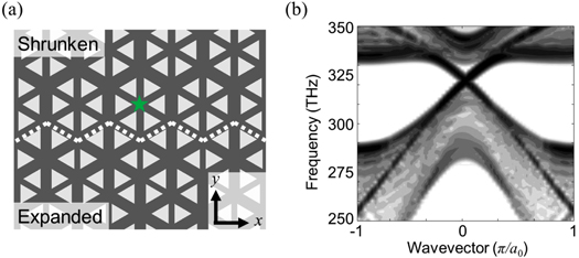
Figure 3. Schematic and band structure which gives rise to topological edge states. (a) Schematic of two regions with different band topologies. White dotted line marks the boundary between the two regions. The star (green) indicates the location where we placed a circularly polarized electric dipole to excite topological edge states. (b) Corresponding one-dimensional band structure shows two bands crossing the band gap in bulk. The opposite group velocities in the crossing region indicate the existence of counter-propagating directional edge states.
Download figure:
Standard image High-resolution imageFigure 3(b) shows the one-dimensional band structure along the x-direction. Note that introducing an interface creates two bands crossing the original bandgap of the individual regions. The two newly formed bands have opposite group velocities, indicating counter-propagating directional edge states.
The edge states in this system are helical, i.e., the pseudo-spin degree of freedom controls the direction of propagation [1]. We verify the helicity of the edge states by exciting the system with a circularly polarized electric dipole placed at the location indicated by the green star in figure 3(a). By choosing the excitation polarization to be positively (negatively) circularly polarized, we can selectively excite an edge mode propagating in the () direction (figures 4(b-i) and (b-ii)). The excitation frequency is 320 THz (equivalent to a wavelength of 938 nm).


Figure 4. Three-dimensional, vertically confined topological edge states at optical frequencies in an all-dielectric material. (a) Schematic diagram of the three-dimensional photonic crystal where the colored planes correspond to the cross-sections shown in (b), (c), and (d). (b-i) and (b-ii) Electric field intensities for a topological edge state excited with a positively and negatively circularly polarized electric dipole show directional propagation in the and directions respectively. (c) and (d) Cross-section view along the xz and yz plane of the electric field intensity confirms that total internal reflection at the air-dielectric boundary prevents light from leaking out of the plane. (e) Electric field intensity for an edge state with four 90◦ bends show that light can propagate around defects without backscattering.


Download figure:
Standard image High-resolution imageFigures 4(c) and (d) show the electric field intensity distribution of the three-dimensional, vertically confined edge state (corresponding to figure 4(b-ii)) in xz and yz cross-sections respectively. The field is confined within the dielectric slab due to total internal reflection at the air-dielectric boundary. This proves that one can realize topological edge states in three-dimensions within dielectric materials at optical frequencies without significant out-of-plane loss.
One of the most distinguishing features of topological edge states is their robustness against perturbations. To test this robustness, we introduced four 90° bends to the structure as shown in figure 4(e). Excitation of the edge mode in this configuration shows that there is very little backscattering along the entire path. Thus our edge states exhibit topological protection against certain disorder and defects, in contrast to chiral, but topologically trivial, waveguide modes [38, 39].
4. Discussion and conclusion
We note that the topological protection we obtain in the presence of time-reversal symmetry differs in an important respect from that of electronic quantum spin Hall systems. The general classification of topological insulators reveals that the topological invariant describing the latter requires that , where T is the time-reversal symmetry operator. The minus sign is a particular feature of fermionic systems. In contrast, Maxwell's equations (and other bosonic systems) obey . This symmetry taken alone does not afford any topological protection in two-dimensions.


However, we can construct a 'pseudo' time-reversal symmetry operator based on the (C6v) crystal symmetry of the lattice which obeys [25]. While this assures that the bulk may be classified according to a topological invariant, gapless edge modes are not guaranteed since this symmetry is broken at the boundaries. This symmetry breaking can mix the counter-propagating edge states and open a mini-gap in the edge mode [28]; in a quantum spin Hall system, this would be akin to a magnetic impurity at the edge of the system. Apparently, in our realization this symmetry breaking is weak since we do not observe a gap in the edge states (figure 3(b)). We can decouple the pseudo-spin degrees of freedom up to linear order in near the Γ point. By considering these degrees of freedom as being completely decoupled, we can characterize the topology of the system by a stronger spin Chern number given by the difference of the Chern numbers for each pseudo-spin [40].


We also note that although we have focused on studying TE-like modes here, transverse-magnetic-like (TM-like) modes could also give rise to topological edge states in principle, as long as a Dirac point below the light line can be found and the appropriate symmetry can be broken. However, for the parameters we studied, there were no Dirac points at the Γ point in the band structure for TM-like modes. Moreover we have chosen to study TE-like modes because experimentally it can be easily coupled to in-plane grating couplers for light injection and extraction of the topological edge states [41].
To conclude, we have proposed a new all-dielectric photonic crystal design and presented simulation results showing that three-dimensionally guided topological edge states at optical frequencies can be realized. Our design parameters are amenable to implementation with well-established nanofabrication techniques. Our simulations focus on GaAs as the dielectric substrate but the photonic crystal design principles that give rise to topological edge states are applicable to many other dielectric materials such as indium phosphide, silicon, and diamond. With the future prospect of integration with various quantum emitters ranging from quantum dots [42–44], defects in two-dimensional materials [45] and diamond [46, 47], this system promises to open a new path to research in topological phenomena with optical systems.
Acknowledgments
We thank Sunil Mittal, Mikael Rechtsman, Alberto Amo, and Jay Sau for fruitful discussions. This research was supported by Air Force Office of Scientific Research-Multidisciplinary University Research Initiative Sloan Foundation, Office of Naval Research and the Physics Frontier Center at the Joint Quantum Institute. KITP is supported by NSF PHY11-25915.
Appendix
Figures referred to in the appendix refer to figures in the appendix unless otherwise noted.
Appendix A.: Band structure of a honeycomb lattice with circular holes
One idea is to implement our honeycomb-lattice-like photonic crystal structure with circular holes instead of triangular holes, as shown in figure A1(a). Although the band structure of the TE modes, as shown in figure A1(b), does give rise to a Dirac point, it turns out that it does not give rise to a band gap in the region of interest. The horizontal white dashed line shows the frequency at the Dirac point and the white dotted region encloses a range of wavevectors for which one of the bands crosses the frequency at the Dirac point, thus preventing the appearance of a band gap across the Brillouin zone even after perturbation, which is critical for realizing topological edge states. This can be avoided with the use of equilateral triangular holes, where a band gap is possible after perturbations to the system.

Figure A1. Band structure of a honeycomb lattice with circular holes. (a) Schematic of a honeycomb lattice made of circular holes, where the parameters a0 is the lattice constant of the hexagonal clusters (white hexagons) which constitute a triangular lattice, R is the distance from the center of the cluster to the center of a circular hole within the cluster ( in this case), and s is the diameter of the circular hole. (b) Band structure for transverse-electric modes of the structure shown in (a), showing the appearance of a Dirac cone at 312 THz (indicated by the horizontal white dashed line). White dotted ellipse shows one of the bands crossing the frequency at the Dirac point, which prevents the appearance of a band gap across the Brillouin zone after perturbation. Calculations were done with and s = 140 nm.


Download figure:
Standard image High-resolution imageAppendix B.: Honeycomb lattice with a six-site basis and band folding
The photonic crystal we study is a modification of the usual honeycomb lattice. For the special case that the lattice parameters obey , the standard honeycomb lattice is recovered (see main text for definitions). Typically, the honeycomb lattice is taken to be a triangular lattice with a two-site basis. For the general case , it is convenient to consider the system as a triangular lattice with a six-site basis with primitive lattice vectors


where . Figure B1(a) shows the FBZs for both the two-site (dashed hexagon) and six-site (solid hexagon) bases.


Figure B1. Correspondence between the two-site and six-site bases. (a) Boundaries of the FBZ for the two-site (dashed hexagon) and six-site (solid hexagon) bases for the honeycomb lattice. (b) The band structure of the honeycomb lattice considered with a two-site basis. The labels on the horizontal axis corresponds to the high-symmetry points in k-space as designated in (a) [31]. The gray area is the area above the light cone where guided modes are not possible. The red triangles (blue squares) correspond to the red (blue) paths indicated in (a). (c) The band structure of the honeycomb lattice with a six-site basis as obtained by folding the band structure in (b) along the dotted vertical lines.
Download figure:
Standard image High-resolution imageThe equivalence of these two descriptions can be verified by counting the total number of states in each case. The two-site basis is described by two bands over the FBZ of area A, giving a total number of states corresponding to an effective k-space area of . In the six-site case, each linear dimension of the FBZ is reduced by a factor and thus the area is . Since there are six bands, this again gives a total effective area of .


In the case of graphene, it is well-known that the Dirac cones are located at the edges of the FBZ (labeled by in figure B1(a)). In the six-site basis, these degrees of freedom now reside at the zone center (Γ). The and Γ points are connected by a reciprocal lattice vector. The bands in figure B1(c) can be obtained by folding along the vertical dashed lines in figure B1(b) so that the is matched to Γ. At this point, the bands formerly at the two inequivalent Dirac points and come together to form a doubly degenerate Dirac point. We will designate these degrees of freedom by a pseudospin ( ± ) [25].


Appendix C.: Tight-binding description of the dispersion
The dispersion of our system near Γ () can be obtained by a tight-binding model. Following [48], we take a set of basis states for which the magnetic field profile is concentrated in a particular hole. The time-evolution of the system is characterized by 'hopping' to adjacent holes in the lattice. Typically, the application of tight-binding is limited to electronic systems in which electrons hop between weakly coupled atomic orbitals [49]. In the present context, the tight-binding method accurately captures the behavior of the band structure near Γ due to the fact that the near Γ, the band-structure is tightly constrained by the symmetries of the lattice. In particular, the tight-binding Hamiltonian naturally incorporates the C6v symmetry of the lattice and the triangular holes. For the generic case that , the spectrum is gapped. For corresponding to a honeycomb lattice, an additional C3v symmetry ensures that the dispersion remain gapless at the Dirac point.


We describe our system as a triangular lattice with a six-site basis labeled starting with the right-most site and progressing in a counter-clockwise manner (figure C1). The states of our system , , ..., are the Wannier functions for the system. For example, the state describes an electromagnetic field configuration for which the out-of-plane magnetic field is centered on the C hole in each six-membered ring. In the bandwidth of interest, the magnetic field configurations can be written as linear combinations


where and equation (3) is written in the basis


Figure C1. Schematic of our lattice parameters and the labeling of the lattice sites for our tight-binding model. A cluster consists of six sites. Then the system is a triangular lattice of clusters with lattice constant a0. The distance from the centroid of each hole to the center of its cluster is R. The tunneling amplitudes t1 and t2 correspond to intra- and inter-cluster tunneling between the nearest neighbor holes. The labels A, B, C, D, E, F denote each lattice site making up the basis.
Download figure:
Standard image High-resolution imageThe action of the Hamiltonian operator is to evolve the state in time. Roughly, the matrix elements of indicate the field configurations which can evolve into each other on a time scale . On this time scale, only states which are localized to adjacent sites can evolve into each other appreciably and thus we only consider nearest-neighbor 'hopping'. The Hamiltonian receives contributions from intra- and inter-cluster couplings, respectively. Intra-cluster hopping is characterized by a parameter t1 and takes the form


Inter-cluster coupling is described by

We introduce generalized plane wave states

where z is a complex number of unit magnitude whose phase is associated with angular momentum around the hexagonal clusters (or pseudospin, in the terminology of of [25, 48]) and . Although the full rotational symmetry is broken by the crystal axis, the states corresponding to possess strong p-like character, while those with have d-like character. This can be most easily seen by noting that the various states are 'sampled' from continuous angular wave functions as follows


The ± labels the pseudo-spin degree of freedom. The geometry of the wavefunctions is clarified through the definitions


where is odd about the x-axis, etc. Similarly, we have


where is a wave function whose maxima coincide with the x- and y-axes as , etc.


We now derive the spectra associated with these 4 states near Γ by expanding equation (6) to linear order in kx and ky. In this limit, the effective 4 × 4 Hamiltonian is block diagonal, and only states of the same pseudo-spin are coupled. The effective Hamiltonian for the (+)-pseudo-spin is given by

in the basis. Similarly, in the basis we find


In both cases, we have performed a unitary transformation . We note that in the limit that the various honeycombs are completely decoupled, and equations (14) and (15) reflect the fact that the p-states have a lower energy than the d-states. For , and are characterized by a Dirac cone spectrum. For , the spectrum acquires a gap of size .


Appendix D.: Topology and edge states
In the previous section, we showed that a honeycomb structure can be described by a gapless Dirac Hamiltonian. When we introduce the lattice deformations, i.e., shrinking/expanding, a gap opens which can be described a mass term (). Here, we review the concept why the band inversion, i.e., changing the sign of mass, results in having a topological edge at the boundary.

When the system is gapped, its topology can be characterized by a Chern number for the pseudospins ( ± ). A spin Chern number takes the form

where sgn , where are the masses for the two pseudo-spins [51]. Thus, we have


Topologically-protected edge modes will exist between gapped regions with different , i.e., any place that the quantity changes sign.


In order to understand the edge state structure, we begin by considering with a spatially varying mass. For concreteness, we consider the situation outlined in figure D1(b) in the main text. As we will see, edge states are localized to domain walls for which . The edge states satisfy the Heisenberg equation of motion which, for (equation (14)), is the Dirac equation. The Dirac equation corresponding to is


where and E is the energy of the eigenstate Ψ.


Figure D1. Band inversion. (a) and (d) Band structures for the shrunken and expanded cluster systems, which are the same as figure B1(c) and (d) respectively in the main text, with a subset of the eigenstates indicated at the Γ point. (b) and (c) ((e) and (f)) Out-of-plane magnetic field eigenstates at the symmetry plane z = 0 of the lower and upper band for the shrunken (expanded) cluster system respectively. We see that e.g., the eigenstate px for the lower band in the shrunken cluster system appears on the upper band for the expanded cluster system, which indicates a change in the band topology.
Download figure:
Standard image High-resolution imageConsider the geometry shown in figure D1(b) of the main text, which shows an area of shrunken hexagons above expanded hegaons. The system is described by a mass which depends only on y, i.e., and with


In this case, the topologically protected solution

is an x-independent solution of the Dirac equation with zero energy where χ is a two-dimensional spinor. This is the celebrated Jackiw–Rebbi solution of the Dirac equation with a spatially varying mass [50]. The sign in the exponent of Ψ (equation (20)) ensures that the solution is normalizable. The edge state decays exponentially for both and . The spinor χ obeys


Thus,

in the basis. The full edge mode is described by


Again, plugging into the Dirac equation gives an energy dispersion

Since the group velocity is given by , this represents an edge state travelling in the -direction. Indeed, we see that in figure D1(b)–(i) of the main text, the excitation of the +-pseudospin leads to a left-moving edge state. Similarly, an edge state derived from the channel (opposite pseudo-spin) would travel in the -direction.


Appendix E.: Inversion of the eigenstates
We examine the out-of-plane magnetic field eigenstates of the system at the symmetry plane (z = 0) corresponding to the Γ point for the shrunken and expanded clusters. The band structures for the shrunken and expanded cluster systems are shown in figures D1(a) and (d) and are the same as figures B1(c) and (e) in the main text. The eigenstates corresponding to these band structures show that the eigenstates are inverted; by that we mean that e.g., the eigenstate px (dxy) shown in figures D1(b), (c) which appeared on the lower (upper) band for the shrunken cluster appears on the upper (lower) band for the expanded cluster as shown in figure D1(f), [(e)]. This band inversion indicates that there is a change in the band topology, as discussed in the previous section on the tight-binding model.
Appendix F.: Polarization pseudo-spin of the eigenstates
From Maxwell's equations, at the symmetry plane z = 0, the out-of-plane magnetic field eigenstates and lead to an in-plane electric field given by


where (), F m−1 is the vacuum permittivity, and is the position-dependent relative permittivity. The out-of-plane magnetic fields of the px and py eigenstates are shown in figures F1(a) and (b), respectively. We see that the px and py modes are related by a rotation, so we have at the center of the cluster (r = 0) the relation


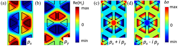
Figure F1. Out-of-plane magnetic field and in-plane electric field polarization in a cluster of six holes outlined by black triangles. (a) and (b) depict the real part of the out-of-plane magnetic field (Hz) for the eigenstates px and py respectively. The colors indicate the strength of Hz. (c) and (d) show , indicating the pseudo-spin nature of the bands excited at the Γ point with and modes, respectively.


Download figure:
Standard image High-resolution imageFrom this we find the relation

This implies that at the center of the clusters the in-plane electric field polarization is either - or -circularly polarized depending on the out-of-plane magnetic field eigenstates where . We can see this directly in figures F1 (c) and (d), which show where , characterizing the degree of circular polarization. In both cases we see that at the center the in-plane electric field is highly circularly polarized, except with opposite handedness. Thus the out-of-plane magnetic field eigenstates p± have an associated in-plane electric field circular polarization of which act as pseudo-spins for this topological photonic crystal.


Footnotes
- 6
For more details, see appendix.