


Abstract
Bifunctional effects of the Si atoms intercalated between the n-type 6H–SiC(0001) substrate and the  zero layer have been disclosed by scanning tunneling microscopy, low-energy electron diffraction, high-resolution synchrotron photoemission spectroscopy and angle-resolved photoemission spectroscopy. As a result of Si intercalation, an ordered Si interfacial layer composed of a Si adlayer and Si adatoms with dangling bonds has been formed under quasi-free-standing epitaxial graphene (EG). It turns out that the SiC(0001) band bending is determined by the Fermi level located close to the lowest states of the upper Hubbard band. The Hubbard bands originate from strong correlation effects of the electrons in the dangling bonds of the Si adatoms ordered on the Si adlayer. The doping level of the decoupled graphene is determined by the amount of charge transferred from the Si adatoms ordered on the Si adlayer to the quasi-free-standing EG.
Export citation and abstract BibTeX RIS

Content from this work may be used under the terms of the Creative Commons Attribution 3.0 licence. Any further distribution of this work must maintain attribution to the author(s) and the title of the work, journal citation and DOI.
1. Introduction
Graphene is a single sheet of graphite composed of two sublattices of sp2-hybridized C atoms in a honeycomb lattice. Its superior electronic and optical properties owing to the linear dispersion of the π and  bands (formed by the pz orbitals perpendicular to the plane of graphene) crossing at the Dirac point (ED) in the vicinity of the
  point of its hexagonal Brillouin zone make it extremely appealing for a wide range of applications [1]. Compared to other methods in fabricating graphene such as mechanical exfoliation, chemical exfoliation (via graphene oxide) and chemical vapor deposition on transition metals, large-area graphene epitaxy achieved by sublimation of Si from single-crystal SiC(0001) substrates provides a better possibility for integration in existing device technology suitable for high-frequency transistors and other electronic devices [2–5]. However, a high intrinsic electron doping (
 cm−2) and the degradation of the electrical properties such as a reduced electron mobility (
 cm2 V−1 s−1) compared to exfoliated graphene flakes, due to the influence of the
  reconstructed interfacial layer present between graphene and SiC(0001), limit the usage of such substrates [6–8]. This interfacial layer is constituted of C atoms arranged in a graphene-like honeycomb structure. About one third of these C atoms are covalently bonded with the top Si atoms of the SiC(0001) surface. Such partial sp3 hybridization of the interfacial layer prevents the formation of π bands and therefore the interfacial layer loses graphene-like properties [9]. Thus, such an electronically inactive interfacial layer is often called the buffer layer or the zero layer (ZL) [1, 7, 10]. However, the ZL plays an important role in passivating the dangling bonds of the SiC(0001) substrate, so that the overlying graphene layer exhibits truly delocalized π orbitals. An elegant way to remove the undesirable influence of the ZL on the overlying graphene is to prepare so-called quasi-free-standing epitaxial graphene (EG) through decoupling the ZL from the substrate [2] by the intercalation of various elements such as H [5, 10–17], Li [18], Na [19], O [20–22], F [2, 23], Au [9, 24], Cu [25], Fe [26, 27], Yb [28], Al [29], Pt [30], Ge [7, 31, 32] and Si [33–35]. Among them, semiconducting elements in group IV, like Si and Ge, turn out to be easily intercalated by deposition at room temperature (RT) and postannealing at elevated temperatures. As a result of such intercalation, the ZL is fully decoupled and the true graphene-like properties of the resulting decoupled ZL have been recovered. Even though Xia et al studied the Si intercalation on ZL and monolayer (ML) graphene on SiC(0001) using low-energy electron microscopy (LEEM), micro-low-energy electron diffraction (μ-LEED), high-resolution core-level and valence-band photoemission spectroscopy (PES) and angle-resolved photoemission spectroscopy (ARPES), their research was focused on ML graphene without understanding the detailed atomic structure of the interface [33]. Astonishingly, until now, the atomic structure of the interfacial layer after intercalation has not been studied using scanning tunneling microscopy (STM) except limited cases such as H [13, 14], F [2], Au [9, 24] and Cu [25].
In the present work, using STM, LEED, PES and ARPES, we have investigated on the intercalation effects originating from ordered Si atoms between the ZL and the n-type 6H–SiC(0001) substrate such as the doping of decoupled graphene as well as the substrate band bending. In our experiments, STM was employed to resolve the atomic structure of the intercalated Si interfacial layer. Both LEED and PES were used to confirm the decoupling of the ZL from the SiC(0001) substrate after Si deposition at RT and subsequent annealing. The π bands of quasi-free-standing monolayer graphene (QFMLG) were monitored directly by ARPES in the vicinity of the  point of its graphene Brillouin zone.
2. Experimental
A substrate with a size of 3 × 8 × 0.3 mm3 was cut from an on-axis n-type (N-doped) 6H–SiC(0001) wafer purchased from SiCrystal AG. It was transferred to an ultrahigh vacuum (UHV) chamber and outgassed for 12 h at 900 °C. Its native oxide-free surface was prepared through exposing the sample held at 900 °C to a Si flux [36]. The Si flux was generated by heating a slice of Si wafer at 1300 °C. After a further postannealing at 1150 °C for 5 min without Si, the  ZL was obtained in situ. Si atoms of an amount of 3.3 ML were deposited on this ZL at RT and postannealed at elevated temperatures. One ML is defined to be the ideal Si atom density on the SiC(0001) surface, i.e.,
  atoms cm−2 [31, 37]. The deposition amount was measured by a quartz crystal microbalance. The temperature was checked by an optical pyrometer at an emissivity of 0.90. All of the topographic STM images, the LEED patterns, the band structures around the
  point and the core-level/valence-band spectra were acquired at RT. The STM images were obtained using an RHK UHV 300 controlled by an RHK SPM 100 in constant current mode (tunneling current: 0.5 nA) with electrochemically etched W tips under UHV of 1 × 10⁻¹⁰ Torr and processed with imaging software, WSxM [38]. Along with monitoring the surface structures with the LEED patterns, the high-resolution ARPES data were obtained in the vicinity of the
  point by 34 eV photons at the 4A2 undulator beam line of the Pohang Accelerator Laboratory (PAL) in Korea using a VG Scienta R4000 analyzer. The overall energy and angular resolutions were 0.02 eV and
  , respectively. Both core-level and valence-band photoemission spectra were obtained at normal emission geometry at the 8A2 undulator beam line of the PAL using a high-resolution electron analyzer, Scienta SES 100. The valence-band spectra were obtained by 132 eV photons, while the C 1s (Si 2p) core-level spectra were obtained by bulk-sensitive 520 eV (326 eV) photons and surface-sensitive 326 eV (132 eV) photons.
After subtracting the Shirley-type background, the C 1s and Si 2p core-level spectra were analyzed by a standard least-squares fitting procedure generally using Voigt functions. Specially, for the graphene-related C 1s component, a Doniach-Šunjić profile was used to account for its conducting behaviour [10].
3. Results and discussion
3.1. Evidence of the ordered Si layer intercalated between QFMLG and SiC(0001)
As shown in figures 1(a) and (b), both STM and LEED images obtained from the surface prepared by postannealing the oxide-removed 6H–SiC(0001) sample at 1150 °C for 5 min displays a well-known image and pattern of the  ZL [39–41]. In this STM image, the solid (dotted) rhombus represents a unit cell of
  (6×6). The LEED pattern contains brightest spots of the SiC substrate (S) and bright spots of the graphene-like ZL (G) together with dim superstructure spots surrounding the S and G spots [42]. The ARPES spectrum obtained from this surface does not show any graphene-like π bands, as seen in figure 1(c). Instead, only two localized states, g1 and g2, appear at binding energies near 0.5 and 1.5 eV, respectively [43]. These results say that the surface is covered with the ZL without any ML graphene.
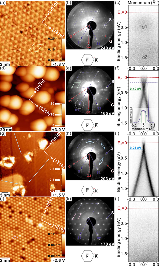
Figure 1. STM images at It = 0.5 nA (left panel), LEED patterns (middle panel) and band structures around the  point of the graphene Brillouin zone measured by ARPES (right panel) in the steps of the Si intercalation between the ZL and the SiC(0001) substrate. (a)–(c) Before Si deposition from the clean ZL. After 3.3 ML Si deposition at RT and postannealing for 5 min at (d)–(f) 650 °C, (g)–(i) 750 °C and (j)–(l) 850 °C. The reciprocal lattice vectors of the SiC (S1, S2) and graphene (G1, G2) lattices are indicated. In (b), (e), (h) and (k), dotted rhombuses represent unit cells of SiC(0001)-1 × 1; in (e), (h) and (k), solid rhombuses represent unit cells of 3 × 3,
  and 3 × 3, respectively. On the lower part of (f), a momentum distribution curve following the blue dashed line is shown.
Download figure:
Standard image High-resolution imageAfter 3.3 ML Si deposition on this ZL at RT and subsequent annealing at 650 °C for 5 min, the obtained STM image shows large and round clusters covering most of the surface, as shown in figure 1(d). The corresponding LEED pattern shows weak 3 × 3 spots whose unit cell is outlined by a solid rhombus and dim  spots inside the white circle, as shown in figure 1(e). As shown in figure 1(f), in the vicinity of the
  point, a pair of π bands appear; one having a charge neutrality point (ED) at 0.42 eV below the Fermi level (EF) and the other with a weaker ED difficult to appoint its position exactly. This is supported by a momentum distribution curve at a binding energy of 0.16 eV on the lower part of figure 1(f) [44]. From the LEED pattern and the π bands, it can be concluded that the deposited Si atoms are partially intercalated and part of the ZL is decoupled from the substrate. Due to electron transfer from the intercalated Si layer, the decoupled graphene with a structure of 3 × 3 exhibits an electron doping of
  cm−2, since
  ), where
  is 0.42 eV, ℏ is the Planck constant divided by 2π and the Fermi velocity vF is
  m s−1 [45].
After an extended postannealing at 750 °C for 5 min, as shown in figure 1(g), the STM image shows only a one-dimensional (1D) structure with three directions equivalent to the ![$[10\bar{1}0]$](https://content.cld.iop.org/journals/1367-2630/17/8/083058/revision1/njp518183ieqn23.gif) direction together with scattered 0.5 nm high craters. In the corresponding LEED pattern, figure 1(h), the ZL-related spots disappeared totally and there appear dim rows of spots along the three equivalent directions (i.e., having an angle of
direction together with scattered 0.5 nm high craters. In the corresponding LEED pattern, figure 1(h), the ZL-related spots disappeared totally and there appear dim rows of spots along the three equivalent directions (i.e., having an angle of  between any two) as well as bright S and G spots. Such a LEED pattern except G spots was already depicted by Naitoh et al for a new kind of Si-rich structure on the SiC(0001) surface having neither graphene nor ZL [46]. In here, a unit cell is marked by a long rhombus. In the vicinity of the
  point, as shown in figure 1(i), only a single sharp π band appears as expected for pristine graphene. This means that through full intercalation of Si between the SiC(0001) substrate and the ZL, the ZL becomes QFMLG. Therefore, it can be deduced that the 1D structure shown in figure 1(g) is reconstructed on the SiC(0001) substrate and imaged through this decoupled graphene. Since Si atoms cannot be intercalated through defect-free graphene, it can be concluded that they penetrate through the ZL by way of the observed craters, which appear as dark spots in the LEEM images reported by Xia et al [33]. When the amount of Si deposition at RT was less than 2 MLs, even after 750 °C annealing, Si atoms remaining on the ZL and do not intercalate, since the craters were not formed. It was also reported that Li atoms create defects/cracks on the graphene layer and penetrate through those defects to the ZL [18]. This decoupled graphene shows a ED at 0.21 eV below the EF in figure 1(i), which appeared already as the faint π band in figure 1(f). This decoupled graphene exhibits a much-reduced electron doping of
  cm−2, which implies that the 1D structure shown in figure 1(g) is well ordered and passivates the substrate more effectively than the ZL or the Si-intercalated 3 × 3 structure shown at 650 °C annealing. This decoupled graphene having ED = 0.21 eV survives even at 800 °C annealing.
However, after postannealing at 850 °C, as shown in figures 1(j) and (k), the surface is covered with the well-known three-layer 3 × 3 structure (as designated by solid rhombuses) which appears on the Si-rich SiC(0001) surface [47]. Its accepted model composed of a Si adlayer (bound to the top Si atoms of the substrate), Si trimers and Si adatoms was proposed by Starke et al through density functional theory analysis on STM and LEED results [48]. The band structure around the  point shows neither decoupled graphene-related π band nor ZL-related localized states, g1 and g2. This implies that the decoupled graphene is destroyed as a result of formation of SiC layers through reaction between C atoms of the decoupled graphene and Si atoms provided from either the intercalated Si layer or the craters, while extra Si atoms form the three-layer 3 × 3 structure at this temperature.
Additional annealing at 1000 °C induced the well-known  structure composed of Si adatoms on the clean bulk-terminated SiC(0001) surface. Finally postannealing at 1150 °C for 5 min gave rise to the recovery of the ZL (not shown here) [36, 49].
3.2. Evolving interfacial reconstruction of the intercalated Si atoms
In figure 2, the STM images of the intercalated Si atoms between the decoupled graphene and the SiC(0001) substrate are shown. Magnified images, figures 2(a) and (b), obtained from the same area in a terrace of the 650 °C annealed surfaces shown in figure 1(d) are characterized by a 3 × 3 structure whose unit cell is marked by solid rhombuses. As expected from the faint LEED pattern in figure 1(e) and the strong doping estimated from figure 1(f), the surface is not so well-ordered and there exist a lot of defects such as dark dips; especially, the filled-state STM image of figure 2(b) shows a lot of disorder. Even though this 3 × 3 structure is thought to be composed of a Si adlayer and Si adatoms, it is different from the one in figure 1(j), which emerges in the Si-rich SiC(0001) surface (without any graphene layer) composed of an adlayer, three trimers and an adatom having a dangling bond per 3 × 3 unit cell [47, 48]. In figure 2(c) shown is the image of the decoupled 1 × 1 graphene layer on the 3 × 3 Si interfacial layer, which was obtained by a tip different from that used in obtaining figures 2(a) and (b), probably a C-end tip. A graphene 1 × 1 unit cell marked by a small rhombus (lattice constant: 0.246 nm) is rotated by  relative to the 3 × 3 structure designated by a large rhombus.

Figure 2. Empty-state (positive bias voltage) and filled-state (negative bias voltage) STM images obtained from the ordered Si atoms intercalated between the ZL and the SiC(0001) substrate (It = 0.5 nA). 3.3 ML Si deposition at RT and subsequent annealing for 5 min at (a)–(c) 650 °C, (d)–(f) 750 °C and (g)–(i) 800 °C. In (a) and (b), (d) and (e) and (g)–(i), the intercalated Si structures are imaged through transparent QFMLG. In (c) and (f), the QFMLG structures are shown. Reconstructions of Si layers, (a) and (b) 3 × 3, (d) and (e)  , (g) transition from
  to
to  and (h) and (i)
  are shown. On the lower parts of (d) and (e), and on the upper parts of (h) and (i) shown are the corresponding top- and side-view models on the ordered Si atoms on SiC(0001) without graphene, which were proposed by Naitoh et al. Adapted with permission from [46]. Copyright 1999, AIP Publishing LLC.
Download figure:
Standard image High-resolution imageIn figures 2(d) and (e) shown are an empty- and a filled-state STM images obtained from the same area of the 750 °C annealed surface. They correspond to magnified images of the 1D structure already shown in the terrace of figure 1(g). Such a 1D structure, composed of narrow two-protrusion rows and broad four-protrusion rows along the [ ] direction, was also reported from on Si-rich SiC(0001) having neither graphene nor ZL [37, 46, 50]. Considering the symmetry of this structure, a conventional (primitive) unit cell is drawn by a solid rectangle (dotted rhombus) on the upper part in figure 2(e). In here, a thick solid (dashed) line represents an axis of reflection (glide reflection). So this 1D symmetry belongs to plane group cm [51]. For simplicity, from now on, this structure will be named as
  (lattice constants: 4.31 nm × 1.07 nm) referring from the conventional unit cell's length and width relative to the lattice constant of SiC(0001)-1 × 1, 0.308 nm. Naitoh et al, who also observed the identical structure from Si-rich SiC(0001), proposed a two-layer model composed of an adlayer with two holes (twenty-six atoms) and eight adatoms per primitive unit cell for this 1D structure by removing the third layer of the 3 × 3 structure and rearranging the first and the second layers [46]. This model is depicted on the STM images of figures 2(d) and (e). The side-view model is also drawn at the bottom of figure 2(d). The brightness asymmetry to the [
 ] direction in the filled-state STM image in figure 2(e) can be explained by two types of Si adatom sites depending on existence of underlying C atoms [46]. The Si coverage of the corresponding model, 34/28(=1.214) ML, is less than that of the three-layer 3 × 3 structure, 13/9(=1.444) ML [48]. The annealing period was increased long enough at 750 °C, but the intercalated Si structure remained as
  . Even though the dangling bond density is increased from 1/9(=0.111) ML of the three-layer 3 × 3 structure to 10/28(=0.357) ML of the
  structure, the interaction with the decoupled graphene prevents the SiC(0001) surface from forming the three-layer 3 × 3 structure under the graphene, since the
  structure is the most stable under the present condition. In figure 2(f) shown is the image of the decoupled graphene on the
  structure at a low bias voltage of
  eV. At the same time, the
  structure appears vaguely, whose primitive unit cell is marked by a long dotted rhombus. The graphene superstructure appears to be
  , instead of 1 × 1, as marked by a small rhombus (0.427 nm × 0.427 nm) in figure 2(f). Such a reconstruction of the decoupled graphene is known to be due to quantum interferences generated by static impurities at low bias voltages [52, 53].
With postannealing the sample at 800 °C, as shown in figure 2(g), broad four-protrusion rows almost disappear and narrow two-protrusion rows become dominant. In figure 2(h) and (i) shown are the detailed images of the area having only two-protrusion rows. The corresponding atomic structural model, constructed through removing the four-adatom rows and rearranging two-adatom rows of Naitoh et al's  model, is overlapped with the image. The corresponding side-view model is also shown above the top-view model in figure 2(i). As marked by the dotted rectangle in figures 2(h) and (i) (corresponding to a unit cell), such a structure belongs to plane group pg having only axes of glide reflection marked by dashed lines [51]. For simplicity, from now on, this structure will be named as
  (1.23 nm × 1.07 nm) referring from the unit cell's length and width relative to the lattice constant of SiC(0001)-1 × 1. The Si coverage of this model is 18/16(=1.125) ML, 7% less than that of the
  structure, 1.214 ML, meaning that a small amount of Si atoms has been deintercalated. The dangling bond density is also increased by 5% from 10/28(=0.357) ML of
  to 6/16(=0.375) ML.
3.3. Interfacial evolution in the process of Si intercalation
In figure 3, high-resolution synchrotron photoemission spectra of the C 1s core levels obtained in the steps of Si intercalation are shown. These spectra were obtained by bulk-sensitive 520 eV photons (left panel) and surface-sensitive 326 eV photons (right panel). The corresponding fitting parameters including binding energies (EBs), relative intensities (RIs) referred to that of component B of the ZL and Gaussian widths (GWs) are listed in table 1.

Figure 3. C 1s core-level photoemission spectra obtained by bulk-sensitive 520 eV photons (left panel) and surface-sensitive 326 eV photons (right panel). (a) ZL on 6H–SiC(0001) before Si deposition. After 3.3 ML Si deposition at (b) RT and postannealing for 5 min at (c) 650 °C, (d) 750 °C, (e) 850 °C and (f) 1150 °C. All of the spectra are normalized to the incoming photon flux and the curve fitting results are listed in table 1. In the right panel of (d), a side-view model is drawn in order to show the origins of components S2, S1, T, B, G,  and
and  .
.
Download figure:
Standard image High-resolution imageTable 1. Fitting results for binding energies (EBs) and Gaussian widths (GWs) of the C 1s spectra shown in figure 3 obtained by photon energies (EPhs) of 520 and 326 eV. Relative intensities (RIs) are referred to the photoemission intensity of component B of the ZL. Lorentzian width: 0.20 eV and asymmetry parameter of component G: 0.08.
| Spectrum | (a) ZL | (b) RT | (c) 650 °C | (d) 750 °C | (e) 850 °C | (f) 1150 °C | |||||||||||||
|---|---|---|---|---|---|---|---|---|---|---|---|---|---|---|---|---|---|---|---|
| component | EPh | EB | RI | GW | EB | RI | GW | EB | RI | GW | EB | RI | GW | EB | RI | GW | EB | RI | GW |
| (eV) | (eV) | (eV) | (eV) | (eV) | (eV) | (eV) | (eV) | (eV) | (eV) | (eV) | (eV) | (eV) | |||||||
| B | 520 | 283.73 | 1.00 | 0.63 | 283.60 | 0.38 | 0.63 | 283.85 | 0.28 | 0.56 | 283.89 | 0.07 | 0.52 | 283.80 | 0.08 | 0.62 | 283.70 | 1.00 | 0.66 |
| 326 | 283.73 | 1.00 | 0.63 | 283.64 | 0.15 | 0.63 | 283.83 | 0.29 | 0.56 | 283.92 | 0.11 | 0.52 | 283.80 | 0.06 | 0.62 | 283.70 | 0.83 | 0.66 | |
B
|
520 | 282.88 | 0.31 | 0.56 | 282.83 | 0.56 | 0.52 | 282.98 | 1.05 | 0.62 | |||||||||
| 326 | 282.79 | 0.21 | 0.56 | 282.76 | 0.36 | 0.52 | 282.81 | 0.85 | 0.62 | ||||||||||
| T | 520 | 284.15 | 0.20 | 0.63 | 284.02 | 0.08 | 0.63 | 284.27 | 0.06 | 0.56 | 284.31 | 0.01 | 0.52 | 284.22 | 0.02 | 0.62 | 284.20 | 0.33 | 0.66 |
| 326 | 284.15 | 0.48 | 0.63 | 284.08 | 0.04 | 0.63 | 284.36 | 0.03 | 0.56 | 284.34 | 0.01 | 0.52 | 284.22 | 0.02 | 0.62 | 284.16 | 0.77 | 0.66 | |
T
|
520 | 283.46 | 0.17 | 0.56 | 283.23 | 0.14 | 0.52 | 283.37 | 0.24 | 0.62 | |||||||||
| 326 | 283.37 | 0.11 | 0.56 | 283.16 | 0.10 | 0.52 | 283.20 | 0.35 | 0.62 | ||||||||||
| S1 | 520 | 284.89 | 0.94 | 0.80 | 284.79 | 0.55 | 0.62 | 284.98 | 0.61 | 0.69 | 284.87 | 0.35 | 0.44 | 284.85 | 0.24 | 0.76 | 285.06 | 0.78 | 0.82 |
| 326 | 284.82 | 3.17 | 0.71 | 284.75 | 0.97 | 0.60 | 284.97 | 2.10 | 0.69 | 284.96 | 0.42 | 0.61 | 284.88 | 0.73 | 0.76 | 285.00 | 2.77 | 0.74 | |
| S2 | 520 | 285.67 | 1.56 | 0.83 | 285.51 | 0.41 | 0.87 | 285.72 | 0.48 | 0.69 | 285.63 | 0.11 | 0.69 | 285.72 | 0.09 | 0.72 | 285.73 | 1.53 | 0.82 |
| 326 | 285.59 | 5.30 | 0.93 | 285.56 | 0.81 | 0.86 | 285.72 | 1.21 | 0.69 | 285.70 | 0.26 | 0.69 | 285.69 | 0.24 | 0.76 | 285.70 | 5.26 | 0.88 | |
| G | 520 | 284.72 | 0.97 | 0.34 | 284.67 | 1.81 | 0.31 | 284.74 | 0.30 | 0.35 | |||||||||
| 326 | 284.70 | 3.81 | 0.32 | 284.67 | 8.36 | 0.30 | 284.74 | 1.13 | 0.34 | ||||||||||
In figure 3(a), the spectra of the ZL before Si deposition are decomposed to four components. One bulk-related component B at EB = 283.73 eV and two ZL-related components, S1 at EB = 284.89 eV and S2 at EB = 285.67 eV, are identified. Component S1 originates from the ZL C atoms bonding to the underlying top Si atoms of the SiC substrate, while component S2 originates from the remaining ZL C atoms [43]. From the ratio, RI(S1)/[RI(S1) + RI(S2)] = 0.38, it can be deduced that 38% of the C atoms of the ZL belong to component S1. The fourth component T at EB = 284.15 eV was introduced for consistent EB(s) of the other components at EPhs of both 510 and 326 eV. This is assigned to the top C atoms of the SiC bulk, since it [RI(326 eV)/RI(520 eV) = 2.4] is more surface-sensitive than component B [RI(326 eV)/RI(520 eV) = 1] and less surface-sensitive than components S1 and S2 [RI(326 eV)/RI(520 eV) = 3.4].
After 3.3 ML Si deposition at RT, the C 1s spectra have the same B, S1, S2 and T components, as shown in the twice-expanded spectra of figure 3(b). Their RIs are quite reduced owing to the thick Si overlayer on the ZL. One distinct difference between before and after Si deposition is in the ratio of the RIs, RI(S1)/[RI(S1)+RI(S2)], which changes from 0.38 to 0.55. In other words, 17% of the C atoms in the ZL are additionally bonded with deposited Si atoms, since some of the C atoms of the ZL are chemically active differently from pristine graphene. These Si atoms bonding with the C atoms of the ZL make craters for Si atoms to penetrate. It has been reported that the existence of an sp2-to-sp3 rehybridization originating from the up- and down-relaxation in the ZL is associated with enhancement of the chemical reactivity of the ZL C atoms [54–57]. The buckled-up sp3-like C atoms with upward dangling bonds, estimated at least to be 17% of the ZL's C atoms, can be the origin of strong bonding to deposited Si atoms. So, Si atoms in the intercalated area move to the non-intercalated area, when postannealing the sample at 650 °C, since the decoupled graphene is inert.
After 650 °C postannealing, as shown in figure 3(c), three additional components  ,
,  and G appear along with the original components B, T, S1 and S2 as a result of partial intercalation. Surface-sensitive component G [RI(326 eV)/RI(520 eV) = 4.0] at EB = 284.72 eV with asymmetry can be assigned to the conductive graphene decoupled by Si intercalation and bulk-sensitive components
  [RI(326 eV)/RI(520 eV) = 0.68] at EB = 282.88 eV and
  [RI(326 eV)/RI(520 eV) = 0.65] at EB = 283.46 eV are assigned, respectively, to the bulk C atoms of the SiC substrate and to the top C atoms of the SiC substrate under the intercalated Si 3 × 3 layer shown in figures 1(d)–(f) and figures 2(a)–(c). Component
  (EB = 282.88 eV) has a lower binding energy by 0.85 eV than component B (EB = 283.73 eV) of figure 3(a), which implies that the intercalated Si 3 × 3 layer induces 0.85 eV more band bending than that of the ZL.
After 750 °C postannealing, as shown in figure 3(d), the RIs of components B, T, S1 and S2 originating from non-intercalated ZL area decreased, while the RIs of components  ,
,  and G increased. Since the corresponding STM images shown in figure 1(g) and figures 2(d)–(f) indicate the Si intercalation on the terrace, such components related to the remaining ZL area shown in figure 3(d) must be due to some of defective areas like craters and steps, where Si intercalation is blocked. The RI of component G at 750 °C annealing (1.81 at EPh = 520 eV and 8.36 at EPh = 326 eV) becomes about twice that at 650 °C annealing (0.97 at EPh = 520 eV and 3.81 at EPh = 326 eV). The RI of component
  also increases by 81% (i.e., from 0.31 to 0.56 at EPh = 520 eV). These mean that, at 650 °C annealing, the intercalated area is about half the total surface. The binding energy difference between component
  (EB = 282.83 eV) and component B (EB = 283.73 eV) of figure 3(a) indicates that the intercalated Si
  layer induces 0.90 eV more band bending than that of the clean ZL. When increasing the postannealing temperature from 650 °C to 750 °C, even though the ED moves by 0.21 eV as shown in figures 1(f) and (i), the EB of component G shows almost no change. This fact indicates that the doping level movement of the decoupled graphene is not directly related to the Fermi level movement of the substrate.
After 850 °C annealing, as shown in figure 3(e), the RI of component G decreases to 15%, while the RI of component  becomes twice, since most of the decoupled graphene was destroyed by the reaction with Si, forming the three-layer 3 × 3 structure on SiC layers, as shown in figure 1(j). The remaining graphene exists as small flakes, which can be rotationally disordered on the three-layer 3 × 3 structure, as on the SiC(
 ) surface [43, 58]. As a result, π band crossing around the
  point does not appear in figure 1(l). The EB of component
  , 282.98 eV, is similar to that a previously reported result, 283.05 eV for the three-layer 3 × 3 structure [49]. This structure shows 0.75 eV more band bending (i.e., 283.73–282.98 eV) than that of the clean ZL in figure 3(a).
After 1150 °C annealing for 5 min, as shown in figure 3(f), the ZL has been recovered. The ratio of component S2's RI to component S1's RI approaches to 2 [43]. Since the SiC(0001)-1 × 1 unit vectors are 0.308 nm long and the graphene 1 × 1 unit vectors are 0.246 nm long, a  cell contains 108 Si atoms on the top layer and a commensurate 13 × 13 graphene cells have 338 C atoms (two C atoms per unit cell) [41]. So, 108 C atoms can be bonded to the Si atoms on the top layer and the other 230 C atoms remain unbound; thus their ratio is close to 1:2. Both processes, Si intercalation and graphene destruction, induce larger ZL terraces with less contamination or defects, since the ZL or graphene acts as a barrier to the release of impurities from the surface and to the removal of the defect-related Si and C atoms.
In figure 4 shown are high-resolution synchrotron photoemission spectra of Si 2p obtained in parallel with C 1s shown in figure 3. The spectra were obtained using both bulk-sensitive 326 eV photons (left panel) and surface-sensitive 132 eV photons (right panel). Their fitting results are listed in table 2.
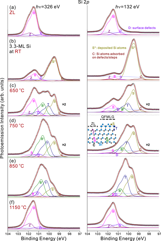
Figure 4. Si 2p core-level photoemission spectra obtained by bulk-sensitive 326 eV photons (left panel) and surface-sensitive 132 eV photons (right panel). (a) ZL on 6H–SiC(0001) before Si deposition. After 3.3 ML Si deposition at (b) RT and postannealing for 5 min at (c) 650 °C, (d) 750 °C, (e) 850 °C and (f) 1150 °C. All of the spectra are normalized to the incoming photon flux and the curve fitting results are listed in table 2. In the right panel of (d), a side-view model is drawn in order to show the origins of components B, Z,  , T and S.
Download figure:
Standard image High-resolution imageTable 2. Fitting results for binding energies (EBs) and Gaussian widths (GWs) of the Si 2p spectra shown in figure 4 obtained by photon energies (EPhs) of 326 and 132 eV. Relative intensities (RIs) are referred to the photoemission intensity of component B of the ZL. Lorentzian width: 0.10 eV, spin–orbit splitting energy: 0.60 eV and branching ratio: 0.5.
| Spectrum | (a) ZL | (b) RT | (c) 650 °C | (d) 750 °C | (e) 850 °C | (f) 1150 °C | |||||||||||||
|---|---|---|---|---|---|---|---|---|---|---|---|---|---|---|---|---|---|---|---|
| component | EPh | EB | RI | GW | EB | RI | GW | EB | RI | GW | EB | RI | GW | EB | RI | GW | EB | RI | GW |
| (eV) | (eV) | (eV) | (eV) | (eV) | (eV) | (eV) | (eV) | (eV) | (eV) | (eV) | (eV) | (eV) | |||||||
| B | 326 | 101.44 | 1.00 | 0.60 | 101.33 | 0.29 | 0.60 | 101.46 | 0.34 | 0.60 | 101.54 | 0.05 | 0.60 | 101.49 | 0.06 | 0.60 | 101.44 | 0.91 | 0.60 |
| 132 | 101.43 | 1.00 | 0.60 | 101.30 | 0.11 | 0.60 | 101.45 | 0.18 | 0.60 | 101.50 | 0.03 | 0.60 | 101.48 | 0.03 | 0.60 | 101.44 | 0.93 | 0.60 | |
B
|
326 | 100.56 | 0.26 | 0.60 | 100.58 | 0.42 | 0.60 | 100.72 | 0.68 | 0.60 | |||||||||
| 132 | 100.54 | 0.12 | 0.60 | 100.58 | 0.16 | 0.60 | 100.84 | 0.39 | 0.60 | ||||||||||
| D | 326 | 100.74 | 0.07 | 0.60 | 100.80 | 0.07 | 0.60 | 101.02 | 0.19 | 0.60 | 100.97 | 0.06 | 0.60 | 101.09 | 0.21 | 0.60 | 100.83 | 0.09 | 0.60 |
| 132 | 100.79 | 0.14 | 0.60 | 100.75 | 0.04 | 0.60 | 101.00 | 0.03 | 0.60 | 101.17 | 0.01 | 0.60 | 101.18 | 0.04 | 0.60 | 100.82 | 0.20 | 0.60 | |
| Z | 326 | 101.80 | 0.13 | 0.60 | 101.69 | 0.06 | 0.60 | 101.81 | 0.04 | 0.60 | 101.83 | 0.22 | 0.60 | ||||||
| 132 | 101.81 | 0.12 | 0.60 | 101.67 | 0.04 | 0.60 | 101.78 | 0.03 | 0.60 | 101.86 | 0.16 | 0.60 | |||||||
| T | 326 | 100.03 | 0.20 | 0.60 | 100.13 | 0.32 | 0.60 | 100.25 | 0.65 | 0.60 | |||||||||
| 132 | 100.04 | 0.22 | 0.60 | 100.13 | 0.31 | 0.60 | 100.28 | 1.08 | 0.60 | ||||||||||
S |
326 | 99.43 | 0.96 | 0.68 | |||||||||||||||
| 132 | 99.42 | 2.04 | 0.73 | ||||||||||||||||
| S | 326 | 99.46 | 0.29 | 0.49 | 99.44 | 0.32 | 0.60 | 99.61 | 0.37 | 0.60 | |||||||||
| 132 | 99.48 | 0.55 | 0.59 | 99.47 | 0.55 | 0.60 | 99.63 | 1.08 | 0.60 | ||||||||||
| C | 326 | 98.67 | 0.01 | 0.24 | 98.86 | 0.02 | 0.60 | 98.72 | 0.02 | 0.60 | 99.02 | 0.04 | 0.60 | ||||||
| 132 | 98.78 | 0.07 | 0.45 | 98.79 | 0.06 | 0.54 | 98.81 | 0.08 | 0.60 | 99.00 | 0.12 | 0.60 | |||||||
In figure 4(a), the spectra of the ZL before Si deposition are decomposed to a SiC bulk-related component, B, at EB = 101.44 eV (similar to a previously reported result, 101.45 eV [49]), and two additional components, Z at EB = 101.80 eV and D at EB = 100.74 eV at a EPh of 326 eV. Component Z arises from the substrate Si atoms bonded to the C atoms of the ZL and component D is attributed to Si-terminated defect areas, which is not transformed to ZL [10]. After 3.3 ML Si deposition at RT, component S* originating from deposited Si atoms is detected and the RIs of components B and Z are attenuated by deposited Si atoms, as shown in figure 4(b). A weak surface-sensitive component C probably due to Si atoms adsorbed to defects/steps is detected additionally at the lowest EB.
In the Si 2p spectra of figure 4(c) obtained after 650 °C annealing, components  , T and S have been added to components B, Z, D and C. Component
  , originating from the SiC bulk under the decoupled graphene, is bulk-sensitive [RI(132 eV)/RI(326 eV) = 0.46]. Less bulk-sensitive component T [RI(132 eV)/RI(326 eV) = 1.1] is assigned to both the Si adlayer and the substrate Si atoms bonded to the Si adlayer. Surface-sensitive component S [RI(132 eV)/RI(326 eV) = 1.9], which has almost the same EB as component S*, is assigned to both the adatoms with dangling bonds in the intercalated Si atoms and still-not-intercalated Si atoms on the ZL. The band bending, estimated from the binding energy difference between component B of the ZL in figure 4(a) and component
  of the 650 °C annealed surface in figure 4(c), is 0.88 eV, which turns out to match well with that (0.85 eV) estimated in figures 3(a) and (c).
From the 750 °C annealed surface, as shown in figure 4(d), the same components as those in figure 4(c) except component Z are detected. The depletion of component Z implies that the whole ZL is decoupled from the SiC substrate by the intercalated Si  layer. The survival of components B and D is due to the remaining ZL area such as the craters and steps shown in figure 1(g), where Si intercalation is blocked. The band bending estimated from the binding energy difference between component B in figure 4(a) and component
  of the 750 °C annealed surface in figure 4(d) is 0.86 eV, which is similar to that (0.90 eV) estimated in figures 3(a) and (d). This band bending related to the appearance of components T and S of the intercalated Si
  layer is not so much different from that of the intercalated Si 3 × 3 layer.
After 850 °C annealing, as shown in figure 4(e), the RIs of components  , T and S have become much stronger than those of figure 4(d). Their enhancements originate from the destruction of the decoupled graphene. The EB of component
  , 100.72 eV, is the same as the previously reported result, 100.72 eV for the three-layer 3 × 3 structure [49]. This shows a band bending of 0.72 eV (i.e., 101.44–100.72 eV) compared to the clean ZL in figure 4(a), which is close to that (0.75 eV) estimated in figures 3(a) and (e). After 1150 °C annealing for 5 min, as shown in figure 4(f), the ZL has been recovered.
The valence band spectra obtained at normal emission during Si-intercalation process are shown in figure 5. Each valence band maximum at the surface (EVBM) marked by a vertical line is estimated by the difference [ ] between
  (the EB of C 1s component B in the cases of (a) ZL, (b) RT, (c) 650 °C and (f) 1150 °C or C 1s component
  in the cases of (c) 650 °C, (d) 750 °C and (e) 850 °C, listed in table 1 at EPh = 520 eV) and
  281.0 eV, which is the energy difference between the C 1s core level and the valence band maximum of bulk SiC, reported earlier) [49]. For example, the EVBM of spectrum 'd' is estimated by
  eV
eV 
 eV below EF. Spectrum 'a' of the ZL before 3.3 ML Si deposition is in good agreement with the previous reports on the
  ZL [59]. Two ZL-related localized states existing close to EF are marked by g1 and g2 [43]. Features between 2 and 12 eV originate from hybridization of C 2p and Si 3s + 3p states [33]. The 3.3 ML Si deposition at RT reduces the overall ZL-related states but the Si-cluster-related states around 2 eV increases, as shown in spectrum 'b'. Spectrum 'c' obtained after 650 °C annealing has features of both spectrum 'b' and spectrum 'd' due to partial intercalation. So it has two EVBMs. Postannealing the sample at 750 °C gives spectrum 'd' with features around EB = 0.7, 2–12 and 21 eV. The peak around 0.7 eV marked by L1 is related to the surface states caused by residual dangling bonds of the Si
  structure. A relatively strong feature around 3 eV is related to the Si 3s + 3p states of the Si
  interfacial layer, which is also seen in spectrum 'e'. A swollen area around 8 eV and a broad peak around 21 eV originate from a π band and a σ band of the decoupled graphene, respectively [5, 43]. Postannealing at 850 °C gives spectrum 'e' in good agreement with that of the three-layer Si 3 × 3 structure [49]. Spectra 'c', 'd' and 'e' say that all of the Si-rich structures on the SiC(0001) are semiconducting from nonexistence of surface states at EF2
. The semiconducting nature of the three-layer 3 × 3 structure arise from a Mott–Hubbard metal–insulator transition due to strong electron correlation effects of states localized at the Si adatom sites, leading to a filled lower Hubbard band and an unfilled upper Hubbard band inside the band gap [49, 60–62]. Since the
interfacial layer, which is also seen in spectrum 'e'. A swollen area around 8 eV and a broad peak around 21 eV originate from a π band and a σ band of the decoupled graphene, respectively [5, 43]. Postannealing at 850 °C gives spectrum 'e' in good agreement with that of the three-layer Si 3 × 3 structure [49]. Spectra 'c', 'd' and 'e' say that all of the Si-rich structures on the SiC(0001) are semiconducting from nonexistence of surface states at EF2
. The semiconducting nature of the three-layer 3 × 3 structure arise from a Mott–Hubbard metal–insulator transition due to strong electron correlation effects of states localized at the Si adatom sites, leading to a filled lower Hubbard band and an unfilled upper Hubbard band inside the band gap [49, 60–62]. Since the  structure also has adatoms as the three-layer 3 × 3 structure, the same kinds of Hubbard bands will be induced. In reality, spectra 'd' and 'e' are similar except graphene-related areas around EB = 8 and 21 eV. As a result, the
  layer is semiconducting and the lower Hubbard band L1 is formed inside the band gap as the three-layer 3 × 3, which can be seen in spectra 'd' and 'e' of figure 5. Postannealing this sample at 1150 °C for 5 min recovers the clean ZL having a broad density of states which extend up to EF, as shown in spectrum 'f '.

Figure 5. Valence band spectra obtained from n-type 6H–SiC(0001) with ZL during Si intercalation at normal emission. (a), (b) 6H–SiC(0001) with ZL before and after 3.3 ML Si deposition at RT. (c)–(f) After 650, 750, 850 and 1150 °C annealing, respectively. A dotted line and solid bars represent the Fermi level (EF) and the valence band maxima at the surface (EVBM), respectively. All of the spectra are normalized to the incoming photon flux.
Download figure:
Standard image High-resolution image3.4. Bifunctional effects of Si intercalation: SiC substrate band bending and graphene doping
The above-mentioned experimental results can be depicted by the band diagrams of the n-type 6H–SiC(0001) with the ZL and the  layer, as shown in figures 6(a) and (b), respectively. Figure 6(a) [6(b)] has been drawn using the 520 eV spectra of figure 3(f), figure 4(f) [figure 3(d), figure 4(d)], figure 5 and tables 1 and 2. In addition to these experimental results, referred are its band gap (Eg = 3.0 eV), its energy difference (281.0 eV) between the bulk C 1s core level and the valence band maximum (EVBM) and its theoretical bulk EF position, 2.9 eV above EVBM (i.e., 0.1 eV below the conduction band minimum (ECBM)), which were previously reported [49, 63].

Figure 6. Band diagrams of the n-type 6H–SiC(0001) with (a) the ZL and (b) the Si- interfacial layer covered with decoupled graphene. ⊖ represents polarization charge originating from the spontaneous polarization of the substrate (P). The sum of negative charge in the decoupled graphene and the polarization charge is the same as the positive charge of the upper Hubbard band, since the polarization is zero outside of the system. EF: Fermi level, ECBM: conduction band minimum, EVBM: valence band maximum, ED: Dirac point and Eg: band gap energy. g1: lower ZL state, g1
 : upper ZL state, D: C/Si dangling bond state, U1: upper Hubbard band and L1: lower Hubbard band. For letters and values lower than EVBM, the identical ones used in figures 3, 4 and 5 and tables 1 and 2 were employed.
Download figure:
Standard image High-resolution imageIn the diagram of the ZL in figure 6(a), since the EB of C 1s bulk component B is 283.70 eV, the surface EF is located at 2.7 eV above EVBM and the surface band bending (Schottky barrier) for the ZL turns out to be only 0.2 eV (0.3 eV). This surface EF is positioned near the upper limit of the g1 state located in the band gap, as shown in figure 1(c) and in spectra 'a' and 'f ' of figure 5. The filled (g1) and empty (g1 ) surface states are superimposed with band D associated with carbon (as well as silicon) dangling bonds and some defects extending up to the EF [36, 57, 59, 64]. If there existed ML graphene on this ZL, as the Dirac cone represented by dotted lines in figure 6(a), the graphene would show a very high electron doping level (ED = 0.42 eV below EF and
  cm−2) due to charge transfer from the ZL having high-density surface states [7, 10]. When the dangling bonds of the 6H–SiC(0001) surface is perfectly passivated by hydrogen intercalation and there is no surface state, the ML graphene exhibits a p-type conductivity with ED = 0.30 eV above EF and a hole density of
  cm−2 [11]. According to Ristein et al, this is due to the spontaneous polarization, P, of the substrate creating an acceptor layer, which is marked by minus signs in circles (⊖s), negative effective polarization charge, in figure 6 and the n-type doping of the ML graphene on the ZL was explained by donor-like states associated with the ZL which overcompensate this polarization doping [64]. If this is the case, the electron charge density provided by the ZL is estimated to be
  cm−2, which results in an electron doping of
  cm−2 to the decoupled graphene by compensating a hole density of
  cm−2due to spontaneous polarization.
In the diagram of the  layer in figure 6(b), since the EB of C 1s bulk component
  is 282.83 eV, the surface EF is located at 1.8 eV above EVBM and the surface band bending (Schottky barrier) for the ZL turns out to be only 1.1 eV (1.2 eV). Inside the band gap, the lower Hubbard band marked by L1 is filled with electrons and the normally empty upper Hubbard band marked by U1 is partially filled with electrons originating from the conduction band [49]. The surface EF is therefore fixed at a position close to the lowest states of band U1, inducing a band bending [36, 60, 61]. The electrons in band U1 in turn are transferred to the decoupled graphene and give n-type graphene doping of
  cm−2 corresponding to ED = 0.21 eV below EF. The electron charge density provided by the
  layer is estimated to be
  cm−2. When the intercalated Si layer structure is transformed into
  through postannealing at 800 °C as shown in figure 2(g), the EF and the ED show almost no difference from those of
  , since their basic structures are commonly composed of an adlayer and adatoms and even after full transformation the dangling bond density increases by only 5% from 10/28(=0.36) ML of
  to 6/16(=0.38) ML of
  in the models of figure 2. Since the dangling bond density of the
  layer is 0.36 ML per SiC(0001)-1 × 1 unit cell, under the assumptions that there exist essentially no unsaturated Si dangling bonds at the interface [43, 56] and that the electron charge density given to the ML graphene is proportional to the dangling bond density, the ZL has by itself about 0.75 dangling bond per SiC(0001)-1 × 1 unit cell [i.e., dangling bond density of
  {electron charge density provided by ZL}/{electron charge density provided by
  } = 0.36 ML
 cm−2/
cm−2/ cm−2]. Since the number of the ZL's C atoms per SiC(0001) unit cell is 338/108 (= 3.1), 0.75 ML is only 24% of the ZL's total C atoms. Even though, in section 3.3, it was mentioned that at least 17% C atoms of the ZL has dangling bonds, in reality more C atoms must have dangling bonds, since all of the C atoms with dangling bonds cannot bond to the deposited Si atoms due to dense C atoms in the ZL with a C–C bond-length of 0.142 nm. The intercalated 3 × 3 layer of the 650 °C annealed surface has almost the same EF position as the
  layer as shown figures 3(c) and 4(c), but its density of surface states is as high as that of the ZL, as shown in figure 1(f). This is due to the defect-related surface states, as shown figures 2(a) and (b).
4. Conclusions
The effects of the reconstructed Si atoms intercalated between the ZL and the SiC(0001) substrate on the doping of the decoupled graphene as well as the substrate band bending have been investigated by STM, LEED and (AR)PES. Some of deposited Si atoms chemically bond to the ZL at RT and induce craters, through which deposited Si atoms are intercalated between the ZL and the substrate by postannealing. With 650 °C annealing, the partially-intercalated Si atoms form a 3 × 3 layer with a lot of defects. With postannealing at higher temperatures between 750 and 800 °C, this layer transforms into the well-ordered Si layer of the  and
and  structures, which are composed of a Si adlayer and adatoms. Strong correlation among the electrons localized at these Si adatom sites induces Hubbard bands in the gap. The resulting Fermi level is positioned at 1.8 eV above the valence band maximum. As a result, the band is bent by about 0.9 eV compared to the surface with the non-intercalated ZL. While the decoupled graphene on the Si 3 × 3 layer with a lot of defects has an electron doping of
  cm−2, that on the Si-
 layer having a 1D structure exhibits a reduced electron doping of
  cm−2. This means that the Si-
 layer is more ordered and passivates the substrate more effectively. After 850 °C annealing, the decoupled graphene is destroyed by its chemical reaction with the Si atoms from the Si interfacial layer and the craters. However, with 1150 °C annealing, ZL is recovered.
From the present studies on the role of the interfacial layer, it can be concluded that the substrate band bending is determined by the relative location of the upper Hubbard band, originating from the correlation of electrons localized at adatoms of the ordered Si interfacial layer, inside the band gap of the substrate, while the doping of the QFMLG is determined by the efficiency of substrate passivation by the ordered Si interfacial layer, as well as the amount of charge transfer from the ordered Si interfacial layer to the decoupled graphene.
Acknowledgments
For conducting the present work, HK was supported by Nano-Material Technology Development Program through the National Research Foundation of Korea (NRF) funded by the Ministry of Science, ICT and Future Planning (No. 2012M3A7B4049888) and by Basic Science Research Program through the NRF funded by the Ministry of Education (No. NRF-2014R1A1A2055818). This work was also supported by the NRF grant funded by the Korean Government (MEST) (No. 2010–0022173).
Footnotes
- 2
Since the covering angle of the analyzer is not broad enough to reach the
 point, surface states at EF due to a conductive decoupled graphene layer do not appear in these spectra.
