


Abstract
Vertical oriented GaN microrods were grown by metal-organic vapor phase epitaxy with four different n-type carrier concentration sections above 1019 cm−3 along the c-axis. In cathodoluminescence investigations carried out on each section of the microrod, whispering gallery modes can be observed due to the hexagonal symmetry. Comparisons of the spectral positions of the modes from each section show the presence of an energy dependent mode shift, which suggest a carrier-induced refractive index change. The shift of the high energy edge of the near band edge emission points out that the band gap parameter in the analytical expression of the refractive index has to be modified. A proper adjustment of the band gap parameter explains the observed whispering gallery mode shift.
Export citation and abstract BibTeX RIS

Content from this work may be used under the terms of the Creative Commons Attribution 3.0 licence. Any further distribution of this work must maintain attribution to the author(s) and the title of the work, journal citation and DOI.
1. Introduction
The presence of whispering gallery modes (WGMs) with high quality (Q-)factors as well as lasing activity in GaN microrods enable their use as optical microcavities in applications such as polariton and photon lasers and ultrasensitive optical sensors [1–7]. Beside the size and shape of the microrods, the refractive index determines the optical properties of microcavities such as spectral positions of the WGMs. Therefore, it is important to know to identify processes, which influence the refractive index. The analysis of WGMs from microrod structures have already been used to determine the refractive index of GaN [8]. In such microrods, high carrier concentrations above 2 × 1020 cm−3 have been reported [9]. High carrier concentrations might modify the refractive index as it has been proposed in [10]. The current-induced refractive index change for carriers injected into a GaN based laser diode has already been reported [11]. In this letter, the influence of different high carrier concentrations on the refractive index of GaN will be investigated. GaN microrods were grown with four sections each having different doping concentrations. Cathodoluminescence (CL) measurements on each section show WGMs and a spectral energy dependent WGM shift as well as a shift of the near band edge (NBE) emission. The band gap parameter in the analytical expression of the refractive index can be modified to explain the WGM shift.
2. Experimental
The GaN microrod samples were grown by a self-catalyzed vapor-liquid-solid (VLS) method on 2 inch c-plane sapphire substrates utilizing an Aixtron 200RF horizontal flow metal-organic vapor phase epitaxy (MOVPE) reactor [12]. Trimethylgallium (TMGa), silane, hydrogen, and ammonia were used as precursors. Silane is needed for n-type doping and enhances the vertical growth due to the formation of surface SiN acting as a stabilization and antisurfactant layer [13]. The samples are grown at a pressure of 100 mbar and a susceptor temperature of 1150 °C. A V/III ratio of 6–25 was adjusted. All further details concerning growth can be found in [6, 12]. Scanning electron microscopy (SEM) and room temperature (RT) CL measurements were performed utilizing a Hitachi S4800 in combination with a Gatan MonoCL setup. For the SEM images and CL measurements an acceleration voltage of 5 keV and a sample tilt of 60° were used. Raman measurements were performed at RT in backscattering configuration using a LabRam HR800 spectrometer from Horiba Scientific. The linearly polarized laser emitting at 457 nm was focused by a 100 × objective (numerical aperture 0.9) resulting in a diameter of the normally incident probing beam of 0.7 μm and in a laser power on the sample surface of ∼582 μW using a filter.
3. Theoretical background
WGMs in a hexagonal structure are based on reflections of light either at six or three sidewall facets, designated as hexagonal or triangular WGMs, respectively [14]. In hexagonal cavities consisting of materials having a refractive index  (with n = 1 outside the cavity), triangular WGMs are dominant because Q-factors by up to two orders of magnitude higher compared to Q-factors from hexagonal WGMs are possible due to strong coupling of superscar modes [15]. Coupling of triangular WGMs results in a suppressed field distribution at the corners, thus reducing the scattering losses at the corners. Recalculations of the spectral positions of WGMs from microrods presented in a previous work [1] show much better agreement if triangular WGMs are used instead of hexagonal WGMs together with a multiplication of the refractive index by a fairly uncommon factor of 0.9103.
Spectral positions  of triangular WGMs, which are observed for the investigated microrod, can be calculated applying a simple plane wave model [14, 16]:

N is the mode number, β is  for transversal electric (TE) and
  for transversal magnetic (TM) polarization, respectively. The inner diameter di can be measured by SEM. The refractive index
  of GaN in the transparent region below the band gap can be determined from the real part of the dielectric function
  measured on strain free and undoped GaN by spectroscopic ellipsometry using
  [17, 18]. The experimental data of the ordinary and extraordinary refractive index are shown in figure 1. The following equation derived from the Kramers–Kronig relation can be used for analytical expression of the experimental data [19]:

The E0 parameter represents the effective band gap energy of GaN, A0 and A1 are magnitude parameters and E1 is the contribution of all high-energy optical transitions [19]. Using the parameters summarized in table 1, good agreement is achieved in a range between 1–3.37 eV for the ordinary and 1–3.36 eV for the extraordinary refractive index.
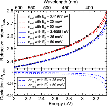
Figure 1. The upper plot shows the ordinary and extraordinary refractive index of GaN. The black symbols are experimental data taken from [17, 18]. Each solid line is a best fit using equation (2) together with the parameters in table 1. Each dashed and dotted line is calculated with a modified E0 parameter plus 25 and 50 meV, respectively. The lower plot shows the corresponding energy dependent deviation  (difference between the dashed/dotted and solid lines).
Download figure:
Standard image High-resolution imageTable 1. Best fit parameters for equation (2) of the experimental data shown in figure 1 for the ordinary and extraordinary refractive index of GaN, valid in a range between 1.00–3.37 eV and 1.00–3.36 eV, respectively.
| Refractive index | A0 | A1 (eV) | E0 (eV) | E1 (eV) |
|---|---|---|---|---|
| Ordinary | 1.52001 | 44.0405 | 3.40581 | 8.52205 |
| Extraordinary | 1.72242 | 43.4421 | 3.41977 | 8.08019 |
It has already been shown that the NBE emission peak position is dependent on the carrier concentration [20, 21]. A shift towards higher (lower) energy is expected for increasing carrier concentrations above (below) ∼8 × 1018 cm−3 due to the Burstein–Moss effect (band gap narrowing) [10, 20, 22, 23]. Therefore, it is necessary to check the influence of the band gap parameter E0 in the analytical expression of the refractive index. The ordinary and extraordinary refractive index has been calculated with a band gap parameter modified by +25 and +50 meV, respectively. It is shown in the upper graph of figure 1 that an increase of E0 slighlty decreases the refractive index. The lower graph in figure 1 displays the difference between the initial refractive index and the modified one. In the lower energy range there is only a small deviation. However, in the energy range close to the band gap there is a significant deviation of larger than 2%. Increasing E0 leads to a decreased differential change of the refractive index.
4. Results and discussion
4.1. Growth of GaN microrods with four different doping sections
A GaN microrod sample was grown with four sections of different doping concentrations along the c-axis. A sketch of the growth sequence is shown in figure 2. To initialize microrod growth, a high TMGa flow of 40 sccm (180 μmol min−1) is applied for 20 s. To improve the optical properties, TMGa was then reduced to a flow of 10 sccm within 50 s [6, 12, 24]. Afterwards, four microrod sections each with a growth time of 5 min and with different Si doping concentrations were deposited.

Figure 2. Growth scheme (left) and definition of the four sections of the microrod (right) with different Si doping concentrations. The basis of the microrod, grown with a higher TMGa flux, has different optical properties compared to the upper part and is therefore not considered in this study.
Download figure:
Standard image High-resolution image4.2. CL investigations of a single GaN microrod
Among an ensemble of differently sized microrods, a long GaN microrod is chosen for further investigations with a height and inner diameter of 9.21 ± 0.04 and 1.75 ± 0.01 μm, respectively. The diameter along the microrod axis is constant within the error range, i.e., no tapering such as in previous reported GaN wires is present [25] (for the details of the diameter measurements see the supplementary material). The SEM image of the microrod and the corresponding panchromatic CL image are shown in figures 3(a), (b). The basis grown with a high TMGa flux has poor optical properties (strong yellow defect luminescence and weak GaN NBE emission) and is not considered for the following investigations. Details on the optical properties can be found in [6]. The upper part of the microrod grown with a low TMGa flux having improved optical properties can be separated into four sections defined in figure 2: between each section there is a thin layer of different contrast visible in the panchromatic CL map in figure 3(b). From each section a CL spectra was recorded while fixing the focused electron beam at the center of each section (see figure 3(c)). Dominating NBE emission as well as weak yellow luminescence centered at 2.2 eV and surface related emission at 2.7 eV are visible [26].
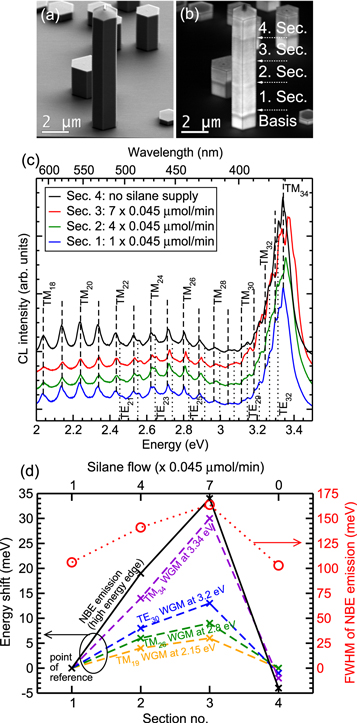
Figure 3. (a) shows an SEM image and (b) the corresponding panchromatic CL map of a microrod. The four sections of the microrod with different silane flows can be separated by the transitions with different CL contrast and are highlighted by the white dashed arrows. (c) CL spectra of the four sections each recorded with a fixed electron beam at the center of each section (shifted for clarity). The black dashed and dotted lines are calculated TM and TE triangular WGMs with mode numbers 18–34 and 21–32, respectively. (d) Graph shows the shift of the NBE emission and of four WGMs at different spectral positions (left axis). Furthermore, the FWHM of the NBE emission is plotted (right axis).
Download figure:
Standard image High-resolution image4.3. Observation of WGMs in each section of the microrod
Independent of the respective section of the microrod, WGMs are observed in the energy range from the NBE emission to the yellow defect luminescence. The spectral positions of the WGMs in the blue spectrum obtained from section 1 have been calculated using equation (1). The inner diameter used for the calculation was set to 1779.8 nm, which is in good agreement with the measured inner diameter of 1.75 ± 0.01 μm. The band gap parameter E0 was modified in order to get the best agreement between experimental and calculated data. For the ordinary and extraordinary refractive index, E0 was set to 3.386 and 3.429 eV to fit with the TE and TM WGMs, respectively. The calculated spectral positions of the WGMs are also in agreement with the black spectrum from section 4, but not in good agreement with the green and red spectra from sections 2 and 3, respectively, especially in the high energy range.
Figure 3(d) displays the energy shift of four selected WGMs at different energetical positions. There is a WGM shift towards higher energy with increasing silane flow and the shift is more pronounced at higher energies. The TM19 WGM at ∼2.15 eV shows only a small shift of up to 6 meV whereas the TM34 WGM at ∼3.34 eV is shifted by 30 meV with respect to the spectrum from section 1.
Due to the superposition of the NBE emission with WGMs, the NBE emission peak position can not unambiguously be determined. Compared to section 1, a NBE emission peak shift of ∼10 and ∼20 meV for sections 2 and 3, respectively, can roughly be estimated. However, these values are not very reliable due to the presence of WGMs at the peak and low energy edge of the NBE emission. A more precise estimation is possible when only considering the high energy edge of the NBE emission at half maximum which is not in superposition with WGMs. The shift is displayed in figure 3(d) (black line). With increasing the silane flow a shift up to 34 meV towards higher energy is observed, which can be explained by the Burstein–Moss effect.
4.4. Determination of the carrier-concentration by analysis of the FWHM of the GaN NBE emission
The FWHM of the NBE emission of each spectra was determined and is shown in figure 3(d) (right axis). Values in a range between 100–160 meV are present. The carrier concentration of each section was estimated from the FWHM of the NBE emission according to [27] and are summarized in table 2. High n-type carrier concentrations up to  cm−3 were found. The estimated carrier concentrations reveal that not all the supplied Si atoms are incorporated into GaN as dopants. An increase of silane supply by a factor of 4 and 7 enhances the carrier concentration only by a factor of ∼2 and ∼3, respectively. This is attributed to the self-catalytic VLS growth of the microrods and the low solubility of Si atoms into the Ga droplet on top of rod leading to enhanced formation of SiN on the sapphire surface and on the sidewalls of the rods acting as a sink for Si [12, 13, 28]. The high carrier concentrations above 1×1019 cm−3 in all four sections of the microrod are in agreement with the trend showing a shift of the high energy edge of the NBE emission towards higher energies [21].
Table 2. Summary of the carrier concentrations N obtained from FWHM of NBE emission (see figures 3(c), (d)) and from the LOPPCM-position in the Raman spectra (see figure 4). The LOPPCM-measured at 515 cm−1 corresponds to contributions from sections 1, 2 and 4.
| Silane flow |

|

|
LOPPCM- |

|
|
|---|---|---|---|---|---|
| Section | ( μmol min−1) μmol min−1) |
(meV) | (cm−3) | (cm−1) | (cm−3) |
| 1 | 1 | 106.0 |

|
∼515 | ∼5.4 × 10¹⁹ |
| 2 | 4 | 141.0 |

|
∼515 | ∼5.4 × 10¹⁹ |
| 3 | 7 | 163.7 |

|
528 | 2.7 × 10²⁰ |
| 4 | 0 | 102.9 |

|
∼515 | ∼5.4 × 10¹⁹ |
4.5. Determination of the carrier-concentration by analysis of the Raman spectra
Micro-Raman measurements were used as an additional method to determine the carrier concentration in the microrod [29, 30]. The micro-Raman spectra in figure 4 recorded on a single microrod show the A1(TO), E1(TO) and  (TO) modes at 531.3 , 558.2 and 567.2 cm−1, respectively. The values are comparable to Raman measurements on high-quality nonpolar and strain-free GaN substrates grown by hydride phase epitaxy [31]. The spectral position of the longitudinal optical phonon plasmon coupled mode (LOPPCM) provides information about the carrier concentration. A LOPPCM-and a LOPPCM+ peak show up below the transversal optical (TO) phonon frequency in the uncoupled mode
  (= 531.3 cm−1) and above the LO phonon frequency in the uncoupled mode
  (= 734 cm−1) for high and low carrier concentrations, respectively. The following equation, derived from the dielectric function, reproduces the N dependent LOPPCM ± frequency
  [32]:
[32]:

with the plasmon frequency  , e as the elementary charge,
  as the optical dielectric constant of GaN and
  as the effective mass of an electron in GaN valid for high doping concentrations [33].
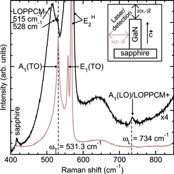
Figure 4. Micro-Raman spectra measured on a single microrod in top and side configurations shown in the inset. The dashed lines at  = 531.3 cm−1 and
  = 734 cm−1 indicate the positions of the TO and LO phonon frequency in the uncoupled mode, respectively.
Download figure:
Standard image High-resolution imageTwo measurement configurations have been used for the micro-Raman investigations as illustrated in the inset of figure 4 [34]. In the  configuration, i.e., laser excitation and detection is perpendicular to the microrod side-wall facet, the intense A1(TO) mode at ∼531.3 cm−1 covers the LOPPCM-peak. The latter is expected to be located between 500–531.4 cm−1 for high carrier concentrations above 3 × 1019 cm−3, as for the microrod in the present study. Therefore, each section of the microrod can not be analyzed by micro-Raman with respect to the LOPPCM-peak. The A1(TO) mode is not allowed in the
  configuration, i.e., laser excitation and detection is perpendicular to the microrod top facet, however, all sections are probed at once. Two LOPPCM-peaks are visible at 515 and 528 cm−1 corresponding to 5.4 × 10¹⁹ and
  cm−3, respectively, using equation (3). The LOPPCM-at 528 cm−1 originates from section 3 of the microrods, while the LOPPCM-at 515 cm−1 is a superposition of all other sections. The carrier concentrations obtained from micro-Raman measurements and from the FWHM of the NBE emission are in good agreement as can be seen in table 2. Finally, there is a peak at 735.5 cm−1 referred to a A1(LO)/LOPPCM+, which is expected to stem from unintentional doped GaN located at the base of the microrod formed during the initial microrod growth. Such a peak at 735.5 cm−1 (corresponds to a carrier concentration of 6 × 1016 cm−3 using equation (3)) can also be observed in unintentional doped GaN layers grown in the used MOVPE system (not shown here).
4.6. Adjusting the refractive index band gap parameter towards fitting of the spectral energy dependent WGM shift
Concerning the WGM shift, the NBE emission shift, and the FWHM, there is no significant difference between the spectra from sections 1 and 4, i.e., there is still some Si incorporation taking place after switching off silane supply during growth of section 4. High temperature decomposition of the surface SiN might act as a source leading to a background doping effect.
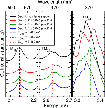
Figure 5 is showing a detailed view of three selected modes at different spectral positions with a small and large WGM shift at low and high energies, respectively, as already shown in figure 3(d). The blue dashed lines are the calculated  WGMs similar to figure 3(c). The new spectral positions of the WGMs for the green and red spectra obtained from sections 2 and 3, respectively, were also calculated. For that purpose, the band gap parameter E0 was set to 3.457 eV for the green spectra and to 3.480 eV for the red spectra, i.e., the initial E0 used for the blue spectra was modified by +28 and +51 meV. The trend of these values is in agreement with the high energy edge shift of the NBE emission. The green dashed–dotted and red dotted lines in figure 5 are in good agreement with the new spectral positions of the WGMs in the green and red spectra. The same modification of the ordinary refractive index is also in good agreement with the observed shift of the TE WGMs (not shown here).
Figure 5. Graph shows a detailed view of three WGMs TM19 (left graph), TM24 (center graph), and TM34 (right graph) from the four spectra obtained from each section of the microrod. The blue dashed, green dashed–dotted, and red dotted lines are calculated spectral positions of each WGM with  3.429 eV,
  3.458 eV, and
  3.480 eV, respectively.
Download figure:
Standard image High-resolution image
It was already stated that the diameter along the microrod is constant, however, a small variation of a few nm might not be measureable via SEM. Using equations (1) and (2) it can be calculated that a diameter reduction of 10 nm for the microrod having a diameter of 1780 nm would lead to a blue shift of 11, 13, 13 and 7 meV for the TM19, TM26, TM30, and TM34 WGM, respectively (for the details of the diameter dependent WGM shift see the supplementary material). Comparing these values with the observed WGM shift in figure 3(d), which shows an increasing WGM shift with increasing N, it is clear that a diameter variation can not be responsible for the observed WGM shift.
Si is known to induce tensile strain in a GaN layer leading to a reduction of the band gap [35–37]. This is in contrast with the data presented in figure 3(d) showing a blue shift with increasing the Si doping concentration and can therefore not be considered as a reason for the observed WGM shift.
It is clear that the carrier concentration effects the refractive index change, which leads to a WGM shift. The high carrier concentration induces a Burnstein–Moss shift, i.e., an increase of the band gap. A modification of the band gap parameter E0 in the refractive index equation (2) is therefore a proper tool to explain the WGM shift caused by different carrier concentrations.
The present study is not only limited to the GaN material system, but can also be applied to other material systems such as ZnO [38].
5. Conclusion
In conclusion, GaN microrods with four different doping concentration sections were grown by MOVPE. The carrier concentration in the range between 1019–1020 cm−3 was determined by the FWHM of the NBE emission and confirmed by an analysis of the micro-Raman spectrum. Spatially and spectrally resolved CL investigations have been performed on the microrods. The four sections of the microrod can clearly be identified in the panchromatic CL map and from each section a CL spectrum was recorded. Independent of the respective section of the microrod, WGMs are observed and there is a spectral energy dependent shift observed for the sections with increasing carrier concentrations. The new positions of the WGMs can be calculated by modification of the band gap parameter of the analytical expression of the refractive index, which accompanies with the observed NBE emission high energy edge shift.
Acknowledgments
The research leading to these results has received funding from the European Union Seventh Framework Programme [FP7/2007–2013] under grant agreement n° 280566, project UnivSEM and from the DFG (German Research Society) research group 'Dynamics and Interactions of Semiconductor Nanowires for Optoelectronics' (project number FOR 1616).